Note: Descriptions are shown in the official language in which they were submitted.
21~g267
ELECTRIC FIELD SENSOR
Background of the Invention:
This invention relates to an electric field
sensor for measuring an electric field intensity of a
signal which is an electromagnetic wave propagating
through a space.
Fig. 1 is a front view showing a main portion of
a conventional electric field sensor. The electric field
sensor comprises a reception antenna 101, an electric
field sensor head 102, an incident optical fiber 103, an
outgoing optical fiber 104, a light source (not shown),
and an optical detector (not shown).
The reception antenna 101 is responsive to an
input signal. The electric field sensor head 102 is for
varying a light intensity of a propagating light beam
propagating therethrough in response to an electric field
intensity of the input signal received by the reception
antenna 101. The incident and the outgoing optical
fibers 103 and 104 are connected to the electric field
sensor head 102. The light source is connected to one
end of the incident optical fiber 103 and is for emitting
a light beam to the incident optical fiber 103 as the
propagating light beam. The optical detector is supplied
with the propagating light beam delivered from the
2149267
electric field sensor head 102 through the outgoing
optical fiber 104 and detects the propagating light beam.
The electric field sensor head 102 comprises a
substrate 105, an incident optical waveguide 106, two
phase-shift optical waveguides 107, an outgoing optical
waveguide 108, and modulation electrodes 109. The
incident optical waveguide 106 is formed on the substrate
105 to be connected to the incident optical fiber 103.
The phase-shift optical waveguides 107 are formed on the
substrate 105 to be branched from the incident optical
waveguide 106. The outgoing optical waveguide 108 is
formed on the substrate 105 to be connected at one end to
the outgoing optical fiber 104 and at the other end to
the junction of the two phase-shift optical waveguides
107. The modulation electrodes 109 are formed in the
vicinity of the two phase-shift optical waveguides 107,
respectively, and connected to the reception antenna 101.
However, the above-mentioned electric field
sensor has a low sensitivity.
Summary of the Invention:
It is therefore an object of this invention to
provide an electric field sensor having a high
sensitivity.
Other objects of this invention will become clear
as the description proceeds.
According to an aspect of this invention, an
electric field sensor comprises a reception antenna for
receiving an input signal, an electric field sensor head
2119267
for varying an intensity of a propagating light beam
propagating therethrough in response to an electric field
intensity of the input signal, an incident optical fiber
and an outgoing optical fiber both of which are connected
to the electric field sensor head, a light source
connected to one end of the incident optical fiber for
emitting a light beam to the incident optical fiber as
the propagating light beam, and an optical detecto~
supplied with the propagating light beam delivered from
the electric field sensor head through the outgoing
optical fiber for detecting the propagating light beam.
The electric field sensor head comprises a substrate, an
incident optical waveguide formed on the substrate to be
connected to the incident optical fiber, two phase-shift
optical waveguides formed on the substrate to be branched
from the incident optical waveguide and having a variable
refractive index which varies in response to the electric
field intensity, an outgoing optical waveguide formed on
the substrate to be connected at one end to the autgoing
optical fiber and at the other end to the junction of the
two phase-shift optical waveguides, and at least one
modulation electrode formed in the vicinity of at 1east
one of the two phase-shift optical waveguides. The
electric field sensor further comprises a resonator
circuit connected between the modulation electrode and
the reception antenna. The modulation electrode has a
thickness not smaller than l~um.
2149267
According to another aspect of this inve~tion, an
electric fieid sensor comprises a reception antenna for
receiving an input signal, an electric field sensor head
for varying an intensity of a propagating light beàm
propagating ~herethrough in response to an electric field
intensity of the input signal, an incident optical fiber
and an outgoing optical fiber both of which are connected
to the electric field sensor head, a light source
connected to one end of the incident optical fiber for
emitting a light beam to the incident optical fiber as
the propagating light beam, and an optical detector
supplied with the propagating light beam delivéred from
the electric field sensor head through the outgoing
optical fiber for detecting the propagating light beam.
The electri~ field sensor head comprises a substrate, an
incident optical waveguide formed on the substrate to be
connected to the incident optical fiber, two phase-shift
optical waveguides formed on the substrate to be branahed
from the incident optical waveguide and having a variable
refractive index which varies in response to the electric
field intensity, an outgoing optical waveguide formed on
the substrate to be connected at one end to the outgoing
optical fiber and at the other end to the junction of the
two phase-shift optical waveguides, and at least one
modulation eiectrode formed in the vicinity of at lèast
one of the two phase-shift optical waveguides. The
electric field sensor further comprises a resonator
circuit connected between the modulation electrode and
2149267
the reception antenna. The modulation electrode
comprises a plurality of split electrodes split in a
light propagating direction and capacitively coupled.
Brief Description of the Drawing:
Fig. 1 is a front view of a main porti~n of a
conventional electric field sensor;
Fig. 2 is a block diagram of an electric field
sensor according to an embodiment of this invention;
Fig. 3 is a front view of a main portion of the
electric field sensor according to the embodiment of this
invention;
Fig. 4 is a circuit diagram of an equivalent
circuit of a reso~ant device including a reception
antenna and an electric field sensor head in the
embodiment of this invention;
Fig. 5 shows a relationship between a thickness
of a modulation electrode and a resistance of the
electric fieid sensor head in the embodiment of this
invention;
Fig. 6 is a front view of a main portion of an
electric field sensor according to another embodimelt of
this invention;
Fig. 7 is a perspective view of a reception
antenna in the electric field sensor illustrated in
Fig. 6;
Fig. 8 is a block diagram of an electric fièld
sensor according to still another embodiment of this
invention;
9 ~
Fig. 9 is a block diagram of an electric field
sensor according to yet another embodiment of this
invention; and
Fig. 10 is a block diagram of an electric field
sensor acco~di~g to a further embodiment of this
invention.
Description of the Preferred Embodiments:
Fig. 2 is a block diagram of a main po~tion of an
embodiment of this invention. As illustrated in Fig. 2,
an electric field sensor according to this invention
comprises a reception antenna 1, a resonator circuit 2,
an electric field sensor head 3, an incident optical
fiber 4, an outgoing optical fiber 5, a light sdurce 6,
and an optical detector 7.
The reception antenna 1 is for receiving an input
signal. The electric field sensor head 3 is connected to
the reception antenna 1 through the resonator circ~it 2.
The electric field sensor head 3 is supplied with the
input signal delivered from the reception àntenna 1
through the resonator circuit 2 and varies a light
intensity of a propagating light beam in response to an
electric field intensity of the input signal. The
incident and the outgoing optical fibers 4 and 5 are
connected ta thé electric field sensor head 3. The light
source 6 is connected to one end of the incident optical
fiber 4 and emits a light beam to the incident optical
fiber 4 as the propagating light beam. The optical
detector 7 is supplied with the propagating light beam
21~9267
delivered from the electric field sensor head 3 through
the outgoing optical fiber 5 and detects the propagating
light beam.
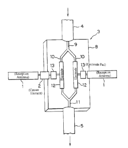
As illustrated in Fig. 3, the electric field
sensor head 3 comprises a substrate 8, an incident
optical waveguide 9, two phase-shift optical waveguides
10, an outgoing optical waveguide 11, and modulation
electrodes 12. The incident optical waveguide 9 is
formed on the substrate 8 to be connected to the incident
optical fiber 4. The two phase-shift optical waveguide
10 is formed on the substrate 8 to be branched from the
incident optical waveguide 9 and have a variable
refractive index which varies in response to the electric
field intensity. The outgoing optical waveguide 11 is
formed on the substrate 8 to be connected at one end to
the outgoing optical fiber 5 and at the other end to the
junction of the two phase-shift optical waveguides 10.
The modulation electrodes 12 are formed in the vicinity
of the two phase-shift optical waveguides 10. The
resonator circuit 2 is connected between one of the
modulation elect~odes 12 and the reception antennas 1.
The reception antenna 1 and the resonator circuit 2 are
connected through electrode pads 13 to the modulation
electrodes 12.
The substrate 8 is made of a lithium niobate
single crystal plate which is cut out perpendicularly to
a c axis. By diffusion of titanium, the incident optical
waveguide 9, the phase-shift optical waveguides 10, and
2I49267
the outgoing optical waveguide 11 are formed on the
substrate 8. An incident light beam is incident rom the
incident optical fiber 4 and passes through the incident
optical waveguide 9 to be branched to the two phase-shift
optical waveguides 10. When the reception antenna 1
receives the input signal, electric voltages are induced
and applied to the modulation electrodes 12 to produce,
in the two phase-shift optical waveguides 10, electric
field components having directions opposite to each other
in a depth direction.
As a consequence, variation in refractive index
is produced in the two phase-shift optical waveguides 10
due to an electrooptical effect so that a phase
difference is produced between light beams propagating
through the two phase-shift optical waveguides 10. The
phase difference has a level dependent upon the electric
field intensity applied to the modulation electrodes 12.
The light beams are joined and combined in the outgoing
optical waveguide 11 as an outgoing light beam having a
light intensity which varies due to an interference
therebetween. In other words, the outgoing light beam
emitted to the outgoing optical fiber 5 has an intensity
which varies in response to the electric field intensity
applied to the modulation electrodes 12. Such variation
in light intensity is measured by the optical detector 7
to thereby detect the electric field intensity applied to
the modulation electrodes 12.
214g267
The modulation electrodes 12 have a thickness not
smaller than l~um and a low resistance so that a
resonator device formed by the electric field sensor head
3, the reception antenna 1, and the resonator circuit 2
has a Q value not smaller than a predetermined value (for
example, 10). Fig. 4 shows an equivalent circuit of the
resonator device. In the resonator device, the electric
field sensor head 3 has a synthetic resistance re, a
synthetic inductance Le, and a synthetic capacitance Ce.
The reception antenna 1 has a radiation resistance ra.
The input signal has a voltage V. The resonator circuit
2 comprises a coil having an inductance Lp. Instead, the
resonator circuit 2 may comprise either a condenser or a
combination of a condenser and an inductor.
In the electric field sensor according to the
embodiment of this invention, the resonator circuit 2 is
connected to one of the modulation electrodes 12 to form
the resonator device in order to amplify a voltage
applied to the modulation electrode 12. An improved
sensitivity is obtained by increasing a Q value (voltage
ratio) of the resonator device.
Generally, the Q value of the resonator device is
represented by:
Q = 1/(2~fCR),
where f, C, and R represent a frequency, a capacitance
component, and a resistance component, respectively.
In order to improve the sensitivity, the
modulation electrodes 12 have an increased thickness in
21~9267
the embodiment of this invention to reduce the synthetic
resistance of the electric field sensor head 3. The
relationship between the thickness of the modulation
electrodes 12 and the synthetic resistance of the
electric field sensor head 3 is depicted by a curve A
illustrated in Fig. 5. In the embodiment of this
invention, the modulation electrodes 12 have a thickhess
not smaller than l~um.
Next, description will proceed to anothe~
embodiment of this invention with reference to Fig. 6.
In this embodiment illustrated in Fig. 6, the
modulation electrodes 12 comprise a plurality of split
electrodes 12a and 12b split in a light propagating
direction and capacitively coupled, respectively. The
reception antenna 1 for receiving an electric field is
implemented by a low radiation resistance antenna. In
this embodiment, the electric field sensor head 3 has a
small synthetic capacitance and the reception antenna 1
has a low radiation resistance. Thus, the Q value of the
resonator circuit is increased to thereby improve a
sensitivity of the electric field sensor.
As illustrated in Fig. 6, one of the two
modulation electrodes 12 comprises the split electrodes
12a, four in number. Likewise, the other of the two
modulation electrodes 12 camprises the split electrodes
12b, four in number. One of the split electrodes 12a
located at one end of an array of the split electrodes
12a is connected to the reception antenna 1. Likewise,
2149267
11
one of the split electrodes 12b located at the other end
of an array of the split electrodes 12b is connected to
the reception antènna 1 through the resonator circuit 2.
Except those cdnnected to the reception antenna 1, the
split electrodes 12a are connected to the split
electrodes 12b opposite thereto, respectively.
The reception antenna 1 comprises a 8JK beam
antenna which is one of the low radiation resistance
antennas and which is invented by John Claus. The 8JK
beam antenna has a basic structure illustrated in Fig. 7.
Dipole antenna elements la having a length L given by L =
~/2 (~ being the wavelength of a radio wave) are ar~anged
in parallel at an interval w as narrow as about ~/8.
Since the 8JK beam antenna is excited in reverse phase,
the radiation resistance is more and more reduced as the
interval w between the elements la becomes narrower.
The electric field sensor according to this
invention may comprise a waveguide or a reflector such as
a Yagi antenna. In this event, the sensitivity of the
electric field sensor is improved by concentration of the
radio wave.
Now, description will be made as regards a
specific example df this invention with reference to
numerical vaiues.
The substrate 8 was made of a lithium niobate
crystal plate (Z-cut plate). After the substrate 8 was
entirely coated with a silicon dioxide (SiO2) film as a
buffer layer for preventing light absorption, the
2149267
12
phase-shift optical waveguides 10 were formed on the
substrate 8 in the manner described above. A pair of the
modulation electrodes 12 were formed on the phase-shift
optical waveguides 10. In this case, the modulation
electrodes 12 we~e made of gold (Au). The electric field
sensor head 3 had a synthetic resistance not greater than
5 Q. The modulation electrodes have a thicknes5 of l~um.
Each of the modulation electrodes 12 was split into four
split electrodes in the light propagating direction so as
to make the electric sensor head 3 have a synthetic
capacitance of 3 pF (see Fig. 6).
The resistance and the capacitance of the
electric field sensor head 3 were measured by the use of
a network a~alyzer. As a result, the resistance was
equal to 5 Q (at a frequency of 500 MHz) and the
capacitance was equal to 3 pF. As the reception antenna
1, the 8JK beam antenna was prepared with the elements la
having an interval w defined by w = ~/10 and a length L
defined by L = ~/2 (see Fig. 7). The radiation
resistance of the 8JK beam antenna was measured by the
use of the network analyzer. As a result, the radiation
resistance was equal to 5 ~.
The resonator circuit 2 and the 8JK beam antenna
for reception were connected to the modulation electrodes
12 of the electric field sensor head 3 to test the
sensitivity in detection of the electric field. As a
result, it is found out that the sensitivity is improved
in correspondence to the Q value as compared with the
21~9267
conventionai electric field sensor. Specifically, the
optical detector 7 produced a detection signal of 75 dB/uV
when the radio wave of 500 MHz applied the electric field
intensity of 80 dB~uV/m.
For comparison, the conventional electric field
sensor (see Fig. 1) was prepared in the following manner
to test its sensitivity.
The conventional electric field sensor was made
of a similar material by a similar process as the
electric field sensor according to this inventian, except
that an electrode structure comprises a single electrode
having a thickness of 1000 angstroms and that the
reception antenna is implemented by a half-wave dipole
antenna.
The resistance and the capacitance of the
conventional electric field sensor head were measured by
the use of the network analyzer. As a result, the
resistance was equal to 50 Q (at a frequency of 500 MHz)
and the capacitance was equal to 12 pF. The radiation
resistance of the half-wave dipole antenna was equal to
73 Q.
Under a similar measurement condition, such as
the light source 6 and the optical detector 7, quite
similar to the above-mentioned embodiment, the
conventional electric field sensor was tested for the
sensitivity in detection of the electric field. As a
result, the optical detector 7 produced a detection
signal of 55 dBjuv when the radio wave of 500 MHz applied
2149267
14
the electric field intensity of 80 dBuV/m.
As described, the electric field sensor according
to this invention has a sensitivity higher by 20 dB than
that of the conventional electric field sensor. When the
electric field sensor according to the above-mentioned
embodiment was combined with the Yagi antenna with a
waveguide of 20 elements, the sensitivity was further
improved by 10 dB or more. When the film thickness of
the modulation electrode 12 was increased to twice or
more, the electric field sensor head 3 had a synthetic
resistance not greater than 4 Q and a synthetic
capacitance on the order of 1.5 pF. In this case, the
sensitivity was still further improved by 15 dB as
compared with the foregoing.
Next, still another embodiment of this invention
will be described.
Fig. 8 shows an electric field sensor of this
embodiment. The electric field sensor head is used in a
transmission system of a television relay broadcasting
network in which a transmission point and a reception
point are separated from each other. The transmission
system comprises those components similar to the
first-mentioned embodiment illustrated in Fig. 2 and
designated by like reference numerals. The transmission
system further comprises a photoelectric converter
circuit 14 for converting an outgoing light beam from the
outgoing optical fiber 5 into an electric signal, a
compensator circuit 15 for receiving the electric signal
21~9267
from the photoelectric converter circuit 14, and a
conversion amplifier circuit 16 for receiving the
electric signal from the compensator circuit 15. The
conversion amplifier circuit 16 is responsive to the
electric signal delivered from the photoelectric
converter circuit 14 through the compensator circuit 15
and converts the electric signal into an IF signal
(intermediate frequency signal) to be delivered to the
broadcasting network. Thus, an optical signal can be
directly modulated by a weak RF signal so that a receiver
section requires no battery.
Next, yet another embodiment of this invention
will be described.
Referring to Fig. 9, an electric field sensor
according to this embodiment is used in insulation of an
apparatus applied with a high frequency and a high
voltage.
For saving a cost, an STL reception parabolic
antenna lb is often attached to a medium-frequency aerial
17 having a length of about lOOm, as illustrated in Fig.
9. In this case, the medium-frequency aerial 17 is
applied with a high frequency and a high voltage. The
electric field sensor head 3 is grounded through a pole
gap 18. A medium-frequency transmitter 19 is connected
to a connection point between the electric field sensor
head 3 and the pole gap 18. By the use of the electric
field sensor according to this invention, a common
insulator is unnecessary as illustrated in Fig. 9. This
2149~67
16
makes it possible to reduce the cost.
Next, a further embodiment will be described.
Fig. 10 shows an electric field sensor which is
used in preventing a wire channel from being damaged by
thunderbolt. In this case, the electric field sensor
head 3 is connected to an external wire circuit 20
through an arrester 21 and a terminal resistor 22. By
the use of the electric field sensor according to this
invention, transmission and reception can electrically be
isolated so as to prevent destruction of a reception-side
apparatus due to thunderbolt or the like.
Although the description has thus far been made
in conjunction with the several embodiments, it will be
understood that this invention is not restricted thereto
and can be modified in various other manners. For
example, the electric field sensor head may be provided
with a reflector formed at the outgoing side of the
phase-shift optical waveguides. The incident light beam
passing through the phase-shift optical waveguides is
reflected by the reflector and returned back to the
incident side to be emitted therefrom. In this
structure, a single optical fiber is commonly used as
both the incident optical fiber and the outgoing optical
fiber.