Note: Descriptions are shown in the official language in which they were submitted.
CA 02149295 2000-11-30
SYNCHRONIZING BIGNAL DETECTION APPARATUS
The invention relates to an apparatus for detecting
a synchronizing signal for establishing synchronization in the
field of mobile communication, especially for reducing the
processing needed to detect the synchronizing signal using a
Digital Signal Processor.
Known apparatus for detecting a synchronization
signal comprises an antenna, a frequency converter for
converting from radio frequency (RF) to baseband (BB), a
filter, an A-D converter, a ~r/4 shift QPSK demodulator, an
error counter and a threshold discriminator. The apparatus
compares the input signal bit pattern with all of a known
synchronization signal bit pattern. Thus, where the length
of one frame of an input signal bit pattern is 1000 bits, and
the length of the known synchronizing signal bit pattern is
30 bits, a total of 30 x 1000, i.e. 30,000, comparisons must
be made.
There is another conventional apparatus which
processes the entire comparison in a special hardware for
detecting a synchronizing signal. In other words, the
conventional apparatus includes a synchronizing signal
detecting circuit for comparing always the input signal bit
pattern with 30 bits of the synchronizing signal bit pattern,
and for shifting the input signal bit pattern one after
another and for detecting a synchronizing signal when all 30
bit patterns are matched with the synchronizing signal.
Since the conventional synchronizing signal
detection apparatuses are constructed as described above, the
amount of processing increases in the conventional apparatuses
which compares all synchronizing signal bit patterns.
Therefore, a special hardware or a high speed signal processor
is required. Since these apparatuses consume a large amount
of electric power, they are inappropriate for the mobile
telephone.
According to one aspect of the present invention,
there is provided a synchronizing signal detection apparatus
comprising: a demodulator for digitally demodulating input
1
CA 02149295 2000-11-30
signals; a partial matching error counter for comparing every
bit of the demodulated input signal bit pattern demodulated
by the demodulator with a part of the known synchronizing
signal bit pattern; and a remaining bit matching counter for
comparing the input signal bit pattern with remaining bits of
the synchronizing signal bit pattern used in the partial
matching error counter, or with all synchronizing signal bit
pattern, for every bit, when an error bit number, which is
compared in the partial matching error counter, is equal to
or less than a first threshold value.
According to another aspect of the present
invention, there is provided a synchronizing signal detection
apparatus wherein the partial matching error counter compares
the input signal bit pattern with 10 to 25% of the
synchronizing signal bit pattern.
According to another aspect of the present
invention, there is provided a means for generating and
storing a corresponding complex synchronizing signal waveform
data from known synchronizing signal bit pattern; a partial
correlator for calculating correlation between sampled input
signal data and a part of the waveform data which is an output
data of the synchronizing signal waveform generation and store
means; and a remaining correlator for calculating complex
correlation between the input signal waveform data and
remaining synchronizing signal waveform data which is other
data stored in the synchronizing signal waveform generation
and store means, or all synchronizing signal waveform data,
when a correlation result calculated by the partial correlator
exceeds a first predetermined threshold value, and for
determining, when the correlation result calculated in the
remaining correlator is equal to or larger than a second
predetermined threshold value, that a synchronizing signal has
been detected.
According to another aspect of the present
invention, there is provided means for generating a
corresponding complex synchronizing signal waveform data from
known synchronizing signal bit patterns and for storing the
generated corresponding complex synchronizing signal waveform
2
CA 02149295 2000-11-30
data; a partial correlator for calculating correlation between
the sampled input signal data and a part of the waveform data
which is an output data of the synchronizing signal waveform
generation and store means; a time location store means for
storing a predetermined number of the time locations of an
input signal waveform data which corresponds to a large
correlation value calculated in the partial correlator; a
remaining correlator for calculating complex correlation
between the input signal waveform data which is stored in the
time location store means and remaining synchronizing signal
waveform data which is other data stored in the synchronizing
signal waveform generation and store means, or all
synchronizing signal waveform data; a demodulator for
demodulating a predetermined bit length of an input signal
waveform data which corresponds to a large correlation value
calculated in the remaining correlator; and a counter means
for comparing a bit pattern demodulated in the modulator with
the known synchronizing signal bit pattern for every bit, and
for determining, when the correlation result calculated in the
remaining correlator is less than a second predetermined
threshold value, that a synchronizing signal has been
detected.
In any of the foregoing aspects of the present
invention, the partial correlator may calculate complex
correlation between the input signal waveform data and 10 to
25% of the waveform generated by the synchronizing signal
waveform generation and store means.
By reducing the amount of processing, synchronizing
signal detection apparatus embodying the present invention may
detect a synchronizing signal easily using a digital signal
processor (DSP) having lower processing capability By reducing
the amount of processing.
In preferred embodiments of the invention, the
comparison bit numbers are from 10 to 250 of the synchronizing
signal, resulting in improved detection efficiency.
Embodiments of the present invention may provide
decreased detection time and amount of processing by
separating the correlation calculation of a part of the
3
' ' 2149295
synchronizing waveform data from that of a remaining
synchronizing waveform data, and without demodulating the bit
patterns.
Embodiments of the present invention may provide a
synchronizing signal detection apparatus for obtaining a small
error detection probability, by separating the correlation
calculation of a part of synchronizing waveform data from that
of a remaining synchronizing waveform data, and by calculating
bit patterns matching after demodulation is carried out.
Synchronizing signal detection apparatus according
to the present invention may improve detection efficiency by
using correlation bit numbers from 10 to 25% of the
synchronizing signal.
An embodiment of the invention will now be described
by way of example only with reference to the accompanying
drawings, in which:
FIG. 1 is a block diagram of a synchronizing signal
detection apparatus of a first embodiment of the present
invention.
FIG. 2 shows comparison number ratio between the
prior art and the first embodiment.
FIG. 3 is an operation flow chart of the apparatus
of the first embodiment of the present invention.
FIG. 4 is a block diagram of a synchronizing signal
detection apparatus of a second embodiment of the present
invention.
FIG. 5 is an operation flow chart of the apparatus
of the second embodiment of the present invention.
FIG. 6 is a block diagram of a synchronizing signal
detection apparatus of a third embodiment of the present
invention.
FIG. 7 is a first part of an operation flow chart
of the apparatus of the third embodiment of the present
invention.
FIG. 8 is a second part of an operation flow chart
of the apparatus of the third embodiment of the present
invention.
4
CA 02149295 2000-11-30
FIG. 9 is a block diagram of a conventional
synchronizing signal detection apparatus.
Construction of prior art apparatus for detecting
a synchronizing signal will first be described with reference
to FIG. 9, in which the numeral 1 denotes an antenna, the
numeral 2 denotes a frequency converter from RF (radio
frequency) band to BB (base band) , the numeral 3 denotes a
filter, the numeral 4 denotes an AD converter, the numeral 5
denotes a ~r/4 shift QPSK demodulator, the numeral 6 denotes
an error counter using all synchronizing signal bit patterns,
and the numeral 7 denotes a threshold discriminator.
Operation of the conventional synchronizing signal
detection apparatus shown in FIG. 9 is explained below. It
is assumed that the length of a signal bit pattern in one
frame is 1000 bits, wherein the length of the synchronizing
signal bit pattern is 30 bits, as an example. An input
analog signal inputted from an antenna is converted into a
digital signal in the analog/digital converter 4 and
demodulated into a digital demodulation bit pattern in the ~r/4
shift QPSK demodulator and is inputted to the error counter
6. The error counter 6 memorizes 30 bits of the synchronizing
signal bit pattern and compares all bits of the input signal
bit pattern and 30 bits of the synchronizing signal bit
patterns. Therefore, in the prior art, it is necessary to
compare the input signal bit pattern with all synchronizing
signal bit patterns for 30 x 1000 times, that is, 30,000
times.
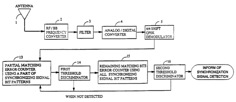
Embodiment 1
FIG. 1 is a block diagram of a synchronizing signal
detection apparatus of a first embodiment of the present
invention. In the first embodiment, the matching process
between the input signal bit patterns and the synchronizing
signal bit pattern is divided into two portions, one of which
is a partial matching process with a synchronizing signal bit
pattern and the other is a remaining matching process with the
remaining synchronizing signal bit pattern.
5
CA 02149295 2000-11-30
In FIG. 1, the numeral 13 denotes a partial matching
error counter for matching the input signal with the partial
synchronizing signal bit patterns, the numeral 14 denotes a
first threshold discriminator, the numeral 15 denotes a
remaining bits matching error counter 15 using all remaining
synchronizing signal bit patterns and the numeral 16 denotes
a second threshold discriminator. The frequency converter 2,
filter 3, analog-to-digital converter 4 and ~r/4 shift QPSK
demodulator 5 are the same as those in FIG. 9.
FIG. 3 is an operation flow chart of an apparatus
of the first embodiment of the present invention in FIG. 1.
In FIG. 3, "d" is an address of the input signal bit pattern
buffer, "sync" is an address of the synchronizing signal bit
pattern buffer, "p "' is a pointer which points the input
signal bit pattern buffer d. "1" is a synchronizing signal
bit pattern length used in the partial error counter 13, "N"
is a synchronizing signal bit pattern length, "L" is a buffer
length of the input signal bit pattern buffer d, "eor" is an
operator showing exclusive OR, "i" and "j" are count numbers
of loop counters, "Err" is a number of error bits, "THRESHOLD"
is a threshold of the error bit numbers which detects error
when Err is below this THRESHOLD value.
An operation of the first embodiment is explained
below. The radio frequency input signal received at the radio
antenna 1 is converted to a predetermined frequency band
signal by RF/BB frequency converter 2. The undesired signals
are filtered by the filter 3. The converted base band
frequency signal is converted to a digital signal by the
analog-to-digital converter 4, then demodulated into a
waveform of a digital bit pattern by ~r/4 shift QPSK
demodulator 5.
In step S1 of FIG. 3, the digital signal processor
(DSP) stores the demodulated digital bit patterns into a
predetermined buffer. The partial matching error counter 13
memorizes, for example, "1" bits which have a partial matching
with N bits synchronizing signals which serve as reference.
In step S3, the pointer p points to a top location
d of the input signal bit pattern buffer d, such as p = d.
6
CA 02149295 2000-11-30
First, in step S4, the error bit count Err and the loop count
i are initialized to zero. In step S5, every bit is counted
such as Err - Err + (p[i] eor sync [i]) until "1" bits is
compared. When all bits are compared in step S7, Err is
compared with THRESHOLD in step S8.
The first threshold discriminator 14 decides bit
numbers as to how many bits numbers are necessary to match
with for carrying out the comparing process in the remaining
bit matching error counter 15. For example, in step S8, the
error bit number Err is compared with THRESHOLD to determine
whether Err is above the threshold variable THRESHOLD. When
Err exceeds THRESHOLD in step S8 , the pointer p is incremented
in step S9 by one such as j = j + 1, which pointer p indicates
the input signal bit pattern buffer d address. In step S10,
j is compared with the length (L - N + 1). When j is within
the limit of (L - N + 1), the error count begins to count
again from the pointer p as defined in step S3 such as p = d
+ j. When j is not within the limit of (L - N + 1), the last
(N - 1) bit patterns from the address (d + L - N + 1) of the
input signal bit pattern buffer d are transferred to the range
of d - (d + N - 2) at step S11. A new input signal pattern
is inputted, and then the above error counting process is
restarted from the address d of the input signal bit pattern
buffer d.
In step S8, when Err is below THRESHOLD, the
remaining bits are compared again in the remaining bit
matching error counter 15. After initializing Err and loop
count i to zero in step S12, errors are counted at each bit
for all N bits in step S13 such as Err = Err + (p[i] eor sync
[i]) until i becomes N in step S15. When N bit comparison is
over, Err are compared with THRESHOLD in the second threshold
discriminator in step S16 to determine whether Err is larger
than the predetermined threshold variable THRESHOLD. When Err
is equal to or below the THRESHOLD for all N bits, it is
assumed that the synchronizing signal is detected. In step
517, the synchronizing signal detection address j on the input
signal bit pattern buffer d is then transferred to the time
control circuit, and then the error detection process is
7
CA 02149295 2001-O1-15
completed. Since the sampling time and the processing clock
of DSP are constant, respectively, the time when the
synchronizing signal exists is calculated by j.
FIG. 2 shows comparison number ratio between the
prior art and the first embodiment, in case the partial bit
pattern numbers of a known reference synchronizing signal bit
pattern are changed. For example, assume here that the
synchronizing signal bit pattern has 30 bits and the digital
demodulation bit pattern has 1000 bits in one frame. If the
input signal bit pattern is compared with 4 (= 1) bits of the
synchronizing signal bit pattern in the partial matching error
counter 13, and, if the input signal bit pattern is compared
with all 30 (= N) bits of the remaining bit matching error
counter 15, then the number of comparisons will be
1~ x 30 + (4 x 1000) = 5875 , which is approximately one fifth
2
of the 30,000 times of the prior art as shown in FIG. 2.
Embodiment 2
FIG. 4 is a block diagram of a synchronizing signal
detection apparatus of a second embodiment of the present
invention. In FIG. 4, the numeral 21 denotes a partial
correlator, the numeral 22 denotes a first threshold
discriminator, the numeral 23 denotes a remaining correlator,
the numeral 24 denotes a second threshold discriminator, the
numeral 33 denotes a circuit for generating and memorizing a
synchronizing signal waveform data from the synchronous signal
bit pattern.
FIG. 5 is a flow chart depicting operation of the
circuit 33 shown in FIG. 4. In FIG. 5, "r" is an address of
the input signal waveform data buffer, "sync" is an address
of the synchronizing signal bit pattern buffer, "sync "' is an
address of the synchronizing signal waveform data buffer r,
"8" is a ~r/4 shift QPSK transition angle which determines one
value for two synchronizing signal bits, "p"' is a pointer
which points the address of the receiving signal buffer, "1 "'
is a synchronizing signal waveform data length used in the
partial correlator 21, "N" shows a bit pattern length of all
synchronizing signal bit patterns, "N "' shows a data length
8
CA 02149295 2000-11-30
of all synchronizing signal waveform data, where N' - N / 2
+ 1. "L "' shows input signal waveform data buffer length
(buffer size of the input signal waveform data buffer r),
"conj" shows a complex conjugate, "abs" shows an absolute
value, "i", "j" show loop counters, "Cor" shows a correlation
value. "THRESHOLD "' is a threshold value of correlation
value, where it is deemed that the synchronizing signal is
detected when "Cor" is equal or above THRESHOLD'.
Operation of the apparatus of the second embodiment
will now be described with reference to FIG. 4 and FIG. 5.
An input signal received from the antenna is inputted into
partial correlator 21 by way of frequency converter 2, filter
3, and analog-to-digital converter 4 as a sampling waveform
data before digital demodulation is carried out.
The synchronizing signal generating and memorizing
circuit 33 generates and memorizes a synchronizing signal
waveform data which is a complex series defined by the known
synchronizing signal bit pattern and the modulation system.
Partial correlator 21 partially correlates the input
signal waveform data with a part of the synchronizing signal
waveform data which is generated and memorized in the
synchronizing signal generating and memorizing circuit 33.
In steps S21 to S25 in FIG. 5, a complex reference waveform
data of the synchronizing signal waveform data is generated
and memorized.
In step S26, DSP stores the necessary number of
input signal waveform data into the input signal waveform data
buffer r. In step S28 of FIG. 5, the partial correlator 21
points the correlation calculation starting pointer p' of the
input signal waveform data to the input signal waveform data
buffer r and correlates the input signal waveform data with
the complex synchronizing signal waveform data. The
correlator 21 functions to monitor the similarity of an input
signal waveform data and a complex synchronizing signal
waveform data. When the correlation of 1' waveform data is
taken, correlation calculation is completed when the
correlator 21 passes the loop for 1' times.
9
CA 02149295 2000-11-30
In step S33, the first threshold discriminator 22
judges the result of correlation calculation. When the
correlation is not larger than the predetermined threshold
value such as abs (Cor) < THRESHOLD', the pointer p' which
points to the correlation calculation starting address is
incremented by one such as j = j + 1, in step S34. Then, in
step S35, the value j is checked to determine whether j is
larger than (L' - N' + 1). In addition, the buffer length is
L' (r [ 0 ] ~ r [ L' - 1 ] ) and the correlation calculation is
completed until r [L' - (N - 1) - 1]. Therefore, the
correlation calculation is carried out after r [L' - N + 1].
In step S35, it is indicated such as j > L' - N' + 1 and a
sign is not used. It is because the increment step S34 of the
counter is located before the comparison step S35. When j is
equal to or smaller than (L' - N' + 1), the correlation
calculation is carried out again from the address defined in
step S28. If j is larger than (L' - N' + 1), the last (N' -
1) of waveform data in the input signal waveform data buffer
r is transferred to the address of the input signal waveform
data buffer r in step S36. That is, (N' - 1) data from the
address (r + L' - N' + 1) is transferred into the address
range of r ~ (r + N' - 2) of the input signal waveform data
buffer r. After a new input signal waveform data is inputted,
the correlation calculation mentioned above starts again from
the address of the input signal waveform data buffer r.
On the other hand, in step 533, when the correlation
is equal to or larger than the predetermined threshold value
such as abs (Cor) >_ THRESHOLD', the remaining correlator 23
initializes the correlation value (Cor) and the loop counter
i to zero, respectively, in step S37. Then, in step S38, the
correlation calculation is carried out for all N' waveform
data such as Cor = Cor + conj (p' [i] x sync' [i]), until i
reaches N' in step S40. When the correlation calculation is
completed, the second threshold discriminator 24 judges the
correlation result calculated in the remaining correlator 23
by determining whether abs (Cor) is smaller than THRESHOLD'.
When abs (Cor) is equal to or larger than the
THRESHOLD' for all N' bits, it is assumed that the
CA 02149295 2000-11-30
synchronizing signal is detected. In step 542, the
synchronizing signal detection address j on the input signal
waveform data buffer r is then transferred to the time control
circuit, and then the correlation detection process is
completed. Since the sampling time and the processing clock
of DSP are constant, respectively, the time when the
synchronizing signal exists is calculated by j.
According to the second embodiment, it is possible
to detect the synchronizing signal without demodulating the
digital bit pattern. That is, since it not necessary to
provide the digital demodulation process, less processing is
required than that in the first embodiment. With regard to
the bit number for the partial correlation, partial comparison
using the partial matching error counter of the first
embodiment in FIG. 2 can be applied to the second embodiment
in the same way.
Embodiment 3
FIG. 6 is a block diagram of a synchronizing signal
detection apparatus of a third embodiment of the present
invention. In FIG. 6, the number 29 denotes a partial
correlator which compares a sampled input signal waveform data
with a part of the reference waveform data of the complex
synchronizing signal stored, the number 30 denotes a time
location memory circuit which stores a predetermined number
of the input signal waveform data, the number 31 denotes a
remaining correlator, the number 32 denotes a maximum value
detector 32, the number 35 denotes a digital demodulator which
demodulates a receiving data having maximum value data for one
synchronous signal length, the number 36 denotes an error
counter 36 which uses all synchronous signal bits, and the
number 37 denotes a threshold discriminator. The frequency
converter 2, the filter 3, the analog-to-digital converter 4
and the mapping apparatus 33 are the same as those in the
above embodiments.
FIG. 7 and FIG. 8 are operation flow charts
depicting operation of the third embodiment of the present
invention shown in FIG. 6. In FIG. 7 and FIG. 8, "r" is an
11
CA 02149295 2000-11-30
address of an input signal waveform data buffer, "sync" is an
address of a synchronizing signal bit pattern buffer, "sync "'
is an address of a synchronizing waveform data buffer, "time"
is a data buffer for storing upper 10 time locations of the
correlation value, "Demod" is a digital demodulation bit
pattern buffer and "p"' is a pointer which points to the input
signal waveform data buffer r.
"Err" is the number of error bits, "Cor" is a
correlation value, "Cor "' is a temporary value of correlation
value, "MaxCor" is a maximum correlation value, "MaxCorTime"
is a time location of the maximum correlation value,
"THRESHOLD" is a threshold value of error bit number, "vect"
is a temporary value of delay detection, "1 "' is a syn-
chronizing signal waveform data length used in the correlator
29, "N" is a data length of all synchronizing signal bits,
"N"' is a data length of all synchronizing signal waveform
data buffer, "L "' is a data buffer length of input signal
waveform data buffer (buffer size of the input signal waveform
data buffer r), "conj" shows a complex conjugate, "abs" shows
absolute value, and "i", "j", and "n" are count numbers of
loop counters. "Real" shows a real part of the complex
number, "Imag" shows an imaginary part of the complex number,
and "eor" shows exclusive OR.
Operation of the third embodiment will now be
described with reference to FIG. 6 to FIG. 8. The
synchronizing signal generating and memorizing circuit 33
generates and memorizes a synchronizing signal waveform data
which is a complex series defined by the known synchronizing
signal bit pattern and the modulation system in the same way
as described in the second embodiment. The input signal is
also supplied to the partial correlator 29 in the same way as
described in the second embodiment. In step 553, DSP stores
this input signal waveform data (L' - N' + 1) into the
addresses from (r + N' - 1) of the input signal waveform data
buffer r.
The operations from steps S54 to S59 are similar to
those from steps S27 to S32 of the second embodiment in FIG.
5. The complex correlation of the input signal waveform data
12
CA 02149295 2000-11-30
r [j] ~ r [j + 1' - 1] with the synchronizing signal waveform
data sync' [0] ~ sync [1' - 1] are stored into Cor [j]. The
correlation calculation is continued until the correlation
calculation starting pointer p' indicates an address (r + L'
- N'). As described above with respect to the second
embodiment, the reference waveform data are complex series and
the correlation in the correlator 29 is obtained by
calculating discretely.
In step S62, when DSP completed the partial
correlation calculation for the predetermined input data
number, 10 correlation calculation starting addresses are
selected among the input signal waveform data which showed the
largest correlation. In step S63, the selected 10 correlation
calculation starting addresses are memorized into the time
location memory 30. In steps S64 to S69, the remaining
correlator 31 carries out the correlation calculation for
respective N' waveform data from 10 correlation calculation
starting addresses among the input signal waveform data, using
all reference complex synchronizing signal waveform data. In
step S70, abs(Cor') is compared with MaxCor, and if abs(Cor')
> MaxCor, the maximum value detector 32 selects a maximum
correlation value abs(Cor'), and stores its abs(Cor') into
MaxCor and time [n] into MaxCorTime, in step S71. Then, n is
incremented by one in step S72. The digital demodulator 35
demodulates the digital bit pattern which is located at the
maximum correlation location.
In the flow chart of FIG. 8, the ~r/4 shift QPSK
demodulator 35 demodulates the digital bit patterns, for
example, from step S74 to step S85. In step S86, the error
counter 36 initializes the loop count i and the error count
Err, then, in step S87, the error counter 36 calculates Err
value for all N bits of all synchronizing signal bit patterns
using the demodulated digital input signal bit pattern Demod
[i] such as Err = Err + (Demo [i] eor sync [i]).
In step S90, the threshold discriminator 37 judges
whether errors are less than a predetermined value THRESHOLD,
i.e. whether matching existed. If many matchings are found,
that is, if Err is less than THRESHOLD, the apparatus detects
13
CA 02149295 2000-11-30
a synchronizing signal in step S93. The detection of the
synchronizing signal, i.e. MaxCorTime, is informed to the time
control circuit and the synchronizing signal detection
operation is completed.
Compared with the second embodiment, no setting of
the threshold value is necessary in this third embodiment, so
the circuit realization becomes easier.
Those skilled in the art will recognize that many
modifications to the foregoing description can be made without
departing from the spirit of the invention. The foregoing
description is intended to be exemplary and in no way
limiting. The scope of the invention is defined in the
appended claims and equivalents thereto.
14