Note: Descriptions are shown in the official language in which they were submitted.
~1~9364
Diversity Reception Device
BACKGROUND OF THE INVENTION
(1) Field of the Invention
This invention relates to a diversity reception device
attached to a radio transmission equipment, specifically
relates to a diversity reception device that weights and
combines a plurality of reception signals.
(2) Description of the Prior Art
Currently, a digital transmission equipment is
transmitting the carrier signal modulated by the digital data
signal (basek~and signal) for effective data transmission. As
for modulating the carrier signal, several methods are adopted
such as: Amplitude Shift Keying (ASK) to vary amplitude of the
carrier signal according to the digital baseband signal
(modulation signal) Frequency Shift Keying (FSK) to displace
frequency of the carrier according to the modulation signal;
Phase Shift Keying ( PSK ) to vary phase of the carrier according
to the modulation signal; and Quadrature Amplitude Modulation
(QAM) to vary amplitude and phase of the carrier independently
according to the modulation signal.
It is well known that these digital modulation methods
applied to mobile radio communication are affected by fading,
a phenomenon caused by reflected or scattering electric wave,
which seriously deteriorate the quality of the received signal.
1
~~.49364
One of the effective methods for supplementing the reception
level deterioration is the diversity reception which receives
the signal in a plurality of lines.
Diversity reception is divided into the following types:
Selection Combiner ( SC ) for selecting a signal with the biggest
reception level among the signals received in the plurality of
lines before decoding; Equal-Gain Combiner (EGC) for combining
all the received signals with equal level before decoding; and
Maximal-Ratio Combiner (MRC) for weighting the received signals
in proportion to each reception level and combining the signals
before decoding.
Among the above three types, MRC most effectively
combines the signals because the bigger the reception level of
the signal is, or the less noise-affected the signal is, the
more weighted the signal is.
The current MRC is explained below.
FIG. ? shows the block diagram of a currently used
diversity reception equipment with MRC with four lines for
receiving signals. In the device, input terminals 101 to 104
receive the signals, phase shifters 105 to 108 arrange the
carriers' phases equally, then adder 109 combines the signals
and decoder 110 decodes the combined signal. In the above
process, adder 109 combines the signals in linear form because
each signal has been amplified in linear form.
FIG. 2 shows an Inphase Quadrature plane figure
representing how a current transmission equipment combines
2
~1493~~
signals. For convenience's sake, it shows the case of
combining two lines of signals.
Sl and S2 represent reception signals. S1S and S1N
respectively represent a signal element and a noise element of
S1. S2S and S2N respectively represent a signal element and
a noise element of S2.
Generally, the level of each noise element is equal
despite the size of received signal and the difference of
receiving lines (hereinafter branches). That is why the
reception si_nal in each branch is drawn as a point on the
circumference with the same radius from signal elements S1S and
S2S respectively (as (S1N~=~S2N~). In the diversity reception
device with MRC in FIG. 1, signals received from each branch
are combined in linear form, that is, S1 and S2 are combined
in vector, and the combined signal is input in the decoder.
However, since MRC requires a very high efficiency in
synchronizing the carrier phases when combining the signals,
a current reception device with MRC tends to use an expensive
Digital Signal Processor (DSP) to A/D convert the received
signal for digital processing. Also, for combining the signal
in linear firm, A/D converter with wide dynamic range is
required. In short, a reception device with MRC has problems
in its size and cost.
MRC also have the following defect. MRC may be a most
preferable combiner under such propagation condition as is
affected by only the random disturbance like thermal noise
3
~1~~3~~
because the received signals are just combined in linear form.
However, MRC is vulnerable to interference waves such as the
delay wave. Especially, when such waves are included in the
signal received in a branch with high reception level, the
signal is weighted much despite the bad quality, decreasing the
receiving performance heavily.
SUMMARY OF THE INVENTION
The first object of the present invention, in
consideration of the above mentioned problems, is to provide
a diversity reception device with MRC in simple configuration,
comprising oily small-scale digital circuits suitable for IC,
including a memory and an adder.
The above object is achieved by a diversity reception
device for weighting and combining a plurality of reception
signals. The diversity reception device comprises: a
plurality of phase demodulators for demodulating a phase of a
respective one of the plurality of reception signals and
outputting phase data consisting of a predetermined number of
bits: a convertor having a first input port which receives the
phase data, a second input port which receives a combination
coefficient consisting of a predetermined number of bits, a
first output port, a second output port, and a storage, for
outputting predetermined values stored in a place in the
storage specified by a combination of the phase data and the
combination coefficient, from the first output port and the
4
second output port upon input of the phase data and the
combination coefficient, the predetermined values concerning
respectively sine elements and cosine elements corresponding
to the plurality of reception signals; a sine elements adder
for adding up the predetermined values output from the first
output port; and a cosine element adder for adding up the
predetermined values output from the second output port.
The plurality of phase demodulators each may comprise:
a phase detector for detecting and outputting a phase of the
respective one of the plurality of reception signals a delay
for delaying, one symbol time, data output from the phase
detector; and a calculator for calculating a difference
between data output from the phase detector and data output
from the delay, and outputting a result as a phase difference
data.
In these diversity reception devices, a first storage
and a second storage output predetermined values if reception
signal and phase data output from phase demodulator are given.
Then, by adding up the predetermined values for each reception
signal, the received signals are combined to one. Therefore,
the present reception device dispenses with expensive
components such as DSP, and comprises only with small-scale
. digital circuits suitable for IC including a memory and an
adder.
The converter may comprise: a plurality of first
storage, corresponding to the plurality of reception signals
5
and storing calculation results obtained by a certain
calculation on all the combinations of sine of the phase data
multiplied by the combination coefficient, for fetching and
outputting, upon entering of the phase data and the combination
coefficient, one of the calculation results stored in a place
specified by a combination of the phase data as a first address
and the combination coefficient as a second address; and a
plurality of second storage, corresponding to the plurality of
reception sicrnals and storing calculation results obtained by
a certain calculation on all the combinations of cosine of the
phase data multiplied by the combination coefficient, for
fetching and outputting, upon entering of the phase data and
the combination coefficient, one of the calculation results
stored in a place specified by a combination of the phase data
as a first address and the combination coefficient as a second
address.
The convertor may comprise: a first storage storing
calculation results obtained by a certain calculation on all
the combinations of sine of the phase data multiplied by the
combination coefficient, for fetching and outputting, upon
entering of the phase data and the combination coefficient, one
of the calculation results stored in a place specified by a
. combination of the phase data as a first address and the
combination coefficient as a second address; a second storage
storing calculation results obtained by a certain calculation
on all the combinations of cosine of the phase data multiplied
6
~1~936~
by the combination coefficient, for fetching and outputting,
upon enteri.ig of the phase data and the combination
coefficient, one of the calculation results stored in a place
specified by a combination of the phase data as a first address
and the combination coefficient as a second address; a phase
selector containing a plurality of input ports connected to the
plurality of phase demodulator, and an output port connected
to the first storage and to the second storage, for selecting
a piece of phase data according to a certain instruction out
of the phase data input to the plurality of input ports, and
outputting the piece of phase data to the output port; a
combination coefficient selector containing a plurality of
input ports which receive a plurality of combination
coefficients, and an output port connected to the first storage
and to the second storage, for selecting a combination
coefficient according to a certain instruction out of the
plurality of combination coefficients input to the plurality
of input ports, and outputting the combination coefficient to
the output port; and a timing generator for providing
instructions to the phase selector and the combination
coefficient selector so that each of the plurality of reception
signals is selected sequentially by time division and that the
phase data and the combination coefficient of each of the
plurality of reception signals are sent synchronously to the
first storage and the second storage respectively.
The first storage may store calculated results of sine
7
X149364
of the phase data multiplied by the combination coefficient
raised to a power of 2, and the second storage stores
calculated results of cosine of the phase data multiplied by
the combination coefficient raised to the power of 2.
In the present diversity reception device, a plurality
of signals are combined by a first storage and a second storage
with a method of selecting the signals one by one. This
enables to minimize the size and the cost of the diversity
reception device.
The second object of the present invention is to provide
a diversity reception device that combines a plurality of
signals avoiding the influence of interference waves like delay
wave and outputs a high-quality signal.
The diversity reception device may further comprise:
a plurality of comparator, corresponding to the plurality of
reception signals and containing an input port and an output
port, for comparing a reception level input to the input port
consisting of a predetermined number of bits with a
predetermined value, and outputting a result from the
outputting port; a plurality of likelihood detector,
corresponding to the plurality of reception signals, for
detecting a distance between the phase data and a decision
point, and outputting the distance; and a plurality of
outputs, corresponding to the plurality of reception signals,
for outputting the reception level as the combination
coefficient if the result output from the plurality of
8
~3.493~4
comparators shows that the reception level is less than the
predetermined value, and outputting, as the combination
coefficient, a predetermined value based on the distance output
from the plurality of likelihood detectors multiplied by the
reception level if the result shows that the reception level
is not less than the predetermined value.
The diversity reception device may further comprise:
a plurality of comparator, corresponding to the plurality of
reception signals and containing an input port and an output
port, for comparing a reception level input to the input port
consisting of a predetermined number of bits with a
predetermined value, and outputting a result from the
outputting ports a plurality of likelihood detector,
corresponding to the plurality of reception signals, for
detecting a distance between the phase data and a decision
point, and outputting the distance; and a plurality of
outputs, corresponding to the plurality of reception signals,
for outputting the reception level as the combination
coefficient if the result output from the plurality of
comparators shows that the reception level is less than the
predetermined value, and outputting, as the combination
coefficient, a predetermined value based on the distance output
from the plurality of likelihood detectors multiplied by the
reception level if the result shows that the reception level
is not less than the predetermined value.
The first storage may store calculated results of sine
9
X149364
of the phase data multiplied by the combination coefficient,
and the second storage stores calculated results of cosine of
the phase data multiplied by the combination coefficient.
The diversity reception device may further comprise:
a plurality of combination coefficient calculators,
corresponding to the plurality of reception signals, for
detecting the distance between the phase data and the decision
point, and outputting, as the combination coefficient, a value
obtained by performing a certain calculation on the detected
distance.
The present diversity reception devices detect the
strength of the interference wave in each reception signal by
a likelihood detector, and, based on the strength, determine
how much each signal should be weighted. Unnecessary influence
of interference wave can be eliminated by setting such a
condition as the bigger the influence of the interference wave
in a received signal~is, the less weighted the signal is when
combined.
BRIEF DESCRIPTION OF THE DRAWINGS
These and other objects, advantages and features of the
invention will become apparent from the following description
thereof taken in conjunction with the accompanying drawings
which illustrate a specific embodiment of the invention. In
the drawings:
FIG.1 is a b~.ock diagram illustrating the configuration of a
214936~'~
current diversity reception device.
FIG.2 is an IQ plane figure expressing a signal combination in
a current diversity reception device.
FIG.3 is a block diagram illustrating the configuration of a
diversity reception device in the first embodiment of the
present invention.
FIG.4 is an IQ plane figure expressing a signal combination in
the diversity reception device in the first embodiment of the
present invention.
FIG.5 is a block diagram illustrating the configuration of a
diversity reception device in the second embodiment of the
present invention.
FIG.6 is a block diagram illustrating the configuration of a
branch of a diversity reception device in the third embodiment
of the present invention.
FIG.7 is a block diagram illustrating the configuration of a
diversity reception device in .the fourth embodiment of the
present invention.
FIG.B shows the eye-pattern of phase data output from phase
demodulators 329-332 of a diversity reception device in the
fourth embodiment of the present invention.
FIG.9 is an IQ plane figure expressing a signal combination in
the diversity reception device in the fourth embodiment of the
present invention.
FIG.10 is a block diagram illustrating the configuration of a
diversity reception device in the fifth embodiment of the
11
zm9~s4
present invention.
FIG.11 is a block diagram illustrating the configuration of
combination coefficient controllers 1004-1007 of the diversity
reception device in the fifth embodiment of the present
invention.
FIG.12 is a flowchart illustrating the operation of combination
coefficient controllers 1004-1007 of the diversity reception
device in the fifth embodiment of the present invention.
DESCRIPTION OF THE PREFERRED EMBODIMENTS
<First embodiment>
FIG.3 illustrates the configuration of a diversity
reception device with MRC in the first embodiment of the
present invention. The device comprises phase demodulators
329-332, I-element ROMs 317-320, Q-element ROMs 321-324, I-
element adder 325, Q-element adder 326, decision 327, and clock
regenerator 328.
Phase demodulators 329-332 comprise input terminals
301-304, phase detectors 305-308, phase delays 309-312, and
phase adders 313-316 respectively, each as a whole is a
differential detector of phase-detector type of Differential _.
Phase Shift Keying (DPSK) modulation method.
The r:~ception signals digitalized by A/D converter or
limiter, etc. enter through input terminals 301-304.
Phase detectors 305-308 output detected phases in
digital after comparing the phases of the signals input in
12
~1493~~
input terminals 301-304 with the phase of the local oscillator
that does not appear in the figures. That means, phase
detectors 305-308 do not require any linear amplifier because
only phase element, not the amplitude element, of the received
signal is necessary.
Phase delays 309-312 delay the detected phases output
from phase detectors 305-308 1 symbolic time and output the
delayed phases. 1 symbolic time indicates a time obtained
from the period of the received signal multiplied by the
exponent of 2 of the polyphase PSK (e. x., 2 for 4 phases (22),
and 3 for 8 phases (23)).
Phase adders 313-316 calculate the phase differences
between the detected phases and the delayed phases and output
the results as the phase data. The phase data provide phase
data ek corresponding to branch k.
I-eler~~ent adder 325 totals the values output from I-
element ROMs 317-320. Q-element adder 326 totals the values
output from Q-element ROMs 321-324.
Decision 327, synchronizing with the clock signal sent
from clock regenerator 328, synthesizes a vector from the
values from I-element adder 325 and Q-element adder 326,
decides whether the result value is bigger or less than the
preset threshold value, and outputs the decision result as
decoded data.
Clock regenerator 328 regenerates the clock signal
synchronizing with the data from I-element adder 325 and Q-
13
2149364
element adder 326, and sends the clock signal to decision 327.
The explanation is given below on how the present device
composing as above combines the signals.
FIG.4 is an IQ plane figure showing signals S1 and S2
input to the diversity reception device of FIG.1 and the
combined signal by the present invention. For convenience's
sake, only two received signals (S1 and S2) are selected for
this figure.
Phase demodulators 329 and 330 are differential
detectors of phase detection type. Therefore, signals S'1 and
S'2 output from the above phase demodulators contain only el
and 82 which are phase data of the received signals, and have
no amplitude data. Since the signals S' 1 and S' 2 have the same
size, on the IQ plane, they are represented as points on the
circumference whose center is the origin, as
S' lI=COS61
S' 1Q=sin91
s' 2I=cose2
S' 2Q=sine2.
These phase data 91 and e2 are sent to I-element ROMs
317 and 318 and Q-element ROMs 321 and 322.
I-element ROMs 317 and 318 receive phase data el and
82 and reception level RSSI, then weight RSSIz on the cosine
elements of S'1 and S'2 respectively; and output the result
values S"lI and S"2I, as
S"lI=RSSIZ ~ cosel
14
L
~~493~4
=RSSIZ~S' lI
S"2I=RSSIz ~ cose2
=RSSIZ~S' 2I.
Similarly, Q-element ROMs 321 and 324, upon receiving
phase data of and 62 and reception level RSSI, weight RSSI~ on
the sine elements of S'1 and S'2 respectively, and output the
result values S"1Q and S"2Q, as
S"1Q=RSSIz ~ sinel
=RSSIZ~S' 1Q
S"2Q=RSSIZ ~ sin82
=RSSIz ~ S' 2Q .
Then, I-element adder 325 obtains I-element of the
combined signal by adding S"lI and S"2I, represented as
I-element of combined signal = S"lI + S"2I.
Similarly, Q-element adder 326 obtains Q-element of the
combined signal by adding S"1Q and S"2Q, represented as
Q-element of combined signal = S"1Q + S"2Q.
With the above implementation, the combined signal by
MRC is obtained, and decision 327, the final step, decodes the
signal.
The explanation is given below on why RSSIz is used as
the weight coefficient when reception signals are combined.
Suppose the complex envelope of a signal received in k
th branch at t=nT is Zk(n), then MRC diversity output VMRC(n)
is represented as
VMRC(n) - EZk(n)~Zk*(n-1),
* indicates the complex conjugate. Zk(n-1) indicates
a signal one symbol before Zk(n).
Here, phase data VDDk of each branch is represented as
VDDk = Zk(n)~Zk*(n-1)/~Zk(n)~Zk*(n-1)~. Hence,
VMRC(n) - EVDDk~~Zk(n)~IZk*(n-1)~. Here,
(Zk(n)~=~Zk*(n-1)~. Therefore,
VMRC(n) - ~VDDk~IZk(n)~2.
Consequently, MRC diversity output VMRC(n) is obtained
with ~Zk(n)~2, replaceable with RSSI2, as the weight
coefficient on phase data VDDk.
As the above description clarifies, MRC diversity
reception device of the present invention can be composed with
such small digital circuits suitable for IC as memory, adder,
and shift register, dispensing with expensive DSP and the like.
Furthermore, this invention realizes the non-linear
amplification that takes a very simple composition on radio
circuit because a signal input to the present device need not
be linear. These elements bear a multiplier effect to decrease
the cost of the components of the current device, and decrease
the cost of the radio equipment as a whole.
<Second embodiment>
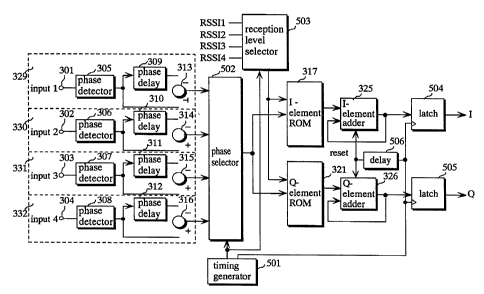
FIG.5 is a block diagram illustrating the configuration
of the MRC diversity reception device in the second embodiment
of the present invention. The present device differs from the
diversity reception device of the first embodiment in that
16
X149364
only two ROMs, I-element ROM 317 and Q-element ROM 321, are
provided to cover all the four branches. The same components
as those in the first embodiment have the same numbers in
FIG S .
The present device differs from the diversity reception
device of the first embodiment in that the present device
additionally has timing generator 501, phase selector 502,
reception level selector 503, latches 504 and 505, and delay
506.
Phase selector 502 sequentially selects phase data sent
from phase demodulators 329-332 synchronously with the clock
signal sent from timing generator 501, receives phase data from
the phase demodulator, and sends it to I-element ROM 317 and
Q-element ROM 321.
Similarly, reception level selector 503 sequentially
selects an input port out of a plural of input ports in 503
with the clock signal sent from timing generator 501, receives
the reception level of the signal input in the port, and sends
it to I-element ROM 317 and Q-element ROM 321. Phase selector
502 and reception level selector 503 select the same branch at
the same timing according to the clock signal.
I-element ROM 317 and Q-element ROM 321 output I-
. element and Q-element of each reception signal to I-element
adder 325 and Q-element adder 326 respectively. 325 and 326
accumulate each sent element four times, and the results are
stored in latches 504 and 505 respectively. Then, 325 and 326
17
219364
are reset by the clock signal sent from delay 506.
In this way, phase data and reception levels of four
branches of the same reception signal are sent to I-element ROM
317 and Q-element ROM 321 respectively by time division, and
the same comained signal as that of the first embodiment is
obtained at last.
As understood from the above process, while the device
of the first embodiment needs as many I-element ROMs and Q-
element ROMs as there are branches, the device of the present
embodiment has only one ROM for each element of the branch to
achieve the same performance. This enables an even smaller
and less-electricity device than the first embodiment.
<Third embodiment>
FIG.6 is a block diagram illustrating the configuration of a
branch of the MRC diversity reception device in the third
embodiment of the present invention.
The present device differs from the diversity reception
devices of the first and second embodiments in that the present
device additionally has timing generator 601, offset 602, adder
603, and selector 605, and that two ROMs are replaced by
storage 604.
Offset 602 and selector 605 operate synchronously
according to the clock signal sent from timing generator 601.
This enables the operational values corresponding to I-
element and Q-element stored in storage 604 to be fetched
18
X149364
alternately by time division and sent to I-element adder 325
and Q-element adder 326 respectively.
Offset 602 outputs two values of offset data according
to the clock signal sent from timing generator 601. If N bits
of data are input in adder 603, the data from 0 to (2"-1)
correspond to phases from 0° to 360°. Therefore, two values
with difference 2"-2 are output as offset data from offset 602
using the relation of cos9 - sin(9+90°).
For example, if N = 8, any of such combinations as 0 and
64, 64 and 128, 128 and 192 and the like is output from offset
602.
Adder 603 adds the above offset data to the phase data
of each branch, and sends the result value to an address in
storage 604.
In this way, the operational values corresponding to
I-element and Q-element stored in storage 604 are fetched
alternately by time~~division and are used to calculate I-
element and Q-element of the received signal.
As apparent from the above description, while the device
in the first and second embodiments require I-element ROM and
Q-element ROM, the device in the present embodiment has only
one ROM to replace the above components achieving the same
performance. This enables an even smaller and less-electricity
device than the first and second embodiments.
<Fourth embodiment>
19
~4~3~~
FIG.7 is a block diagram illustrating the configuration
of a diversity reception device in the fourth embodiment of the
present invention.
The present device differs from the diversity reception
device of the first embodiment in that the present device
additionally has combination coefficient calculators 701-704,
and that I-element ROMs 705-708 and Q-element ROMs 709-712
operate differently. The same components as those in the first
embodiment appear in FIG.7, having the same numbers, and are
not explained here.
Combination coefficient calculators 701-704 are ROMs
storing combination coefficient values which are obtained by
calculating all the possible distances between the decision
point and the phase data. When phase data is input from a
phase demodulator 329, 330, 331, or 332 as an address to a
respective combination coefficient calculator 701, 702, 703,
or 704, combination coefficient Ck that corresponds to a
distance between the decision point and the phase data is
output.
FIG.8 shows the eye-pattern of phase data at n/4 shift
QPSK. It shows demodulated phases of the phase data
synchronously taken. Distances Ll and L2 each indicate the
likelihood of the decision point of each phase against the
ideal decision point. The bigger the distance is, the more
ideal the signal is, that is, the lower the rate of
interference wave included in the reception signal is.
~~493~4
Combination coefficient calculators 701-704 output distances
L1 (>_0) and L2 (>_0) obtained by calculating the predetermined
function f(x), as
C1 = f(L1)
C2 = f(L2):
f(x) is determined based on the degree of the effect
of interference wave taken into account when the received
signal is combined. For example, when the received signal is
combined with the first-degree weight for the effect of
interference wave, it can be determined as
C1 = L1
C2 = L2.
I-element ROMs 705-708 store operational values of
Ck~cosek for all the combinations of combination coefficient
Ck and phase data 9k. When combination coefficient Ck and
phase data ek as addresses are input from combination
coefficient calculators 701-704 and phase adders 313-316
respectively, I-element ROMs 705-708 output a calculation
result of Ck~cosek corresponding to the combination.
Similarly, Q-element ROMs 709-712 store operational
values of Ck~sinek for all the combinations of combination
coefficient Ck and phase data 8k. When combination coefficient
Ck and phase data ek as addresses are input from combination
coefficient calculators 701-704 and phase adders 313-316
respectively. I-element ROMs 709-712 output calculation result
of Ck~sin9k corresponding to the combination.
21
214934
The way the present device combines the signals is
explained below.
FIG.9 is an IQ plane figure showing received signals
and a combined signal obtained by the present device. For
convenience's sake, only two received signals are shown in this
figure.
Phase demodulators 329 and 330 are differential detector
of phase detection type. Therefore, signals S1 and S2 output
from the above phase-demodulators contain only 81 and 82 which
are phase data of the received signals, and have no amplitude
data. Since the signals S1 and S2 have the same size, on the
IQ plane, they are represented as points on the same
circumference whose center is the origin. These phase data
el and e2 are sent to combination coefficient calculators 701
and 702, I-element ROMs 705 and 706, and Q-element ROMs 709 and
710.
Combination tcoefficient calculators 701 and 702
calculate combination coefficients C1 and C2 which are weights
used in combining received signals, and send the results to I-
element ROMs 705 and 706, and Q-element ROMs 709 and 710.
I-element ROMs 705 and 706, upon receiving phase data
81 and 82 and combination coefficients C1 and C2, weight
combination coefficients C1 and C2 on the cosine elements of
phase data 81 and o2, and output the result values S' lI and
S'2I, as
S' l I=C1 ~ cosel
22
~i49~s4
S'2I=C2~cose2.
Q-element ROMs 709 and 710, upon receiving phase data
el and 62 and combination coefficients C1 and C2, weight
combination coefficients C1 and C2 on the sine elements of
phase data 81 and 82, and output the result values S'1Q and
S'2Q, as
S'1Q=C1~sinel
S'2Q=C2~sin82.
Then, I-element adder 325 obtains I-element of the
combined sigi:al by adding S'lI and S'2I, as
I-element of combined signal = S'lI + S'2I.
Similarly, Q-element adder 326 obtains Q-element of the
combined signal by adding S'1Q and S'2Q, as
Q-element of combined signal = S'1Q + S'2Q.
With the above implementation, I-element and Q-element
of the combined signal is obtained, and decision 327, final
step, decodes the signal data.
As the above description clarifies, MRC diversity
reception device of the present invention can compose such
small digital circuits suitable for IC as memory, adder, and
shift register, dispensing with expensive DSP and the like.
Furthermore, the device of the present embodiment
differs from MRC device in that it obtains a combined signal
by weighting it with a coefficient based on the distance of the
phase data not by weighting the reception signal level. In
this way, the present device can remove the effect of
23
~~~93~4
interference wave because it less weights a reception signal
when bigger interference wave is included in the reception
signal.
<Fifth embodiment>
FIG.10 is a block diagram illustrating the configuration
of a diversity reception device in the fifth embodiment of the
present invention.
The present device differs from the diversity reception
device of the first embodiment in that the present device
additionally has likelihood detectors 1001-1003 and combination
coefficient controllers 1004-1007. The same components as
those in the first embodiment appear in FIG.10, having the same
numbers, and are not explained here.
Likelihood detectors 1001-1003 detect the distance
between the decision point and phase data output from phase
demodulators 329-332, and send the results to combination
coefficient controllers 1004-1007.
Combination coefficient calculators 1004-1007 compose,
as shown in FiG.ll, comparator 1101, multiplication coefficient
ROM 1103, and converter 1102.
Comparator 1101 have in itself an input port and an
output port, compare reception level consisting of the
predetermined number of bits input to the input port with the
predetermined value stored inside; and output the result from
the output port.
24
2149364
Multiplication coefficient ROM 1103 stores predetermined
value of multiplication Ak ~ Rk which covers all the combinations
of multiplication coefficient Ak, which is determined by
distance Lk, and reception level Rk. Multiplication
coefficient ROM 1103 selects a calculation result of Ak~Rk if
distance Lk and reception level Rk are input as addresses, and
send the sehcted value to converter 1102.
Converter 1102, according to the output result of the
comparator 1101, selects reception level Rk or Ak~Rk output
from multiplication coefficient ROM 1103, and output the result
as combination coefficient Ck.
Given below is the explanation of the operation in
obtaining the combined signal in the present device, mainly the
operation of combination coefficient controller 1004-1007 shown
in FIG.10.
FIG.12 is a flowchart illustrating the operation of
combination coefficient controllers 1004-1007.
_ Firstly, reception level Rk and distance Lk are input
to combination coefficient controller 1004-1007 (step 51201),
then comparator 1101 compares reception level Rk and the
predetermined value (step 51202).
If reception level Rk is smaller than the predetermined
value, converter 1102 selects contact A and outputs reception
level Rk as combination coefficient Ck ( steps 51203 and 51205 ) .
If reception level Rk is small, it means that the S/N ratio is
bad. In that case, even if distance Lk is short, it cannot be
z1493fi4
said that it is due to the effect of interference wave.
Therefore, when reception level Rk is small, the combination
signal is obtained by weighting only reception level Rk without
considering distance Lk. That means a branch with small
reception level Rk is treated the same as that in MRC diversity
device.
On the other hand, if reception level Rk is bigger than
the predetermined value, converter 1102 selects contact B and
outputs Ak~Rk, output from multiplication coefficient ROM 1103,
as combination coefficient Ck (steps S1204 and S1205).
Multiplication coefficient Ak is obtained by calculating
the predetermined function f'(x) with distance Lk, as
Ak = f'(Lk).
Here, f'(x) operates under the following conditions:
multiplication coefficient Ak = 1 if distance Lk is bigger than
the predetermined value; and
0 <_ Ak < 1 if distance Lk is smaller than the predetermined
value.
Accordingly, multiplication coefficient Ak - 1 and
combination coefficient Ck = reception level Rk if Rk is big
and S/N ratio is good and distance Lk is big and there is no
interference wave. That means a branch without interference
wave is treated the same as that in MRC diversity device.
On the other hand, Ak takes a small value if reception
level Rk is big and S/N ratio is good and Lk is small and there
is strong interference wave. That means a branch with strong
26
X149364
interference wave has a small combination coefficient, and the
effect of interference wave is decreased.
It goes without saying that the present device works as
MRC diversity device if the comparator uses predetermined
comparison value Rk at its maximum, and that it works as a
diversity device which weights multiplication coefficient if
the comparator uses Rk at its minimum.
As apparent from the above description, the present
device can compose small digital circuits suitable for IC as
memory, adder, and shift register, dispensing with expensive
DSP and the like. And the cost down of the whole radio
equipment is possible with the present device.
Furthermore, the device of the present embodiment
differs from MRC device in that it obtains a combined signal
by weighting it with a coefficient based on the distance of the
phase data not by weighting the reception signal level. In
this way, the present device can remove the effect of
interference wave because it less weights a reception signal
when bigger interference wave is included in the reception
signal. Accordingly, the present signal combination method
provides better combination signal than the current MRC.
The above embodiments are provided to help understand
the diversity reception device by the present invention. It
is apparent, however, that the embodiment of the present
invention is not limited to the above embodiments. The
27
X149364
following are examples of the possible applications:
(1) All the five embodiments above have four branches.
However, the number of branches is not limited to four. For
example, two or eight branches can be used with almost the same
composition in the present diversity reception device.
(2) ROMs used for combination coefficient calculators ?01-
704 in the fourth embodiment can be united to I-elements 705-
708, and Q-elements 709-712, that is, for example, in such
manner as most significant bit addresses of I-element ROMs 705-
708 and Q-element ROMs 709-712 have the distances between the
decision point and the phase data and the least significant bit
addresses of these ROMs have the phase data, and the
calculation results can be fetched from the addresses.
Although the present invention has been fully described
by way of examples with reference to the accompanying drawings,
it is to be noted that various changes and modifications will
be apparent to those skilled in the art. Therefore, unless
such changes and modification s depart from the scope of the
present invention, they should be construed as being included
therein.
28