Note: Descriptions are shown in the official language in which they were submitted.
- 2149~09
PULSE WIDTH MODULATION
FOR SPATIAL LIGHT MODULATOR WITH SPLIT RESET ADDRESSINa
TECHNICAL FIELD OF THE INVENTION
This invention relates to spatial light modulators
used for image display systems, and more particularly to
loading spatial light modulators with image data.
- 2149809
BACKGROUND OF THE INVENTION
Video display systems based on spatial light
modulators (SLMs) are increasingly being used as an
alternative to display systems using cathode ray tubes
(CRTs). SLM systems provide high resolution displays
without the bulk and power consumption of CRT systems.
Digital micro-mirror devices (DMDs) are a type of SLM,
and ~ay be used for either direct-view or projection
display applications. A DMD has an array of micro-
mechanical pixel elements, each having a tiny mirror thatis individually addressable by an electronic signal.
Depending on the state of its addressing signal, each
mirror element tilts so that it either does or does not
reflect light to the image plane. Other SLMs operate on
similar principles, with an array of pixel elements that
may emit or reflect light simu~taneously with other pixel
elements, such that a complete image is generated by
addressing pixel elements rather than by scanning a screen.
Another example of an SLM is a liquid crystal display (LCD)
having individually driven pixel elements. Typically,
displaying each frame of pixel data is accomplished by
loading memory cells so that pixel elements can be
simultaneously addressed.
To achieve intermediate levels of illumination,
between white (on) and black (off), pulse-width modulation
(PWM) techniques are used. The basic PWM scheme involves
first determining the rate at which images are to be
presented to the viewer. This establishes a frame rate and
a corresponding frame period. For example, in a standard
television system, images are transmitted at 30 frames per
second, and each frame lasts for approximately 33.3
milliseconds. Then, the intensity resolution for each
pixel element is established. In a simple example, and
assuming n bits of resolution, the frame time is divided
into 2n-1 equal time slices. For a 33.3 millisecond frame
2149809
period and n-bit intensity values, the time slice is
33.3/2n-1 milliseconds.
Having established these times, for each pixel of each
frame, pixel intensities are quantized, such that blacX is
0 time slices, the intensity level represented by the LSB
is 1 time slice, and maximum brightness is 2n-1 time slices.
Each pixel's quantized intensity determines its on-time
during a frame period. Thus, during a frame period, each
pixel with a quantized value of more than 0 is on for the
number of time slices that correspond to its intensity.
The viewer's eye integrates the pixel brightness so that
the image appears the same as if it were generated with
analog levels of light.
For addressing SLMs, PW~I calls for the data to be
formatted into "bit-planes", each bit-plane corresponding
to a bit weight of the intensity value. Thus, if intensity
is represented by an n-bit value, each frame of data has n
bit-planes. Each bit-plane has a 0 or 1 value for each
pixel element. In the simple P~M example described in the
preceding paragraphs, during a frame, each bit-plane is
separately loaded and the pixel elements addressed
according to their associated bit-plane values. For
example, the bit-plane representing the LSBs of each pixel
is displayed for 1 time slice, whereas the bit-plane
representing the MSBs is displayed for 2n/2 time slices.
Because a time slice is only 33.3/Z55 milliseconds, the SLM
must be capable of loading the LSB bit-plane within that
time. The time for loading the LSB bit-plane is the "peak
data rate".
A high peak data rate puts high throughput demands on
the design of SLMs. To minimize the peak data rate,
modifications to the above-described loading scheme have
been devised. These loading schemes are acceptable only to
the extent that they minimize visual artifacts in the
3S displayed image.
-
2149~0~
One such modification uses a specially configured SLM,
whose pixel elements are grouped into reset groups that are
separately loaded and addressed. This reduces the amount
of data to be loaded during any one time, and permits the
LSB data for each reset group to be displayed at a
different time during the frame period. This configurat~n
is described in U.S. Patent Serial No. (Atty Dkt No.
TI-17333), assigned to Texas Instruments Incorporated.
~9809
SUMMARY OF THE INVENTION
One aspect of the invention is a method of pulse-width
modulating frames of data used by a spatial light modulator
having individually addressable pixel elements. The
display period for each frame of data is divided into a
number of time slices. Each frame of data is format~ed
into bit-planes, with each bit-plane having one bit of data
for each pixel element and representing a bit-weight of the
intensity value to be displayed by that pixel element.
Each bit-plane has a display time corresponding to a number
of time slices. The bit-planes are then sub-formatted into
reset groups, each reset group having data for a group of
pixel elements to be addressed at a different time from
other pixel elements. The display times of reset groups
from bit-planes of one or more of the more significant bit
weights are segmented into two or more segments, which
permits those display times to be distributed throughout
the frame period. The loading of memory cells associated
with the pixel elements is then performed in three phases.
First, front-frame loading loads about half of the
seqments, such that, for all reset groups, seqments having
the same bit weight are loaded at substantially the same
time. Then, mid-frame loading loads the reset groups of
bit-planes of one or more of the less significant bits.
Finally, end-frame loading loads the remaining segments,
such that for all reset groups, segments having the same
bit-weight are loaded at substantially the same time.
A technical advantaqe of the invention is that
successfully implements data loading for split reset
configurations. It provides good picture quality, both
when the image is in motion and when it is still, by
combining features of different data loading methods. The
method does not require increased bandwidth or result in
lower light efficiency, as compared to other split reset
addressing methods.
21~3~9
BRIEF DESCRIPTION OF THE DRAWINGS
Figures 1 and 2 are block diagrams of imaqe display
systems, each having an SLM that is addressed with a split-
reset PWM data loading method in accordance with the
invention.
Figure 3 illustrates the SLM of Figures 1 and;2,
configured for split-reset addressing.
Figure 4 illustrates an example of a data loading
sequence in accordance with the invention.
Figure 5 further illustrates the loading of the less
significant bits of the se~uence of Figure 4.
Figure 6 illustrates another example of a data loading
sequence in accordance with the invention.
~1498~9
DETAILED DESCRIPTION OF THE INVENTION
Overview of SLM Dis~laY Svstems Usin~ PWM
A comprehensive description of a DMD-based digital
display system is set out in U.S. Patent No. 5,079,544,
entitled "Standard Independent Digitized Video System", and
in U.S. Patent Serial No. (Atty Dkt No. TI-17855),
entitled "Digital Television System", and in U.S. Patent
Serial No. _ (Atty Dkt No. TI- 17671), entitled "DMD
Display System". Each of these patents and patent
applications is assigned to Texas Instruments Incorporated,
and each is incorporated by reference herein. An overview
of such systems is discussed below in connection with
Figures 1 and 2.
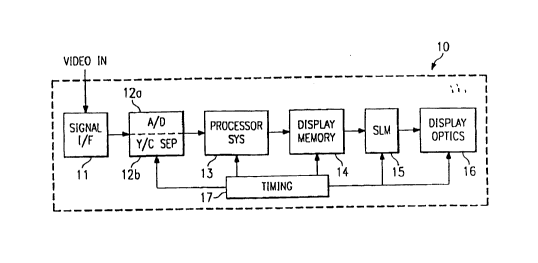
Figure 1 is a bloc~ diagram cf a projection display
system 10, which uses an SLM 15 to generate real-time
images from a analog video signal, such as a broadcast
television signal. Figure 2 is a block diagram of a
similar system 20, in which the input signal already
represents digital data. In both Figures 1 and 2, only
those components significant to main-screen pixel data
processing are shown. Other components, such as might be
used for processing synchronization and audio signals or
secondary screen features, such as closed captioning, are
not shown.
Signal interface unit 11 receives an analog video
signal and separates video, synchronization, and audio
signals. It delivers the video signal to A/D converter 12a
and YIC separator 12b, which convert the data into pixel-
data samples and which separate the luminance ("Y") data
from the chrominance ("C") data, respectively. In Figure
1, the signal is converted to digital data before Y/C
separation, but in other embodiments, Y/C separation could
be performed before A/D conversion, using analog filters.
-- 21~98o9
Processor system 13 prepares the data for display, by
performin~ various pixel data processing tasks. Processor
system 13 includes whatever processing memory is useful for
such tasks, such as field and line buffers. The tas~s
performed by processor system 13 may include linearization
(to compensate for gamma correction), colorspàce
conversion, and line generation. The order in which these
tasks are performed may vary.
Display memory 14 receives processed pixel data from
processor system 13. It formats the data, on input or on
output, into "bit-plane" format, and delivers the bit-
planes to SLM 16 one at a time. The bit-plane format
permits each pixel element of SLM 15 to be turned on or off
in response to the value of 1 bit of data at a time. In a
typical display system 10, display memory 14 is a "double
buffer" memory, which means that it has a capacity for at
least two display frames. The buffer for one display frame
can be read out to SLM 15 while the buffer another display
frame is being written. The two buffers are controlled in
a "ping-pong" manner so that data is continuously available
to SLM 15.
As discussed in the Bac~ground, the data from display
memory is delivered in bit-planes to SLM 15. Although this
description is in terms of a DMD-type of SLM 15, other
types of SLMs could be substituted into display system 10
and used for the invention described herein. For example,
SLM 15 could be an LCD-type SLM. Details of a suitable SLM
lS are set out in U.S. Patent No. 4,956,619, entitled
"Spatial Light Modulator", which is assi~ned to Texas
Instruments Incorporated, and incorporated by reference
herein. Essentially, DMD 15 uses the data from display
memory 14 to address its pixel elements. The "on" or "off"
state of each pixel element in the array of DMD 15 forms an
image.
214980g
U.S. Patent No. 5,278,652, entitled "DMD Architecture
and Timing for Use in a Pulse-Width Modulated Display
System", describes a method of formatting video data for
use with a DMD-based display system and a method of
addressing them for PWM displays. This patent application
is assigned to Texas Instruments Incorporated, and 'is
incorporated herein by reference. Some of the techniaues
discussed therein include clearing blocks of pixel
elements, usinq extra "off" times to load data, and of
breakinq up the time in which the more significant bits are
displayed into smaller segments. These techniques could be
used for any SLM using PWM.
Display optics unit 16 has optical components for
receiving the imaqe from SLM 15 and for illuminating an
image plane such as a display screen. For color displays,
the bit-planes for each color could be sequenced and
synchronized to a color wheel that is part of display
optics unit 16. Or, the data for different colors could be
concurrently displayed on three SLMs and combined by
display optics unit 16. Master timing unit 17 provides
various system control functions.
Split Reset Addressina
Figure 3 illustrates the pixel element array of SLM
lS, configured for split-reset addressing. Only a small
number of pixel elements 31 and their related memory cells
32 are explicitly shown, but as indicated, SLM 15 has
additional rows and columns of pixel elements 31 and memory
cells 32. A typical SLM 15 has hundreds or thousands of
such pixel elements 31.
In the example of Figure 3, sets of four pixel
elements 31 share a memory cell 32. As explained below,
this divides SLM 15 into four reset groups of pixel
elements 31. The data for these reset groups is formatted
into reset group data. Thus, where p is the number of
21~9~09
pixels and q is the number of reset groups, a bit-plane
having p number of bits is formatted into a rese~ group
having p/q bits of data. The reset groups are divided
"horizontally" in the sense that every fourth line of pixel
elements 31 belongs to a different reset group.
U.S. Patent Serial No. _ (Atty Dkt No. TI-17333~,
entitled "Pixel Control Circuitry for Spatial Light
Modulator", assigned to Texas Instruments Incorporated and
incorporated by reference herein, describes split-reset
data loading and addressing for a DMD. These concepts are
applicable to SLMs in general.
Figure 3 illustrates how a single memory cell 32
serves multiple pixel elements 31. Pixel elements 31 are
operated in a bistable mode. The switching of their states
from on to off is controlled by loading their memory cells
32 with a bit of data and applying a voltage indicated by
that bit to address electrodes connected to the pixel
elements via address lines 33. Then, the state of the
pixel element 31 is switched, in accordance with the
voltage applied to each, by means of a reset signal via
reset lines 34. In other words, for each set of four pixel
elements 31, either 1 or a O data value is delivered to
their memory cell 32, and applied to these pixel elements
31 as a "+" or "-" voltage. Signals on the reset lines 34
determine which pixel element 31 in that set will change
state.
One aspect of split-reset addressing is that only a
subset of the entire SLM array is loaded at one time. In
other words, instead of loading an entire bit-plane of data
at once, the loading for reset groups of that bit-plane's
data occurs at different times within the frame period. A
reset signal determines which pixel element 31 associated
with a memory cell 32 will be turned on or off.
The pixel elements 31 are grouped into sets of four
pixel elements 31, each from a different reset group. Each
2~9~09
set is in communication with a memory cell 32. In the
horizontal split reset example, pixel elements 31 from each
of the first four lines, each belonging to a different
reset group, share the same memory cell 32. The pixel
S elements 31 from each of the next four lines would also
share memory cells 32. The number of pixel elements~31
associated with a single memory cell 32 is referred to as
the "fanout" of that memory cell 32. The fanout could be
some other number. A greater fanout results in the use of
fewer memory cells 32 and a reduced amount of data loading
within each reset period, but reauires more resets per
frame.
In each set of four pixel elements 31, four reset
lines 34 control the times when the pixel elements 31
change state. Each pixel element 31 in this set is
connected to a different reset line 34. This permits each
pixel element 31 in a set to change its state at a
different time from that of the other pixel elements 31 in
that set. It also permits an entire reset group to be
controlled by a common signal on its reset lines 34.
Once all memory cells 32 for the pixel elements 31 of
a particular reset group have been loaded, the reset lines
34 provide a reset signal to cause the states of those
pixel elements 31 to change in accordance with the data in
their associated memory cells 32. In other words, the
pixel elements 31 retain their current state as the data
supplied to them changes, and until receiving a reset
signal.
PWM addressing se~uences for split-reset SLM's are
devised in accordance with various heuristic rules. One
rule is that the data for no more than one reset group can
be loaded at the same time. In other words, the loading of
different reset groups must not conflict. Other "optional"
rules are described in U.S. Patent Serial No. (Atty
2~49809
Dkt No. TI-17333), assigned to Texas Instruments
Incorporated and incorporated by reference herein.
one aspect of the invention is the recognition that
when split-reset loading is used for PWM, certain loading
se~uences cause visual artifacts, which can be avoided by
modifications to the loading sequence. Moreover, certàin
artifacts are related to the type of image being displayed.
A first type of artifact occurs during still images
and is seen as a contouring of particular levels in the
image as a function of rapid eye motion, motion of the SLM,
or interruptions such as caused by hand waving in front of
the face. This artifact is avoided by dividing the display
times of the bit-planes of the more significant bits into
smaller segments. For example, for a frame period having
255 time slices and 8-bit pixel values, the MSB, bit 7, is
represented by an on or off time of 128 time slices. The
MSB bit-plane data for each reset group is loaded at
different times but displayed for this 128 time-slice
duration. These 128 time slices can be divided into
segments. Typically, the segments are of equal duration,
but this is not necessary. The loading for the segments is
distributed throughout the frame period. This loading
method is referred to as an "interleaving method". The
bit-planes selected for segmentation could be any one or
more of the bit-planes other than that of the LSB.
A second type of artifact occurs during motion images,
where the viewer tracks the object undergoing motion. This
artifact is avoided by localizing as much illumination as
possible into an instantaneous burst. Subject to the rule
that no two reset groups can be loaded at once, data for
the same bit-weights of all reset groups are loaded near
together in time. This addressing method is referred to as
a "alignment method".
Figures 4 - 6 illustrate how aspects of both
interleavinq and aligning can be combined to result in a
- 21~98og
data loading sequence that minimizes visual artifacts for
both still and motion images. In each of the following
methods, 8-bit pixel values are assumed, so as to provide
256 levels of brightness resolution. Also, for purposes of
simplicity, only 4 reset groups are assumed. However, the
same concepts are applicable to pixel values with~ a
different resolution, as well as to SLMs having fewer or
more reset groups.
Tem~orallY Correlated MSB Addressinq
Figures 4 and 5 illustrate one example of a method of
loading data formatted for PWM on a split-reset SLM. This
method combines features of both interleaving and aligning.
Bit-plane segments (for bits 5 - 7) or unsegmented bit-
planes (for bits 0 - 4) are loaded in the basic sequence
illustrated in Figure 4. Each reset group is loaded in
this same sequence, with the exception being the
unsegmented bit-planes (bits o - 4), whose loading sequence
is illustrated in Figure 5. Figures 4 and 5 are intended
to illustrate loading sequences as opposed to display
timing -- an example of both loading sequence and display
timing is illustrated in Appendix A.
Consistent with the interleaving method, the more
significant bits (bits 5 - 7) are split into segments,
which are distributed throughout the frame period.
However, consistent with the alignment method, the
distribution of the more significant bit seqments is time-
ordered rather than random. The time-ordering calls for
loadi~g the more significant bits in a regular sequence
such that segments of the same bit weight are displayed at
nearly the same time for all reset groups. The bit-planes
for the less significant bits are loaded during the middle
of the frame period.
More specifically, the more significant bits, bits 7 -
S, are broken into segments. Bit 7 has 14 segments, bit
-
2149809
6 has 8, and bit 5 has 4. Each segment is 16 time slices
long, except for two segments of bit 7, one immediately
before and one immediately after the less significant bits.
As explained below, these two segments may be used as
"buffer segments" when there is a large number of reset
groups. If the number of reset groups is small, the buffer
segments may not be required and all segments of a bit-
plane could be a constant size. The less significant bits,
bits 4 - 0, are not broken into segments. Bit 4 has 16 LSB
periods, bit 3 has 8, bit 2 has 4, bit 1 has 2, and bit 0
has 1.
The loading of each frame of data has three phases --
front-frame loading, mid-frame loading, and end-frame
loading. During front-frame loading, the segments for bits
5 - 7 are loaded in a regular se~uence. 8y 'Iregular'' is
meant that each reset group is loaded in the same sequence.
During mid-frame loading, bits 0 - 4 are loaded. The
loadinq sequence of bits 0 - 4 varies among the reset
groups so as to avoid conflicts. During end-frame loading,
all segments of bits 5 - 7 remaining in the frame are
loaded in a regular pattern.
During loading, for each next reset group, the loading
of corresponding segments or unsegmented bit-planes is
staggered by at least one time slice. Although the result
is a slight "skew" from each reset-group to the next, the
staggering satisfies the rule that no two reset groups can
be loaded at the same time. Typically, it is desirable to
minimize the skew to only one time slice, but as explained
below, avoiding conflicts when loading less significant
bits may require a greater skew.
Figure 5 illustrates an example of the mid-frame
loading of the less significant bits, which varies among
reset groups. In the example of Figure 5, there are four
reset groups, designated as RG(1), RG(2), RG(3) and RG(4).
21~9~09
In general, the smaller the number of reset groups, the
simpler it is to avoid loading conflicts.
Figures 4 and 5 also illustrate the relationship
between the number of loads per frame and the number of
time slices per frame. The number of loads per frame
cannot exceed the number of time slices of a frame. The
number of loads per frame is the number of segments and
unsegmented bit-planes, times the number of reset groups.
In the example of Figures 4 and 5, for each reset group,
there are 14+8+4 (26) segments of bits 7 - 5 and 5 bit-
planes for bits 4 - 0. Thus, there are 26+5 = 31 loads per
frame per reset group. With 4 reset groups, the number of
loads per frame is 31*4 = 128. This is an acceptable
segmentation scheme because 128 is less than 2S5, the
number of time slices.
Appendix A illustrates how the loading sequence of
Figures 4 and 5 may be adapted for SLMs having a larger
number of reset groups. As the number of reset groups
increases, the number of time slices required to load data
per frame increases. For example, an SLM having 16 reset
groups and following the segmentation scheme of Figures 4
and 5, requires 31 * 16 = 496 loads per frame. This may be
accomplished by dividing the frame into 510 time slices
instead of 255. Each segment of bits 7 - 5 and each bit-
plane for bits 4 - 0 is displayed for twice as many time
slices. For example, the LSB bit-plane is displayed for
two time slices rather than one.
Also, as illustrated by Appendix A, as the number of
reset groups increases, the number of loads for the less
significant bits may increase past the time slices that
they are allocated. For example, an SLM that has 16 reset
groups and follows the sequence of Figure 4, requires 5 *
16 = 80 loads to load bits 4 - o. However, where there are
510 time slices per frame, the mid-frame loadin~ of bits 4
- o is alloc~ted a total of only 62 time slices. To
`_ 21498~9'
accommodate the increased number of mid-frame loads, the
staggering of the reset group load times is inCreased.
During mid-frame loading, the loading for the first bit-
plane is delayed by 3 time slices from one reset group to
S the next. As a result, the size of the "buffer segment"
immediately preceding this bit-plane "grows" by 3 t`ime
slices from one reset group to the next. To re-align the
reset groups after mid-frame loading, the "buffer segment"
immediately following the last mid-frame bit-plane
"shrinks" by 3 time slices for each next reset group.
Figure 6 illustrates another method of split-reset PWM
addressing. Like Figures 4 and 5, Figure 6 illustrates a
sequence that combines features of both interleaving and
aligning. However, in the method of Figure 6, bits 3 and
lS 4 as well as bits 7 - S, are segmented. Thus, bits 3 - 7
are treated as the more significant bits.
The segments of bits 3 - 7 are loaded in a regular
sequence such that segments of the same bit weight are
loaded at nearly the same time for all reset groups. The
bit-planes for bits 2 - 0 are loaded at the middle of the
frame period. The rule that no two reset groups can be
loaded at once is satisfied by staggering the loading at
least one time slice.
As in the method of Figures 4 and S, the segments
2S immediately before and after the mid-frame loading of the
less significant bits may be used as "buffer segments" when
the number of reset groups is too large to avoid conflicts
without them. However, for the same reason, the segments
immediately before and after the bit 3 se~ments may also be
used as "buffer segments". As explained above, this means
that the size of these segments may grow and shrink from
reset group to reset group, which permits loading of the
less significant bits to be staggered an extra amount.
The method of Figures 4 and S and the method of Figure
3s 6 have several common features. Bit-planes of the more
- _ 21~98og
significant bits are segmented. To the extent possible,
bit segments are temporally aligned. However, as ~he bit-
weight of the seqment decreases and the number of reset
groups increases, it becomes more difficult to align the
data and still avoid loadinq conflicts. Thus, the bit-
planes of less significant bits are concentrated in m~id-
frame and are "scrambled" rather than temporally aligned.
Also, "buffer seqments" are used to permit increased
staggering so that number of reset groups does not prohibit
some degree of alignment of the mid-frame bits or segments
of bit-planes of less significant bits.
Orderinq of Reset GrouDs
Another aspect of the invention is that the order in
which reset groups are addressed has an effect on whether
artifacts occur. For example, in a horizontal split reset
configuration, where n reset groups are arranged as every
nth line of a display, certain reset group patterns can
reduce the perception of strobing. In particular, a "by 3"
pattern is desirable.
For an SLM having 16 horizontal reset groups, such
that every 16th line is in the same reset group, an example
of a "by 3" orderinq pattern is as follows:
1 4 7 10 13 0 3 6 9 12 lS 2 5 8 11 14
2S In other words, all rows of the 1st reset group are loaded,
then all rows of the 4th reset group, in a series of every
third reset group. Then, beginninq with the 0th reset
group, every third reset group is loaded. Finally, a third
series of every third reset group, beginning with the 2d
reset group, is loaded. In general, the reset groups are
loaded in n series of every nth reset group, and the
sequence can be begin with any reset group.
2~ ~9~o~
18
Other Embodiments
Althou~h the invention has been described with
reference to specific embodiments, this description is not
meant to be construed in a limitinq sense. Various
modifications of the disclosed embodiments, as well as
alternative embodiments, will be apparent to persons
skilled in the art. It is, therefore, contemplated that
the appended claims will cover all modifications that fall
within the true scope of the invention.
- 2149~
APPENDI~ A
19
me Slice
rlumber Resel group numbcr:
1 2 3 4 S 6 7 8 9 10 11 12 13 14 lS 16
2 1 7
3 1 1 7
4 1 1 1 7
1 1 1 1 7
6 1 1 1 1 1 7
7 1 I' I I I 1 7
8 1 l I l l l I
9 1 1 1 1 1 1 1 1 7
1 1 1 1 1 1 1 1 1 7
11 1 1 1 1 1 1 1 1 1 1 7
12 1 1 1 1 1 1 1 1 1 1 1 7
13 1 1 1 1 1 1 1 1 1 1 1 1 7
14 1 1 1 1 1 1 1 1 1 1 1 1 1 7
1 1 1 1 1 1 1 1 1 1 1 1 1 1 7
16 7 1 1 1 1 1 1 1 1 1 1 1 1 1 1 7
17 6 7 1 1 1 1 1 i I l l l l l l I
18 1 6 7 1 1 1 1 1 1 1 1 1 1 1 I j
19 1 1 6 7 1 1 1 1 1 1 1 1 1 1 1 1
1 1 1 6 7 1 1 1 1 1 1 1 1
21 1 1 1 1 6 7
22 1 1 1 1 1 6 7 1 1 . I l l l l l I
23 1 1 1 1 1 1 6 7
24 1 1 1 1 1 1 1 6 7
1 1 1 1 1 1 1 1 6 7
26 1 1 1 1 1 1 1 1 1 6 7
27 1 1 1 1 1 1 1 1 1 1 6 7
28 1 1 1 1 1 1 1 1 1 1 1 6 7
2g 1 1 1 1 1 1 1 1 1 1 1 1 6 7
1 1 1 1 1 1 1 1 1 1 1 1 1 6 7
31 1 1 1 1 1 1 1 1 1 1 1 1 1 1 6 7
32 6 1 1 1 1 1 1 1 1 1 1 1 1 1 1 6
33 7 6 1 1 1 1 1 1 1 1 1 1 1 I j
34 1 7 6
1 1 7 6
36 1 1 1 7 6 1 1 1 1 1 1 1 1 1 1
37 1 1 1 1 7 6 1
38 1 1 1 1 1 7 6 ~ I l l l l l l I
39 1 1 1 1 1 1 7 6
g I I I I I I 1 7 6
41 1 1 1 1 1 1 11 7 6
42 1 1 1 1 1 1 11 1 7 6
~3 1 1 1 1 1 i II I 1 7 6
44 1 1 1 1 1 1 11 1 1 1 7 6 ~ I I
4S I I I I I I II I I I 1 7 6
46 ~ l l l I 1 7 6
47 1 1 1 1 1 1 11 1 1 1 1 1 1 7 6
48 7 1 1 1 1 1 iI I I I I I I 1 7
49 5 7
I S 7 ~ I i l l l l l l l l l I
51 1 1 5 7
52 1 1 1 5 7
53 I j I 1 5 7
54 ~ I I I I I 5 7
1 1 1 1 1 1 5 7
56 1 1 1 1 1 1 1 5 7
57 1 1 1 1 1 1 1 1 5 7
58 1 1 1 1 1 1 1 1 1 5 7
59 1 i I I I I I I I 1 5 7
1 1 1 1 1 1 1 1 1 1 1 5 7
21~9809
61 1 1 1 1 1 1 i I I I I I S 7
62 1 1 1 1 1 1 1 1 1 1 1 1 1 5 7
6~ 1 1 1 1 1 1 1 1 1 1 1 1 i I S 7
64 5 1 1 1 1 1 1 1 1 1 1 1 1 1 1 5
7 5
66 1 7 5 1 1 1 1 1 1 1 1 1 1 1 1 1
67 1 1 7 5 1 1 1 ~ I l l l l l l I
68 1 1 1 7 5
6g 1 1 1 1 7 5
1 1 1 ~ I 7 5 1 1 1 ~ I l l l I
71 1 1 1 1 1 1 7 5
72 1 1 1 1 1 1 1 7 5
73 1 1 1 1 1 1 1 1 7 5
74 1 1 1 1 1 1 1 1 1 7 5
1 1 1 1 1 1 1 1 1 1 7 5
76 1 1 1 1 1 1 1 1 1 1 1 7 5
77 1 1 1 1 1 1 1 1 1 1 1 1 7 5
78 1 1 1 1 1 1 1 1 I j I I 1 7 5
79 1 1 1 1 1 1 1 ~ I I I I I 1 7 5
ao 7 1 1 1 1 1 1 1 1 1 1 1 1 1 1 7
81 6 7
82 1 6 7
83 1 1 6 7
84 1 1 1 6 7
~5 1 1 1 1 6 7
86 1 1 1 1 1 6 7
87 1 1 1 1 1 1 6 7
88 1 1 1 1 1 1 1 6 7
89 1 1 1 1 1 1 1 1 6 7
go I I I I I I ~ I 1 6 7
91 1 1 1 1 1 1 1 1 1 1 6 7
92 1 1 1 1 1 1 1 1 1 1 1 6 7
93 1 1 1 1 1 1 1 1 1 1 1 1 6 7
94 1 1 1 1 1 1 1 1 1 1 1 1 1 6 7
1 1 1 1 1 1 1 1 ~ I I I I 1 6 7
96 6 1 1 1 1 1 1 1 1 1 1 1 1 1 1 6
97 7 6
98 1 7 6
99 1 1 7 6 1 1 1 ~ I l l l l l l I
lO0 1 1 1 7 6
101 1 1 1 1 7 6
102 1 1 1 1 1 7 6
103 1 1 1 1 1 1 7 6
104 1 1 1 1 1 1 1 7 6
105 1 1 1 1 1 1 1 1 7 6
106 1 1 1 1 1 1 1 1 1 7 6
107 1 1 1 1 1 1 1 1 1 1 7 6
108 1 1 1 1 1 1 1 1 1 1 1 7 6
109 1 1 1 1 ~ I I 1 7 6
110 1 1 1 1 1 1 1 1 1 1 1 1 1 7 6
111 1 1 1 1 1 1 1 1 1 1 1 1 1 1 7 6
112 7 1 1 1 1 1 1 ~ I I I I I I 1 7
113 6 7 1 1 1 1 1 1 ~ I l l l l l I
114 1 6 7 1 1 1 1 ~ I l l l l l l I
115 1 1 6 7
116 1 1 1 6 7
117 1 1 1 1 6 7
118 1 1 1 1 1 6 7
119 1 1 1 1 1 1 6 7 I r l l l l l I
120 1 1 1 1 1 1 1 6 7
121 1 1 1 1 1 1 1 1 6 7
122 1 1 1 1 1 1 1 1 1 6 7
123 1 1 1 1 1 1 1 1 l 1 6 7
12~ 1 1 1 1 1 1 1 1 1 1 1 6 7
125 1 1 1 1 1 1 1 1 1 1 1 1 6 7
126 1 i I I I I I I I I I I 1 6 7
127 1 1 1 1 1 1 1 1 1 1 1 1 1 1 6 7
~ W ~ ~ o ~ ~ _) ~ (n ~ ~ ~ 1--o ~ P W ~ ~--o ~ W ~ ~ O ~ 0~ , n Ul "~ w ~ I~ o ~ co ~ n ~ W ~ 1' o ~ co ~~ n ~ W ~ ~--o ~
--I a~-------- ------ --_ _ _ __ _ O~ ~1 _ _ _ _ _ _ _ _ _ __ _ __ ~ ~1_ _ __ __---------------- u- ~----. ---------------------- --~ a~--
a~--------------------------_ O~ ~1--------___--------___ ~1~______----------------I.n -~----------------------------~ a~----
o
~I
21 ~9~0~
195 1 1 7 6
196 1 1 1 7 6 1 I t l l l l l l l I
197 1 i I 1 7 6
198 1 1 1 1 1 7 6
199 1 1 1 1 1 1 7 6
200 1 1 1 1 1 i 1 7 6
201 1 1 ~ I I I I 1 7 6
202 1 1 1 1 1 1 1 1 1 7 6
203 i I I I I I I I I 1 7 6
204 1 1 1 1 I j I ~ I I 1 7 6
205 1 1 1 1 1 1 1 ~ I I I 1 7 6
206 1 1 1 1 1 1 1 ~ ~ I I I 1 7 6
207 1 ~ I I I I I I I I I I I 1 7 6
208 1 1 1 1 1 1 1 1 1 1 1 1 1 7
209 7 i I l l l l l I
210
211
212 1 7 1 1 1 1 1 . I l l l ~ l l l I
213
214 3
215 1 1 7
216 1 1 3
217 1 3
218 1 1 1 7
219
220 ~ I l l l ~ l l l l l l l I
221 1 1 1 1 7
222
223 1 1 1 3
224 1 1 1 1 1 7 1 1 1 1 ~ I l l l I
225
226 1 1 1 1 4 1 1 1 1 ~ I l l l l I
227 1 1 1 1 1 1 7
228 1 1 1 1 1 1 2
229 3 1 1 1 1 3
230 4 1 1 1 1 1 1 7
231 1 1 3 1 1 1 1 3
232 1 3 4 1 1 ~ I ~ l l l l l l l I
233 1 0 1 1 1 1 1 1 7
234 1 0 1 1 1 1 1 1 2
235 1 4 1 1 1 1 2
236 ~ I I I I I 0 1 1 7
237 1 1 1 1 1 1 0
238 1 1 1 3 1 1 3
239 1 1 1 4 1 1 1 1 1 1 7
240 1 1 1 1 1 1 1 1 1 1 3
2gl 1 1 1 1 1 1 1 1 2 3
242 1 1 1 1 1 1 1 1 0 1 1 7
243 1 1 1 1 1 1 1 1 0 1 1 3
244 1 1 1 1 1 3 ~ I 1 1 1 1 1 1 1 1
245 1 1 1 1 ~ 4 1 1 1 1 1 1 7
246 1 1 1 1 1 1 1 3
247
248 1 1 1 1 1 1 1 1 4 1 1 1 1 7
249 1 1 1 1 1 1 1 1 1 1 1 1 1 3
250 1 1 1 1 1 1 1 1 1 1 1 1 4
251 1 1 1 1 1 1 1 0 1 1 1 1 1 1 7
252 1 1 1 1 1 1 1 0 1 1 1 1 1 1 3
253 1 1 1 1 1 1 3 2
254 1 1 1 1 1 1 4 1 1 1 1 1 1 1 1 7
255 1 1 1 1 1 1 1 1 1 1 3 1 1 1 1 2
256 1 1 1 1 1 1 1 1 1 3 4
257 1 1 1 1 4 1 1 1 I g l l l l l I
258 1 1 1 1 0 1 1 1 1 1 1 3
259 1 ~ I I 0 1 1 1 1 1 1 4
260 1 1 1 1 3 1 1 2
261 4 1 1 1 1 1 1 4
_ 21~9809
23
262 2 1 1 1 1 1 1 1 1 1 1 1 1 1 1 2
263 1 1 4 1 1 1 1 i I I I I I I 1 3
264 1 1 0 1 1 1 1 1 1 1 ~ I 1 3
265 1 1 0
266 1 4 2
267 1 2 1 ~ ( I I I I I I I I 1 3
268 1 1 1 1 1 1 1 1 1 1 1 1 1 1 4
269 2 1 1 ~ I I I I I I I I 1 4
2?0 0 1 1 4
271 0 1 1 0
272 7 1 1 0
273 1 1 2 2
274 1 2
275 1 7 1 1 3
276 1 1 1 1 2 4
277 1 1 1 1 1 2
278 1 1 7 1 1 1 1 1 1 1 1 1 1 1 1 3
279 1 1 1 1 1 1 1 1 4
280 1 1 1 2 1 1 1 1 3
281 1 1 1 7 1 1 1 1 1 1 1 1 4
282 1 1 1 7 1 1 1 1 1 1 1 1 3
283 1 1 1 1 2 1 1 1 1 1 1 1 i I 1 4
284 1 1 1 1 7 2
285 1 1 1 1 1 0 4
286 1 1 1 1 1 0
287 1 1 1 1 1 7 1 1 1 1 4
288 1 1 1 1 1 1 1 1 I g
289 1 1 1 1 1 1 1 1 1 2
2gO I I I I I 1 7 1 1 1 1 4
291
292 1 1 1 1 1 1 1 4 1 1 0
2g3 1 1 1 1 1 1 1 7 1 1 0
294 1 1 1 1 1 1 1 1 1 1 2
295 1 1 1 1 1 1 1 1 3 1 1 2
296 1 1 1 1 1 1 1 1 7 2
297 1 1 1 1 1 1 1 1 1 0 1 1 3
298 1 1 1 1 1 1 1 1 1 0 1 1 2
299 1 1 1 1 1 1 1 1 1 7 1 1 1 1 4
300 1 1 1 1 1 1 1 1 1 1 1 1 1 4
301 1 1 1 1 1 1 1 1 1 1 2 1 1 2
302 1 1 1 1 1 1 1 1 1 1 7 2
303 1 1 1 1 1 1 1 1 1 1 1 0
304 1 1 1 1 1 1 1 1 1 1 1 0 1 1 2
305 1 1 1 1 1 1 1 1 1 1 1 7 2
306 1 1 1 1 1 1 1 1 1 1 1 0
307 1 1 1 1 1 1 1 1 1 1 1 1 0
308 1 1 1 1 1 1 1 1 1 1 1 1 7 2
309 1 1 1 1 1 1 1 1 1 1 1 1 1 0
310 1 1 1 1 1 1 1 1 1 1 1 1 0
311 1 1 1 1 1 1 1 1 1 1 1 1 1 7 2
312 1 1 1 1 1 1 1 1 1 1 1 0
313 1 1 1 1 1 1 1 1 1 1 1 0
3l4 1 1 1 1 1 1 ~ I I I I I I 1 7 4
315 1 1 1 1 1 1 1 1 1 1 1 0
316 1 1 1 1 1 ~ ~ I I I I I I I i 0
317 1 1 1 1 1 1 1 1 1 1 1 7
318 7 1 l I l l l l l l l l l l l I
319 6 7
320 1 6 7
321 1 1 6 7
322 1 1 1 6 7
323 1 1 1 1 6 7
32~ 1 1 1 1 1 6 7
325 1 1 1 1 1 1 6 7 ~ I l l l l l I
326 1 1 1 1 1 1 1 5 7
327 1 ~ I 1 6 7
32 1 1 1 1 1 1 1 1 1 6 7
2~g~og
-
2~
329 1 1 1 1 1 ~ I I I 1 6 7
330 1 1 1 1 1 1 1 1 1 1 1 6 7
331 1 1 1 1 1 1 1 1 1 1 1 1 6 7
332 1 1 1 1 1 1 1 I t I I I 1 6 7
333 1 1 1 1 1 1 1 1 1 1 1 1 1 1 6 7
334 6 1 1 1 1 1 1 ~ I I I I I I ~ 6
335 7 6
336 1 7 6 1 I j l l l l l l l l l I
337 1 1 7 6
338 1 1 1 7 6 ' I l l l l l l l l I
339 1 1 1 1 7 6
340 1 1 1 1 1 7 6
341 1 1 1 1 1 1 7 6
342 1 1 1 1 1 1 1 7 6
343 1 1 1 1 1 1 1 1 7 6
344 1 1 1 1 1 1 1 1 1 7 6
345 1 1 1 1 1 1 I I I 1 1 6
346 1 1 1 1 1 1 1 1 1 1 1 7 6
347 1 1 1 1 1 1 1 1 1 1 1 7 6
348 1 1 1 l I I I I I I I 1 7 6
349 1 1 1 1 1 1 1 1 1 1 1 1 1 7 6
350 7 1 1 1 1 1 1 1 1 1 1 1 1 1 7
351 5 7
352 1 5 7
353 1 1 5 7
354 1 1 1 5 7
355 1 1 1 1 5 7
356 1 1 1 1 1 5 7
357 1 1 1 1 1 1 5 7 I f
358 1 1 1 1 1 1 1 5 7
359 1 1 1 1 1 1 1 1 5 7
360 1 1 1 1 1 1 1 1 1 5 7
361 1 1 1 1 1 1 1 1 1 1 5 7
362 1 1 1 1 1 1 1 1 1 1 I S 7
363 1 1 1 1 1 1 1 1 1 1 1 5 7
364 1 1 1 1 1 1 1 1 1 1 1 1 5 7
365 1 1 1 1 1 1 1 1 1 1 1 1 I S 7
366 .- I I I I I I I I I I I I I 1 5
367 7 5
368 1 7 S
369 1 1 7 S l l l l l l l l l l l I
370 1 1 1 7 5
371 1 1 1 1 7 S
372 1 1 1 1 1 7 S
373 1 1 1 1 1 1 7 S
374 1 1 1 1 1 1 1 7 S
375 1 1 1 1 1 1 1 1 7 S
376 1 1 1 1 1 1 1 1 1 7 S
377 1 1 1 1 1 1 1 1 1 1 7 S
378 1 1 1 1 1 1 1 1 1 1 1 7 5
379 1 1 1 1 1 1 1 1 1 1 1 7 5
380 1 1 1 1 1 1 1 1 1 1 1 1 7 5
381 1 1 1 1 1 1 1 1 1 1 1 1 1 7 5
382 ? I I I I I I I I I I I I I 1 7
383 6 7
384 1 6 7
385 1 1 6 7
386 1 1 1 6 7
387 1 1 1 1 6 7
388 I' I I I 1 6 7
389 1 1 1 1 1 1 6 7
390 1 1 1 1 1 1 1 6 7
391 1 1 1 1 1 1 1 1 6 7
392 1 1 1 1 1 1 1 1 1 6 7
393 1 1 1 1 1 ~ I I I 1 6 7
394 1 1 1 1 1 1 1 1 1 1 1 6 7
395 1 1 1 1 1 1 1 1 1 1 1 1 6 7
214980~
396 1 1 1 1 1 1 1 1 1 1 1 1 1 6 7
3g? 1 1 1 1 1 1 I j I I I I I 1 6 7
398 6 1 1 1 1 1 1 1 1 1 1 1 1 1 1 6
399 7 6
400 1 7 6
401 1 1 7 6 1 1 1 1 I j l l l l ~ I
402 1 1 1 7 6
403 1 1 1 1 7 6
404 1 1 1 1 1 7 6
405 1 1 1 1 1 1 7 6
406 1 1 1 1 1 1 1 7 6
407 1 1 1 1 1 1 1 1 7 6
408 1 1 1 1 1 1 1 1 1 7 6
409 1 1 1 1 1 1 1 1 1 1 7 6
410 1 1 1 1 1 1 1 1 1 1 1 7 6
411 1 1 1 1 1 1 1 1 1 1 1 1 1 6
412 1 1 1 1 1 1 1 1 1 1 1 1 1 7 6
413 1 1 1 1 1 1 1 1 1 i I I I 1 7 6
414 7 1 1 1 1 1 1 1 1 1 1 1 1 1 1 7
415 6 7
416 1 6 7
417 1 1 6 7
418 1 1 1 6 7
ql9 1 1 1 1 6 7
420 1 1 1 1 1 6 7
421 1 1 1 1 1 1 6 7
422 1 1 1 1 1 1 1 6 7
423 1 1 1 1 1 1 1 1 6 7
424 1 1 1 1 1 1 1 1 1 6 7 1 1 I
425 1 1 1 1 1 1 1 1 1 1 6 7
426 1 1 1 1 1 1 1 1 1 1 1 6 7
427 1 1 1 1 1 1 1 1 1 1 1 1 6 7
428 1 1 1 1 1 1 1 1 1 1 1 1 1 6 7
429 1 1 1 1 1 1 1 1 1 1 1 1 1 1 6 7
430 6 1 1 1 1 1 1 1 1 1 1 1 i I 1 6
431 7 6
g32 1 7 6
433 1 1 7 6
434 1 1 1 7 6
435 1 1 1 1 7 6
436 1 1 1 1 1 7 6
437 1 1 1 1 1 1 7 6
g38 1 1 1 1 1 1 1 7 6
439 1 1 1 1 1 1 1 1 7 6
4gO I I I I I I I I 1 7 6
441 1 1 1 1 1 1 1 1 1 1 7 6
442 1 1 1 1 1 1 1 1 1 1 1 7 6
443 1 1 1 1 1 1 1 1 1 1 1 1 7 6
444 1 1 1 1 1 1 1 1 1 1 1 1 1 7 6
445 1 1 1 1 1 1 1 1 1 1 1 1 1 1 7 6
446 7 1 1 1 1 1 1 i I I I I I I 1 7
447 5 7
448 1 5 7
449 1 1 5 7
450 1 1 1 5 ~ l l l I l l l l l l I
451 1 1 1 1 5 7
452 1 1 1 1 I S 7
453 1 1 1 1 1 1 5 7
454 1 1 1 1 1 1 I S 7~ 1 1 1 1 1 1 1
455 1 1 1 1 1 1 1 I S 7
~56 1 1 1 1 1 1 1 1 1 5 7
457 1 1 1 1 1 1 1 1 1 1 5 7
~58 1 1 1 1 1 1 1 1 1 1 1 5 7
459 1 1 1 1 1 1 1 1 1 1 1 1 5 7
460 1 1 1 1 1 ~ I I I I I I 1 5 7
461 1 1 1 1 1 1 1 1 1 1 1 1 1 1 5 7
462 S I I I I I I I I I I I I I I S
21~9~0t'3
463 7 5
464 1 7 5
465 1 1 7 5
466 1 1 1 7 5
g67 1 1 1 1 7 5
468 1 1 1 1 I 7 5
469 1 1 1 1 1 1 7 5 1 ~ I l l l l I
470 1 1 1 1 1 1 1 7 S
471 1 1 1 1 1 1 1 1 7 5
472 1 1 1 1 1 1 1 1 1 7 5
473 1 1 1 1 1 1 1 1 i 1 7 5
474 1 1 1 1 1 1 1 1 1 1 1 7 5
475 1 1 1 1 1 1 1 1 1 1 1 1 7 5
476 1 1 1 1 i I I I I I I I 1 7 5
477 1 1 1 1 1 1 1 1 1 1 1 1 1 1 7 5
478 7 1 1 1 1 1 1 1 1 1 1 1 1 1 1 7
479 6 7
480 1 6 7
481 1 1 6 7
482 1 1 1 6 7
483 1 1 1 1 6 7
484 1 1 1 1 6 7
485 l I I I 1 6 7
486 1 1 1 1 1 1 6 7
487 1 ~ I I I I ~ 6 7
488 1 1 1 1 1 1 1 1 1 6 7
489 1 1 1 1 l I I I 1 6 7
490 1 1 1 1 1 1 1 1 1 1 6 7
491 1 1 1 1 1 1 1 1 1 1 1 6 7
492 l I l l l l l I I I I 1 6 7
493 1 1 1 1 1 1 1 1 1 1 1 1 1 6 7
494 6 1 1 1 1 1 1 1 1 1 1 1 1 1 6
495 7 6
496 1 7 6 1 1 1 1 1 1 ~ I l l l l I
497 1 1 7 6
498 1 1 1 7 6
499 1 1 1 1 7 6
500 1 1 1 1 1 7 6
501 1 1 1 1 1 1 7 6
502 1 1 1 1 1 1 1 7 6
503 1 1 1 1 1 1 1 1 7 6
504 1 1 1 1 1 1 1 1 1 7 6
505 1 1 1 1 1 1 1 1 1 1 7 6
506 1 1 1 1 1 1 1 1 1 1 1 7 6
507 1 1 1 1 1 1 1 1 1 1 1 1 7 6
508 1 1 1 1 1 1 1 1 1 1 1 1 1 7 6
509 1 1 1 1 1 1 1 1 1 1 1 1 1 7 6
510 7 1 1 1 1 ~ I I I I I I I 1 7
511 7
512 7
513 7
514 7 1 1 1 1 1 1 1 1 1 ~ I
515 7
516 7
517 7
518 7
519 7
52~ 7
521 7
522 7
523 7
524 7
525 7