Note: Descriptions are shown in the official language in which they were submitted.
2149973
A SHARED BUFFER MEMORY SWITCH FOR AN ATM SWITCHING SYSTEM
AND ITS BROADCASTING CONTROL METHOD
BACKGROUND OF THE INVENTION
Field of the Invention
The present invention relates to a shared buffer memory
switch for an ATM (Asynchronous Transfer Mode) switching system
and its broadcasting control method, and, more particularly, to
a shared buffer memory switch which can output ordinary cells and
broadcasting cells in the order of their arrival without
providing a specific address pointer queue for a broadcasting
control and its broadcasting control method.
Description of the Related Art
Buffer memories are generally used for a switch of the
ATM switching system. This is mainly for the purpose of avoiding
a collision of cells (each cell forms a packet of information of
fixed length) in the switch in which cells to be switched are
flowing. There are several switch architectures zor Lne Hwm
switching system, and they are categorized as the following four
types of switches in the view point of the location of buffer
memories being provided in the switch, and each of architecture
is shown in FIG. 1.
The first type of switch is a shared buffer memory
switch, which has a buffer memory commonly used for all input
traffic (the flow of cells coming into the switch through input
ports) to be routed to any output port. The second type of
switch is an input buffer memory switch, which has an input
2149973
buffer memory provided at each of input ports of the switching
matrix for adjusting an output of each cell into an output
highway of the switch to avoid a collision of cells in the
highway. The third type of switch is an input and output buffer
switch, which has an input buffer memory and an output buffer
memory being provided at each of input ports and output ports of
the switch respectively, and the transmission speed of cells in
the switch is accelerated for avoiding a collision of cells. The
fourth type of switch is a crosspoint buffer switch, which has
a buffer memory provided at each of the crosspoints of the
switching matrix.
Among those four types of switch, the shared buffer
memory switch is explained below by referring to FIG. 2 which
illustrates a block diagram showing an N x N (a number of input
ports and output ports is N respectively) shared buffer memory
switch, and other related drawings of FIGS. 3, 4, 5 and 6.
As shown in FIG. 2, the shared buffer memory switch has
the following functional components;
a shared buffer memory 3 with a large capacity for
temporarily storing cells from any of the input ports 11 to any
of output ports 14,
a cell multiplexer 1 for multiplexing incoming cells
through input ports and outputting the multiplexed cells to a
time division multiplex data bus 12, and a cell demultiplexer 7
for demultiplexing and distributing the multiplexed cells on the
time division multiplex data bus 12 to each of output ports,
a shared buffer memory control 2 for controlling the
operation of writing cells on the time division multiplex data
2
.. 2~,~gg73
.bus 12 into the shared buffer memory 3 in a writing cycle of
the operation, and reading cells in the shared buffer memory 3
out to the time division multiplex data bus 12 in a reading
cycle of the operation,
a FIFO (first-in-first-out) memory 4 has an address
pointer queue for storing and indicating address information
of idle area which is available in the shared buffer memory 3,
a FIFO memory 5, which is one physical memory divided
into several logical queuing memories, has address pointer
queues for each of output ports (from No. 1 to No. N) and for
a broadcasting operation, by which one cell from an input port
is transmitted to a plural number of output ports
simultaneously, and each address pointer queue stores and
indicates the address information of the shared buffer memory
3 in which the cell to be routed to the output port is stored,
simultaneous access to multiple address pointer queues not
being available as this memory is a single physical memory,
and
a broadcast registration table 6 for the broadcasting
operation and storing the information of broadcasting
destinations in the form of bit map data corresponding to each
of output ports.
FIG. 3 shows an outline of cell format used for the
ATM switching system. Each cell has a header field of 5 bytes
and a user information field of 48 bytes, and the header field
contains various information for handling this cell for call
processing control. Among those information, VPI (Virtual
Path Identifier) and VCI (Virtual Channel Identifier) are used
~. :.: ,'~ 3
66446-603
21 49973
as routing information, and are extracted by the cell
multiplexer
n.
!.
f
3a
66446-603
249973
1. This routing information extracted by the cell multiplexes
is supplied to the shared buffer memory control 2 through a
routing information path 13.
The cell multiplexes 1 also multiplexes all cells
coming into the switch through each of input ports, and outputs
them in a form of frame on the time division multiplex data bus
12 as shown in FIG. 4.
FIG. 4 illustrates a multiframe format on the time
division multiplex data bus 12. As shown in this figure, a
multiframe 21 is consisted by a cell slot group 22 for cells
coming into through the input ports 11 and a cell slot group 23
for cells going out through the output ports 14. Each cell slot
in each cell slot group is assigned in correspondence to each
input port and each output port, e.g. the cell slot 24 is
assigned to a cell from input port No. 1 and the cell slot 25 is
assigned to a cell to output port No. 1. FIG. 4 also illustrates
a routing information on the routing information path 13. The
routing information extracted by the cell multiplexes 1 is put
into each slot position which corresponds to each input port,
e.g. the slot position 26 contains the routing information for
the cell from the input port No. 1.
FIGS. 5(a), (b), (c) and (d) are provided for explain-
ing how the shared buffer memory switch works for switching
ordinary cells.
As shown in FIG. 5(a), the cell multiplexes 1
multiplexes all cells coming through input ports 11 and puts each
of those cells into each cell slot position for the input port
frame on the time division multiplex data bus 12 in correspon-
4
2149973
dence to each input port, and at the same time, the routing
information extracted from the header of each cell is transferred
through the routing information path 13. The routing information
indicates the number of outgoing port for the cell to be routed.
As an example, FIG. 5(a) shows No. 3 outgoing port as the routing
information for the cell coming through No. 1 input port and No.
7 outgoing port as the routing information for the cell coming
through No. N input port.
FIG. 5(b) illustrates the writing operation by the
shared buf fer memory control 2 . It is assumed that the idle area
of shared buffer memory 3 exists in each address of "BBB", "MMM"
and "NNN" ( other idle areas between the address "BBB" and the
address "MMM" are omitted). The address information of those
idle area are stored in the address pointer queue of FIFO 4
through the information path 15.
When the shared buffer memory control 2 receives the
routing information corresponding to the No. 1 input port from
the cell multiplexes 1 through the routing information path 13,
it discriminates the number of outgoing port for the cell to be
routed and also it extracts an idle address of the shared buffer
memory 3 from the address pointer queue of FIFO 4 through the
information path 16 for storing this cell into the shared buffer
memory 3. In this example shown in FIG. 5(b), the routing
destination of the cell from No. 1 input port is to No. 3 output
port, and the address "BBB" is extracted for storing the cell
being transferred in the cell slot for No. 1 input port on the
time division multiplex data bus 12 into the shared buffer memory
3.
5
~1 49 973
Having completed the storage of the cell into the
address "BBB" of the shared buffer memory 3, the shared buffer
memory control 2 then writes the address information of "BBB"
into the address pointer queue of FIFO 5 corresponding to the
No. 3 outgoing port through the information path 17.
In this manner, the cell in the cell slot for No. N
input port on the time division multiplex data bus 12 is
stored in the shared buffer memory with its address of "MMM",
and the address information of "MMM" is written in the address
pointer queue of FIFO 5 for the No. 7 outgoing port.
The reading cycle of operation for the shared buffer
memory control 2 will be described hereafter by referring to
FIG. 5(c).
In the reading cycle, the shared buffer memory
control 2 reads the address pointer queue of FIFO 5 for each
output port one by one through the information path 18. The
address information read out from the address pointer queue of
FIFO 5 for a specific outgoing port is referred as the address
of the shared buffer memory 3 from which the cell being stored
is to be read out, and the cell read out from the shared
buffer memory 2 is put into the cell slot on the time division
multiplex data bus 12 corresponding to the output port.
In the case of an example shown in FIG. 5(c), the
address information of "BBB" is read out from the address
pointer queue of FIFO 5 for the No. 3 outgoing port, the cell
in the shared buffer memory 2 with the address "BBB" is read
out and then the cell is put into the cell slot on the time
6
66446-603
.214gg7~
division multiplex data bus 12 corresponding to the No. 3
outgoing port.
~~..~',,~, 6 a
66446-603
2149973
Also, at the time of reading for the address pointer queue of
FIFO 5 for the No. 7 output port, the address information of
"MMM" is read out, the cell in the shared buffer memory 2 with
the address "MMM" is read out and then the cell is put into the
cell slot on the time division multiplex data bus 12 correspond-
ing to the No. 7 outgoing port.
The cell in each of cell slots for the output ports on
the time division multiplex data bus 12 is transferred to the
cell demultiplexer 7 which demultiplexes cells on the time
division multiplex data bus 12 and distributes each cell to the
corresponding output port.
As explained above, the ordinary cell coming through
one of input ports is switched and output through one of output
ports. In the case of the broadcasting (or multicasting}
operation which is used for a broadcast application, a multiple
connection in desktop conference applications, etc., the cell to
be broadcasted coming through one of input ports is switched and
output to a plural number of output ports simultaneously.
This broadcasting operation is handled by the address
pointer queue for the broadcasting operation shown as FIFO BC of
the FIFO memory 5 and the broadcast registration table 6 in FIG.
2, and FIG. 6 shows the outline of the broadcast registration
table 6.
The broadcast registration table 6 registers destina-
tion output ports for each broadcasting cell in the form of bit
map data in which each bit corresponds to each output port, and
a bit position set as "1" indicates the destination output port.
The bit map data for each broadcasting cell is registered when
7
2149973
the connection of the cell is set up and eliminated when the
connection of the cell is released. The bit map data for a
particular broadcasting cell is indexed and extracted by the
routing information based on VPI and VCI in the operation of the
shared buffer memory control 2.
The writing operation for the broadcasting cell is
similar to that for the ordinary cell, but the reading operation
is different. The writing operation and the reading operation
for the broadcasting cell will be described in the following with
the reference to FIG. 2.
When a broadcasting cell is input through one of input
ports, the shared buffer memory control 2 can distinguish that
this cell is a broadcasting cell by the routing information
transferred from the cell multiplexer 1, and extracts an address
of idle area in the shared buffer memory from the FIFO 4 through
the information path 16. The shared buffer memory control 2
stores the cell (the broadcasting cell) into the area of the
shared buffer memory indicated by the extracted address, and then
writes the address into the address pointer queue for the
broadcasting control FIFO BC through the information path 17.
In the reading operation for the broadcasting control,
the shared buffer memory control 2 reads out the address of the
shared buffer memory in which the broadcasting cell is being
stored from the address pointer queue FIFO BC through the
information path 19. After the broadcasting cell has been read
out, the shared buffer memory control 2 then extracts the bit map
data corresponding to the cell from the broadcast registration
table 6. The shared buffer memory control 2 puts the cell into
8
2149973
each cell slot for the output ports in accordance with the bit
map data showing the bit positions with "1".
As described above for the conventional shared buffer
memory switch and its broadcasting operation, the switch works
for the ordinary cells and the broadcasting cells independently,
and it is sometimes common for the address pointer queue for the
broadcasting cells to have priority in the reading operation and
this causes an irregular operation in that the ordinary cell
written in the address pointer queue for a specific output port
arrived earlier than a broadcasting cell, and is read out later
than the broadcasting cell to the same output port. Therefore,
the shared buffer memory switch cannot maintain the sequence of
outputting cells in the order of arrival of cells, and this
causes problems in guarantee of the transfer quality at the same
level defined for each connection because ordinary cells and
broadcasting cells are output to an output port in a different
order even if those cells have the same transfer quality which
should guarantee maintaining the sequence of outputting in the
order of arrival.
SUMMARY OF THE INVENTION
The present invention solves such problem, and is
intended to provide a shared buffer memory switch for an ATM
switching system and its broadcasting method which can guarantee
the cell transfer quality initially defined for each connection
even if ordinary and broadcasting cells are mixed.
9
21499 73
To attain such object, the shared buffer memory switch
according to the present invention comprises a first address
pointer queue of a first-in-first-out memory for storing
addresses of idle areas in the shared buffer memory, a plurality
of second address pointer queues of a first-in-first-out (FIFO)
memory each of which is provided for each of the output ports for
storing addresses of storage area in the shared buffer memory in
which the cells to be output to the corresponding output port are
stored, a broadcast registration table which stores broadcasting
destination information for each of broadcasting cells, and a
shared buffer memory control.
The shared buffer memory control performs the operation
of writing cells from input ports into the shared buffer memory
and reading cells from the shared buffer memory to output ports.
In writing a broadcasting cell into the shared buffer
memory, the shared buffer memory control reads an address for
storing the broadcasting cell from the first address pointer
queue, reads a broadcasting destination information of the
broadcasting cell from the broadcast registration table based on
the routing information derived from an information contained in
a header of the broadcasting cell, writes the address into all
second address pointer queues whose corresponding output ports
are indicated by the broadcasting destination information, and
stores the broadcasting cell with the broadcasting destination
information into an area of the shared buffer memory indicated
by the address.
In reading a broadcasting cell from the shared buffer
memory, the shared buffer memory control reads an address from
~I49973
the second address pointer queue corresponding to the output port
to which the cell is to be output, reads a cell from the shared
buffer memory with the address, outputs the cell to the output
port, eliminates a destination information added to the broad-
s casting cell corresponding to a output port currently being
proceeded, and stores the broadcasting cell with the destination
information again into the same address in the shared buffer
memory.
The shared buffer memory switch according to the
present invention further comprises an information checking means
for recognizing completion of reading a broadcasting cell stored
in the shared buffer memory to all destination output ports
indicated in the broadcasting destination information by
referring the broadcasting destination information added to the
broadcasting cell, and upon recognition of completion of reading
the broadcasting cell, making idle the address having been used
for storing the broadcasting cell into the shared buffer memory.
In the shared buffer memory switch according to the
present invention, the broadcasting destination information forms
a bit map data whose each bit position corresponds to each of the
output ports.
In addition, the broadcasting control method for the
shared buffer memory switch according to the present invention
provides a first address pointer queue of a first-in-first-out
memory for storing addresses of idle area in the shared buffer
memory, a plurality of second address pointer queues of a first-
in-first-out memory each of which is provided for each of the
output ports for storing addresses of storage area in the shared
11
21499'3
buffer memory in which the cells to be output to the correspond-
ing output port are stored, a broadcast registration table which
stores broadcasting destination information for each of broad-
casting cells, and a shared buffer memory control which has the
following steps of controlling operation;
In writing a broadcasting cell, reading an address for
storing the broadcasting cell into the shared buffer memory from
the first address pointer queue, reading a broadcasting destina-
tion information of the broadcasting cell from the broadcast
registration table based on the routing information derived from
an information contained in a header of the broadcasting cell,
writing the address into all second address pointer queues whose
corresponding output ports are indicated by the broadcasting
destination information, and storing the broadcasting cell with
the broadcasting destination information into an area of the
shared buffer memory indicated by the address,
In reading a broadcasting cell from the shared buffer
memory, reading an address from the second address pointer queue,
reading a cell from the shared buffer memory with the address,
outputting said cell to the output port, eliminating a destina-
tion information added to the broadcasting cell corresponding to
a output port currently being proceeded, and storing the
broadcasting cell again into the same address in the shared
buffer memory.
Furthermore, the broadcasting control method for the
shared buffer memory switch according to the present invention
further provides steps of recognizing completion of reading a
broadcasting cell stored in the shared buffer memory to all
12
,214993
destination output ports indicated in the broadcasting
destination information by referring the broadcasting
destination information added to the broadcasting cell, and
making an idle the address having been used for storing the
broadcasting cell into the shared buffer memory upon
recognition of completion of reading the broadcasting cell.
Accordingly, in writing a broadcasting cell into the
shared buffer memory, the address storing the cell with the
broadcasting destination information is written in all second
address pointer queues corresponding to output ports for the
broadcasting destination, and it makes possible for reading a
same cell for broadcasting to each destination without
changing a sequence of arrival for each cell even if ordinary
and broadcasting cells are mixed. In reading a broadcasting
cell from the shared buffer memory, whenever the cell is read
out to each of output ports, the broadcasting destination
information corresponding to each output port is reset one by
one and the cell with revised broadcasting destination
information is stored again into the same address until all
broadcasting destination information are reset, and it makes
it possible to supply a broadcasting cell to all broadcasting
destinations with a simple configuration.
In accordance with the present invention, there is
provided a shared buffer memory switch used for an ATM
(Asynchronous Transfer Mode) switching system including a cell
multiplexer for multiplexing and outputting incoming cells
including broadcasting cells, from a plurality of input ports
onto a time -division multiplex data bus, a shared buffer
13
r
66446-603
~~~ 4997
memory for storing the cells on said time division multiplex
data bus, and a cell demultiplexer for demultiplexing and
distributing the cells having been output onto said time
division multiplex data bus from said shared buffer memory to
a plurality of output ports, said shared buffer memory switch
comprising: a first address pointer queue of a first-in-
first-out memory for storing addresses of idle area in said
shared buffer memory; a plurality of second address pointer
queues of a first-in-first-out memory, one of said plurality
of second address pointer queues being provided for each of
said output ports for storing an address of a storage area in
said shared buffer memory in which contents of the cell to be
output to the corresponding output port are stored; a
broadcast registration table which stores broadcasting
destination information corresponding to a routing information
of each of said broadcasting cells; and a shared buffer memory
control for reading a broadcasting destination information
from said broadcast registration table corresponding to the
routing information of the broadcasting cell when a cell being
processed is a broadcasting cell, for reading an address of
said shared buffer memory from said first address pointer
queue for writing said address into all said second address
pointer queues corresponding to output ports which are
indicated by said broadcasting destination information, for
writing contents of said broadcasting cell with said
broadcasting destination information into an area of said
shared buffer memory indicated by said address in a writing
cycle, for reading an address from one of said second address
13a
66446-603
21 49973
pointer queues corresponding to a routing information being
processed, and for reading contents of said broadcasting cell
with said broadcasting destination information from said
shared buffer memory in said address, for copying and
outputting said broadcasting cell to said time division
multiplex data bus in a reading cycle, for resetting
information of destination, corresponding to an output port
currently being processed, from said broadcasting destination
information, and for writing said broadcasting cell again into
the same address in said shared buffer memory with said
broadcasting destination information when at least one
destination is contained in said broadcasting destination
information.
In accordance with the present invention, there is
further provided a method of controlling a shared buffer
memory switch used for an ATM (Asynchronous Transfer Mode)
switching system including a cell multiplexer for multiplexing
and outputting incoming cells including broadcasting cells,
from a plurality of input ports onto a time division multiplex
data bus, a shared buffer memory for storing the cells on said
time division multiplex data bus, and a cell demultiplexer for
demultiplexing and distributing the cells having been output
onto said time division multiplex data bus from said shared
buffer memory to a plurality of output ports, said shared
buffer memory switch further comprising a first address
pointer queue of a first-in-first-out memory for storing
addresses of idle areas in said shared buffer memory, a
plurality of second address pointer queues of a first-in-
13b
66446-603
.2149973
first-out memory each of which is provided for each of said
output ports for storing addresses of storage areas in said
shared buffer memory in which the cells to be output to the
corresponding output port are stored, a broadcast registration
table which stores broadcasting destination information for
broadcasting cells, and a shared buffer memory control, said
method comprising steps of: writing each of said broadcasting
cells into said shared buffer memory in a writing cycle
operation, comprising steps of: reading an address from said
l0 first address pointer queue; reading a broadcasting
destination information of the broadcasting cell from said
broadcast registration table; writing said address into all
said second address pointer queues corresponding to output
ports which are indicated by said broadcasting destination
information; and storing said broadcasting cell together with
said broadcasting destination information into an area of said
shared buffer memory indicated by said address; and reading
and outputting each of said broadcasting cells stored in said
shared buffer memory in a reading cycle operation comprising
20 steps of: reading an address from one of said second address
pointer queues; reading a broadcasting cell with a
broadcasting destination information from said shared buffer
memory in said address; copying said broadcasting cell;
outputting said broadcasting cell to said time division
multiplex data bus; resetting said broadcasting destination
information corresponding to an output port currently being
proceeded; and storing said broadcasting cell again into the
13c
66446-603
', 2 1 49 9 73
same address in said shared buffer memory with said
broadcasting information.
BRIEF DESCRIPTION OF THE DRAWINGS
FIG. 1 is a schematic block diagram illustrating an
architecture of four types of switches used in the ATM
switching system.
l
13d
66446-603
2149973
FIG. 2 is a schematic block diagram illustrating a
prior art shared buffer memory switch.
FIG. 3 is a schematic diagram showing an outline of the
cell format used for the ATM switching system.
FIG. 4 is a schematic diagram showing a multiframe
format in the time division multiplex data bus and related
routing information in the routing information path.
FIGS. 5(a), (b), (c) and (d) are schematic block
diagrams showing a writing operation and a reading operation of
the shared buffer memory switch.
FIG. 6 is a schematic diagram showing an outline of the
broadcast registration table.
FIG. 7 is a schematic block diagram illustrating a
shared buffer memory switch according to the present invention.
FIG. 8 is a flowchart of a writing operation according
to the present invention.
FIG. 9 is a flowchart of a reading operation according
to the present invention.
FIGS. 10(a) and (b) are schematic block diagrams
illustrating a writing operation for a broadcasting cell
according to the present invention.
FIG. 11 is a schematic block diagram illustrating a
reading operation for a broadcasting cell according to present
invention.
14
2~4997~
DETAILED DESCRIPTION OF THE PREFERRED EMBODIMENTS
The present invention will be described in the
following by referring to the attached drawings.
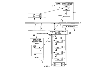
FIG. 7 is a block diagram showing an N x N shared
buffer memory switch which is an embodiment of the present
invention. The functional components which are similar to the
prior art shown in FIG. 2 are denoted by the same reference
numeral, the shared buffer memory switch according to the present
invention has the following functional components:
a shared buffer memory 3 with a large capacity for
temporarily storing cells from any of input ports 11 to any of
output ports 14,
a cell multiplexer 1 for multiplexing incoming cells
through input ports and outputting the multiplexed cells to a
time division multiplex data bus 12, and a cell demultiplexer 7
for demultiplexing and distributing the multiplexed cells on the
time division multiplex data bus 12 to each of output ports,
a shared buffer memory control 10 for controlling
operation of writing cells on a time division multiplex data bus
12 into the shared buffer memory 3 in a writing cycle of the
operation, and reading cells in the shared buffer memory 3 out
to the time division multiplex data bus 12 in a reading cycle of
the operation,
a FIFO (first-in-first-out) memory 4 as an address
pointer queue for storing and indicating address information of
idle areas which are available in the shared buffer memory 3,
2149973
a plurality of FIFO memories 91 to 9N, each of them
corresponding with each of the output ports (from No. 1 to No.
N) to be used as an address pointer queue for indicating an
address information of the shared buffer memory 3 in which the
cell to be routed to the output port has been stored,
a broadcast registration table 6 for the broadcasting
operation and storing the information of broadcasting destina-
tions in the form of bit map data corresponding to each of output
ports, and
a bit map check 8 for checking a bit map data in a cell
at the time of broadcasting operation.
FIGS. 8 and 9 are flowcharts showing a writing
operation and a reading operation of the shared buffer memory
switch respectively according to the present invention, and FIGS .
10(a), (b) and 11 are schematic block diagrams illustrating a
writing operation and a reading operation respectively for a
broadcasting cell according to the present invention. The
operation of the present invention will be described with
reference to those figures.
First, the operation shown in the flowchart of FIG. 8
for the writing operation will be described.
The cell multiplexer 1 multiplexes cells coming through
the input ports 11 and outputs those multiplexed cells to the
time division multiplex data bus 12, and at the same time, the
routing information which shows the destination of each cell,
e.g. output port number to be routed, is transferred to the
shared buffer memory control 10 through the routing information
path 13. The type of cell, e.g. whether it is an ordinary cell
16
2149973
or a broadcasting cell, is also identified by the cell multiple-
xer 1, and this identified information is added to the cell when
it is multiplexed. The VPI and VCI stored in the header of the
cell are used for those operation by the cell multiplexer 1.
The shared buffer memory control 10 writes each cell
in a cell slot, which has already been described relative to the
prior art FIG. 4, on the time division multiplex data bus 12 into
the shared buffer memory one by one in accordance with their
arrival, and all cells in a cell slot group for the input port
are to be written in one cycle of the writing operation.
Therefore, it controls the sequential control of writing in
accordance with the input port number as shown in the steps 510,
S20 and S21 of FIG. 8.
The shared buffer memory control 10 receives the
routing information from the cell multiplexer 1 corresponding to
the cell on the time division multiplex data bus 12 (the step
S11 ) , and also discriminates whether the cell is an ordinary cell
or a broadcasting cell based on the information being added to
the cell (the step S12).
When the cell is an ordinary cell (the step 512: No),
the shared buffer memory control 10 picks up one address
information through the information path 16 from the address
pointer queue of FIFO 4 which manages addresses of the idle areas
available in the shared buffer memory 3 (the step S13), and then
stores the cell in a cell slot on the time division multiplex
data bus 12 into the area of the shared buffer memory 3 which is
indicated by the address information being picked up from the
FIFO 4 (the step S14). The address of the shared buffer memory
17
2149973
3 in which the cell being stored is written into the address
pointer queue of FIFO 9- corresponding to the output port to
which the cell is to be routed through the information path 17
(the step S15).
In the case where the cell is a broadcasting cell (the
step 512: Yes), the shared buffer memory control 10 refers to
the broadcast registration table 6 and extracts the bit map data
which is corresponding to the routing information being received
through the routing information path 13 (the step S16).
As shown in FIG. 10(a), the broadcast registration
table 6 contains the bit map data for all broadcasting cells, and
the bit map data for each of the broadcasting cells is extracted
by indexing the table by the routing information of each
broadcasting cell. The bit map data indicates all destination
for the broadcasting cell by the bit position with "1" corre-
sponding to each output port number.
Then, the shared buffer memory control 10 picks up one
address information available for storing in the shared buffer
memory 3 from the address pointer queue of FIFO 4 ( the step S17 ) .
The bit map data extracted from the broadcast registration table
6 is copied into the cell as shown in FIG. 10(b), and the shared
buffer memory control 10 stores the cell into the area of the
shared buffer memory 3 which is indicated by the address
information being picked up from the FIFO 4 (the step S18). The
address of the shared buffer memory 3 in which the cell being
stored is written into all address pointer queues of FIFOs 9-
corresponding to each output port indicated by the bit map data
for the cell (the step S19). FIG. 10(a) shows an example in
18
~1499'~3
which the destinations for broadcasting the cell are to output
ports No. 2, No. 3, No. 8 and No. 9.
Next, the operation shown in the flowchart of FIG. 9
for the reading operation will be described.
The shared buffer memory control 10 executes the
reading operation in synchronization with each cell slot timing
in the cell slot group for the output port on the time division
multiplex data bus 12, and a cell being stored in the shared
buffer memory 3 is to be read out into the corresponding cell
slot one by one for one cell slot group within one cycle of the
reading operation. Therefore, it controls the sequential control
of reading in accordance with the output port number as shown in
the steps 530, S40 and S41.
The shared buffer memory control 10 reads an address
information written in the address pointer queue of FIFO 9
corresponding to the output port to which the cell is to be read
out, and reads out the cell from the area in the shared buffer
memory 3 with the address indicated by the address information
being read from the FIFO 9- (the steps S31 and S32).
When the cell read out from the shared buffer memory
3 is an ordinary cell (the step 533: No), the shared buffer
memory control 10 puts the cell into the cell slot on the time
division multiplex data bus 12 corresponding to the output port
(the step S34), and proceeds to read a cell for the next output
port.
In the case where the cell read out from the shared
buffer memory 3 is a broadcasting cell (the step S33: Yes), the
bit map data is simultaneously read out together with the cell.
19
2149973
The cell itself is supplied to the cell slot on the time division
multiplex data bus 12 corresponding to the output port (the step
S36). At this time, the shared buffer memory control 10 copies
the cell and resets a bit (set to "0") in the bit map data whose
bit position corresponds to the output port currently being
processed (the step S36), and stores the cell (copied cell) with
the revised bit map data to the same address in the shared buffer
memory 3 through the information path 20 via the bit map check
8.
The bit map check 8 confirms whether any bit in the bit
map data is still set (to "1"), and it allows the cell with the
revised bit map data to be stored in the shared buffer memory 3
if any bit is still set (the step 537: Yes). Having passed the
check by the bit map check 8, the cell with the revised bit map
data is stored in the same address of the shared buffer memory
3 (the step S39).
As the same address of the shared buffer memory 3, in
a
which the cell to be broadcasted is stored, is being written into
all address pointer queues of FIFOs 9- which correspond to the
destination output ports for the broadcasting cell, the shared
buffer memory control 10 can read and outputs the same cell at
the time of reading operation for other output port corresponding
to the broadcasting destination, and the bit map data is revised
(the bits set to "1" are successively set to "0") one by one
whenever the cell for the broadcasting is read out to each
destination.
When the cell has been read out to all output ports for
the destination of the broadcasting operation, all the bits in
2149973
the bit map data are reset to "0" at the step S36 of the reading
operation for the output port in the last turn of the broadcast-
ing, and the bit map check 8 recognizes it as completion of the
broadcasting operation for this cell (the step S38). Then, the
bit map check 8 instructs to the shared buffer memory control 10
that the broadcasting operation has been completed for this
broadcasting cell, and the address used for storing this
broadcasting cell in the shared buffer memory 3 is made idle and
registered to the address pointer queue of FIFO 4 for releasing
the area in which the broadcasting cell was stored.
FIG. 11 shows an example of this reading operation for
the broadcasting cell which is assumed to be routed to output
ports No. 2, No. 3, No. 8 and No. 9. The address "BBB" of the
shared buffer memory 3 in which the cell with the bit map data
is stored is being written into all address pointer queues of
FIFOs 9- for the output ports of the broadcasting destination.
In each time of the cell slot timing for output ports No. 2, No.
3 and No. 8, the address of "BBB" is read and the cell in the
address of "BBB" in the shared buffer memory 3 is read out to the
corresponding cell slot on the time division multiplex data bus
12, and also the copied cell with revised bit map data is stored
into the same address of the shared buffer memory 3 through bit
map check operation by the bit map check 8. At the time of cell
slot timing for the output port No. 9, the same operation
proceeds for reading out the cell to the cell slot for the output
port No. 9 except for storing the cell into the shared buffer
memory 3 because all bits of the bit map data are being set to
"0", and the address of "BBB" being used for storing the cell is
21
2149973
made idle and registered into the address pointer queue of FIFO
4.
Back to FIG. 7, the cell put into the cell slot for the
output port on the time division multiplex data bus 12 is
transferred to the cell demultiplexer 7, and the cell demulti-
plexer 7 demultiplexes the cell on the time division multiplex
data bus 12 and distributes to each output port 14 corresponding
to each cell slot.
As described above, according to the present invention,
when the cell coming through the input port 11 is a broadcasting
cell, it is arranged that the bit map data is read from the
broadcast registration table 6 based on the routing information
for the cell from the cell multiplexer 1, and that the address
for storing the cell into the shared buffer memory 3 is written
into all address pointer queues of FIFOs 9- corresponding to all
output ports for which broadcast output is required as indicated
by the bit map data. Therefore, there is no need to provide the
specific address pointer queue for the broadcasting operation as
in the prior art. As the broadcasting cell is also sequentially
read out and output in response to the read timing of each cell
slot of the output port in the same manner as an ordinary cell,
cells are output in the same order as they are input even if the
ordinary and broadcasting cells are mixed. Therefore, the cell
transfer quality which has originally been defined at the time
of set up operation for each connection can be guaranteed.
Furthermore, it is arranged that the bit map data
relating to the broadcasting cell is stored in the shared buffer
memory 3 together with the cell, and each bit in the bit map data
22
2149973
is reset one by one and stored into the shared buffer memory 3
again whenever the read operation for each output port has
completed, and completion of the broadcasting operation is
recognized by reset of all bits in the bit map data. Thus, the
circuit configuration for processing the broadcasting operation
is simplified and performed at a high speed.
Although the above description is made on a case where
the cell multiplexer 1 performs the discrimination of a cell type
whether it is an ordinary cell or a broadcasting cell and the
result of the discrimination is added to the cell when it is
output to the time division multiplex data bus 12, such a
discrimination may be performed by the shared buffer memory
control 10. Moreover, the routing information may also be
extracted by the shared buffer memory control 10 instead of
receiving from the cell multiplexer 1. This makes the configura-
tion of the cell multiplexer 1 simpler so that the processing
speed can be improved. Still more, the information contained in
the broadcast registration table 6 is not only limited to the bit
map data, but other forms of data which show routing destination
for each broadcasting cell may be available, and the shared
buffer memory control 10 resets the information of each routing
destination one by one whenever it completes the reading
operation for the output port, and also the bit map check 8 can
be altered by other means for recognizing completion of the
reading operation of the broadcasting cell or rather it can be
a part of the shared buffer memory control 10.
Although the present invention has been fully described
by way of the preferred embodiments thereof with reference to the
23
214997
accompanying drawings, various changes and modifications will be
apparent to those having skill in this field. Therefore, unless
these changes and modifications otherwise depart from the scope
of the present invention, they should be construed as included
therein.
24