Note: Descriptions are shown in the official language in which they were submitted.
ATTORNEY ' S DOCKET PATENT APPLICATION
TI-18110
(32350-1078)
~ ~ 2 1 ~ O ~ 4 8
NON-BINARY PULSE WIDTH MODULATION
FOR SPATIAL LIGHT MODULATOR WITH SPLIT RESET ADDRESSINa
TECHNICAL FIELD OF THE INVENTION
This invention relates to spatial light modulators
used for image display systems, and more particularly to
loading spatial light modula'Lors with image data.
ATTORNEY'S DOCKET PATENT APPLICATION
TI-18110
- CA~1~0~4~
BACKGROUND OF THE INVENTION
Video display systems based on spatial light
modulators (SLMs) are increasingly being used as an
alternative to display systems using cathode ray tubes
S (CRTs). SLM systems provide high resolution displays
without the bulk and power consumption of CRT systems.
Digital micro-mirror devices (DMDs) are a type of SLM,
and may be used for either direct-view or projection
display applications. A DMD has an array of micro-
mechanical pixel elements, each having a tiny mirror thatis individually addressable by an electronic signal.
Depending on the state of its addressing signal, each
mirror element tilts so that it either does or does not
reflect light to the image plane. Other SLMs operate on
similar principles, with an array of pixel elements that
may emit or reflect light simultaneously with other pixel
elements, such that a complete image is generated by
addressing pixel elements rather than by scanning a screen.
Another example of an SLM is a liquid crystal display (LCD)
having individually driven pixel elements. Typically,
displaying each frame of pixel data is accomplished by
loading memory cells so that pixel elements can be
simultaneously addressed.
To achieve intermediate levels of illumination,
between white (on) and black (off), pulse-width modulation
(PWM) techniques are used. The basic PWM scheme involves
first determining the rate at whiCh images are to be
presented to the viewer. This establishes a frame rate and
a corresponding frame period. For example, in a standard
television system, images are transmitted at 30 frames per
second, and each frame lasts for approximately 33.3
milliseconds. Then, the intensity resolution for each
pixel element is established. In a simple example, and
assuming n bits of resolution, the frame time is divided
into 2n-1 equal time slices. For a 33.3 millisecond frame
ATTORNEY~S DOCKET PATENT APPLICATION
TI-18110
3 ~A~l 50148
period and n-bit intensity values, the time slice is
33.3/2n-1 milliseconds.
Having established these times, for each pixel of each
frame, pixel intensities are quantized, such that black is
0 time slices, the intensity level represented by the least
significant bit (lsb) is 1 time slice, and maximum
brightness is 2n-1 time slices. Each pixel's quantized
intensity determines its on-time during a frame period.
Thus, during a frame period, each pixel with a quantized
value of more than 0 is on for the number of time slices
that correspond to its intensity. The viewer's eye
inteqrates the pixel brightness so that the image appears
the same as if it were generated with analog levels of
light.
For addressing SLMs, PWM calls for the data to be
formatted into "bit-planes", each bit-plane corresponding
to a bit weight of the intensity value. Thus, if intensity
is represented by an n-bit value, each frame of data has n
bit-planes. Each bit-plane has a 0 or 1 value for each
pixel element. In the simple PWM example described in the
preceding paragraphs, during a frame, each bit-plane is
separately loaded and the pixel elements addressed
according to their associated bit-plane values. For
example, the bit-plane representing the lsb's of each pixel
is displayed for 1 time slice, whereas the bit-plane
representing the MSBs is displayed for 2n-1 time slices.
Because a time slice is only 33.3/255 milliseconds, the SLM
must be capable of loading the lsb bit-plane within that
time. The time for loading the lsb bit-plane is the "peak
data rate".
A high peak data rate puts high throughput demands on
the design of SLMs. To r;ni ize the peak data rate,
modifications to the above-described loading scheme have
been devised. These loading schemes are acceptable only to
ATTORNEY'S DOCKET PATENT APPLICATION
TI-18110
4 CA2 150 1 48
the extent that they minimize visual artifacts in the
displayed image.
One such modification uses a specially configured SLM,
whose pixel elements are grouped into reset groups that are
separately loaded and addressed. This reduces the amount
of data to be loaded during any one time, and permits the
LSB data for each reset group to be displayed at a
different time during the frame period. This configuration
is described in U.S. Patent Serial No. (Atty Dkt No.
TI-17333), assigned to Texas Instruments Incorporated.
ATTORNEY~S DOCKET PATENT APPLICATION
TI-18110
CA21501 48
SUMMARY OF THE INVENTION
One aspect of the invention is a method of displaying
frames of pixel data on a spatial light modulator (SLM)
having individually addressable pixel elements, for a pulse
width modulated display. The invention is useful with any
SLM whose data is allocated parts of the frame period
according to bit-weight. However, the invention is
especially useful for SLM's that use split loading, such as
split-reset addressing, where the number of loads per frame
increases with the number of reset groups, and thus imposes
a minimum number of time slices per frame. For the typical
split-reset SLM, each frame of pixel data is formatted into
bit-planes, each bit-plane having one bit of data for each
of said pixel elements, each bit-plane representing a bit-
weight of said pixel data, and each bit-plane having a
display length that is a part of a frame period. The bit-
planes are sub-formatted into reset groups, each reset
group having data for a group of pixel elements to be
delivered to said SLM at a different time from other pixel
elements, but displayed during substantially the same frame
period. Segments of the display times of one or more of
the more significant of the bit-weights have display
lengths that do not follow a binary pattern. As each
segment or unsegmented bit-plane is loaded, it is displayed
for a display time that is derived from the total of these
non-binary display lengths.
A technical advantage of the invention is that
successfully implements data loading for SLMs having split
loading configurations. The number of loads per frame may
be increased with longer load periods than achieved with
previous methods. Longer load periods ease design
constraints for SLMs.
ATTORNEY~S DOCKET PATENT APPLICATION
TI-18110
6 ~A~ 1501 48
BRIEF DESCRIPTION OF THE DRAWINGS
Figures 1 and 2 are block diagrams of image display
systems, each having an SLM that is addressed with a split-
reset PWM data loading method in accordance with the
invention.
Figure 3 illustrates the SLM of Figures 1 and ~,
configured for split-reset addressing.
Figure 4 illustrates an example of displaying pixel
data in accordance with the invention.
Figure 5 illustrates another example of displaying
pixel data in accordance with ~he invention.
ATTORNE;Y'S DOCKET PATENT APPLICATION
TI-18110
7 CA~1$~4~
DETAILED DESCRIPTION OF THE INVENTION
Overview of SLM Displa~ Systems Usinq PWM
Comprehensive descriptions of DMD-based digital
display systems are set out in U.S. Patent No. 5,079,544,
entitled "Standard Independent Digitized Video System"; ~in
U.S. Patent Serial No. (Atty Dkt No. TI-17855), entitled
"Digital Television System"; and in U.S. Patent Serial No.
(Atty Dkt No. TI- 17671), entitled "DMD Display
System". Each of these patents and patent applications is
assigned to Texas Instruments Incorporated, and each is
incorporated by reference herein. An overview of such
systems is discussed below in connection with Figures 1 and
2.
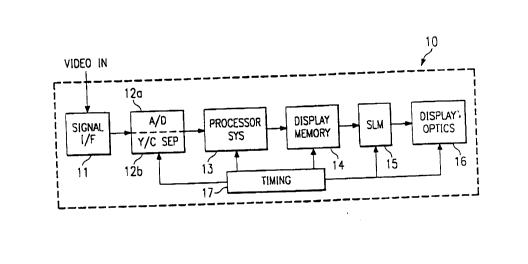
Figure 1 is a block diagram of a projection display
system 10, which uses an SLM 15 to generate real-time
images from a analog video signal, such as a broadcast
television signal. Figure 2 is a block diagram of a
similar system 20, in which the input signal already
represents digital data. In both Figures 1 and 2, only
those components significant to main-screen pixel data
processing are shown. Other components, such as might be
used for processing synchronization and audio signals or
secondary screen features, such as closed captioning, are
not shown.
Signal interface unit 11 receives an analog video
signal and separates video, synchronization, and audio
signals. It delivers the video signal to A/D converter 12a
and Y/C separator 12b, which convert the data into pixel-
data samples and which separate the luminance ("Y") datafrom the chrominance ("C") data, respectively. In Figure
1, the signal is converted to digital data before Y/C
separation, but in other embodiments, Y/C separation could
be performed before A/D conversion, using analog filters.
CA~ 1 50 1 48
ATTORNEY'S DOCKET PATENT APPLICATION
TI-18110
Processor system 13 prepares the data for display, by
performing various pixel data processing tasks. Processor
system 13 includes whatever processing memory is useful for
such tasks, such as field and line buffers. The tasks
performed by processor system 13 may include linearization
(to compensate for samma correction), colorspàce
conversion, and line generation. The order in which these
tasks are performed may vary.
Display memory 14 receives processed pixel data from
processor system 13. It formats the data, on input or on
output, into "bit-plane" format, and delivers the bit-
planes to SLM 16 one at a time. The bit-plane format
permits each pixel element of SLM 15 to be turned on or off
in response to the value of 1 bit of data at a time. In a
typical display system 10, display memory 14 is a "double
buffer" memory, which means that it has a capacity for at
least two display frames. The buffer for one display frame
can be read out to SLM 15 while the buffer another display
frame is being written. The two buffers are controlled in
a "ping-pong" manner so that data is continuously available
to SLM 15.
As discussed in the Background, the data from display
memory is delivered in bit-planes to SLM 15. Although this
description is in terms of a DMD-type of SLM 15, other
types of SLMs could be substituted into display system 10
and used for the invention described herein. For example,
SLM 15 could be an LCD-type SLM. Details of a suitable SLM
15 are set out in U.S. Patent No. 4,956,619, entitled
"Spatial Light Modulator", which is assigned to Texas
Instruments Incorporated, and incorporated by reference
herein. Essentially, DMD 15 uses the data from display
memory 14 to address its pixel elements. The "on" or "off"
state of each pixel element in the array of DMD 15 forms an
lmage.
` -
ATTORNEY'S DOCKET PATENT APPLICATION
TI-18110
g ~A~ 5~
U.S. Patent No. 5,278,652, entitled "DMD Architecture
and Timing for Use in a Pulse-Width Modulated Display
System", describes a method of formatting video data for
use with a DMD-based display system and a method of
addressing them for PWM displays. This patent application
is assigned to Texas Instruments Incorporated, and ~is
incorporated herein by reference. Some of the techniques
discussed therein include clearing blocks of pixel
elements, using extra "off" times to load data, and of
breaking up the time in which the more significant bits are
displayed into smaller segments. These techniques could be
used for any SLM using PWM.
Display optics unit 16 has optical components for
receiving the image from SLM 15 and for illuminating an
image plane such as a display screen. For color displays,
the bit-planes for each color could be sequenced and
synchronized to a color wheel that is part of display
optics unit 16. or, the data for different colors could be
concurrently displayed on three SLMs and combined by
display optics unit 16. Master timing unit 17 provides
various system control functions.
Split Reset Addressinq
Figure 3 illustrates the pixel element array of SLM
15, configured for split-reset addressing. Only a small
number of pixel elements 31 and their related memory cells
32 are explicitly shown, but as indicated, SLM 15 has
additional rows and columns of pixel elements 31 and memory
cells 32. A typical SLM 15 has hundreds or thousands of
such pixel elements 31.
In the example of Figure 3, sets of four pixel
elements 31 share a memory cell 32. As explained below,
this divides SLM 15 into four reset groups of pixel
elements 31. The data for these reset groups is formatted
into reset group data. Thus, where p is the number of
ATTORNEY'S DOCKET PATENT APPLICATION
TI-18110
lo ~ A ~
pixels and q is the number of reset groups, a bit-plane
having p number of bits is formatted into a reset group
having p/q bits of data. The reset groups are divided
"horizontally" in the sense that every fourth line of pixel
elements 31 belongs to a different reset group.
U.S. Patent Serial No. (Atty Dkt No. TI-17333~,
entitled "Pixel Control Circuitry for Spatial Light
Modulator", assigned to Texas Instruments Incorporated and
incorporated by reference herein, describes split-reset
data loading and addressing for a DMD. These concepts are
applicable to SLMs in general.
Figure 3 illustrates how a single memory cell 32
serves multiple pixel elements 31. Pixel elements 31 are
operated in a bistable mode. The switching of their states
from on to off is controiled by loading their memory cells
32 with a bit of data and applying a voltage indicated by
that bit to address electrodes connected to the pixel
elements via address lines 33. Then, the state of the
pixel element 31 is switched, in accordance with the
voltage applied to each, by means of a reset signal via
reset lines 34. In other words, for each set of four pixel
elements 31, either 1 or a 0 data value is delivered to
their memory cell 32, and applied to these pixel elements
31 as a "+" or "-" voltage. Signals on the reset lines 34
determine which pixel element 31 in that set will change
state.
One aspect of split-reset addressing is that only a
subset of the entire SLM array is loaded at one time. In
other words, instead of loading an entire bit-plane of data
at once, the loading for reset groups of that bit-plane's
data occurs at different times within the frame period. A
reset signal determines which pixel element 31 associated
with a memory cell 32 will be turned on or off.
The pixel elements 31 are grouped into sets of four
pixel elements 31, each from a different reset group. Each
ATTORNEY'S DOCKET PATENT APPLICATION
TI-18110
11 C~ O ~ ~
set is in communication with a memory cell 32. In the
horizontal split reset example, pixel elements 32 from each
of the first four lines, each belonging to a different
reset group, share the same memory cell 32. The pixel
elements 31 from each of the next four lines would also
share memory cells 32. The number of pixel elements ~31
associated with a single memory cell 32 is referred to as
the "fanout" of that memory cell 32. The fanout could be
some other number. A greater fanout results in the use of
fewer memory cells 32 and a reduced amount of data loading
within each reset period, bu~ requires more resets per
frame.
In each set of four pixel elements 31, four reset
lines 34 control the times when the pixel elements 31
change state. Each pixel element 31 in this set is
connected to a different reset line 33. This permits each
pixel element 31 in a set to change its state at a
different time from that of the other pixel elements 31 in
that set. It also permits an entire reset group to be
controlled by a common signal on its reset lines 34.
Once all memory cells 32 for the pixel elements 31 of
a particular reset group have been loaded, the reset lines
34 provide a reset signal to cause the states of those
pixel elements 31 to change in accordance with the data in
their associated memory cells 32. In other words, the
pixel elements 31 retain their current state as the data
supplied to them changes, and until receiving a reset
signal.
PWM addressing sequences for split-reset SLM's are
devised in accordance with various heuristic rules. one
rule is that the data for no more than one reset group can
be loaded at the same time. In other words, the loading of
different reset groups must not conflict. Other "optional"
rules are described in U.S. Patent Serial No. (Atty
ATTORNEY'S DOCKET PATENT APPLICATION
TI-18110
12 ~A~1501~8
Dkt No. TI-17333), assigned to Texas Instruments
Incorporated and incorporated by reference herein.
Non-BinarY PWM
A feature of the invention is the recognition that PWM
for SLMs need not follow binary constraints. In other
words, for a system with a pixel resolution of n-bits per
pixel, the number of time slices allocated for displaying
bit-planes of varying bit-weights need not follow a 2n-1,
10 2n-2, 2n-n pattern, as has been the case with
conventional PWM methods. I.,stead, the number of time
slices for the bit-planes can be determined by other system
requirements. Also, the number of time slices per frame
period is not necessarily 2n-1.
Pixel resolution is only one of several system
requirements to be considered in determining allocation of
time slices. Another system requirement to be considered
is the split reset fanout. For purposes of example in this
description, a fanout of 16 reset groups is assumed. Thus,
as explained above, the data for each bit-plane is
formatted so that it can be loaded in 16 different groups.
A third system requirement to be considered is the
number of loads per frame. U.S. Patent No. 5,278,652,
referred to above, and U.S. Patent Serial No. (Atty
Dkt No. TI-18384), entitled "Pulse Width Modulation for
Spatial Light Modulator with Split Reset Addressing",
assigned to Texas Instruments Incorporated and incorporated
by reference herein, both describe a method of dividing the
display times of the bit-planes of the more significant
bits into segments. The bit-planes selected for
segmentation could be any one or more of the bit-planes
other than that of the lsb. Typically, the segments are of
equal duration, but this is not necessary. For each
segmented bit-plane, the display of its segments is
distributed throughout the frame period. When the SLM has
ATTORNEY'S DOCKET PATENT APPLICATION
TI-18110
13 C A ~ l ~ r ~
split-reset addressing, typically, each reset group is
segmented in the same manner, and its segments displayed in
the same basic pattern as those of the other reset
groups.
The number of loads per frame is the number of
segments plus the number of unsegmented bit-planes, times
the number of reset groups. For example, if the 4 more
significant bits of 8-bit pixel data are segmented into 8,
4, 2, and 1 segments, respectively, the number of loads per
frame is (8+4+2+1+1+1+1+1) * 16 = 304.
The number of loads per 'rame cannot exceed the number
of time slices per frame. Also, to permit the highest bit
weight to represent half intensity, the number of loads
must be encodable with the pixel resolution. Thus, for 8-
bit pixel data, the segmentation scheme of the preceding
paragraph cannot be accomplished if the conventional 2n-1
time slices per frame are used, because 304 is greater than
28-l = 255.
However, if the pixel resolution is increased to 9-
bits, the segmentation scheme can be accomplished.
Although the number of loads per frame increases by one
load per reset group, or (8+4+2+1+1+1+1+1+1) * 16 = 320,
this number of loads is encodable with 9 bits. As
explained below, the number of time slices per frame is
derived from this number of loads, rather than by a 2n-1
constraint.
As indicated in the Background, a characteristic of
PWM on SLM's is that display times are allocated in terms
of "time slices" per frame period. Because the bit-plane
representing the lsb is loaded and displayed during a
single time slice, a time slice is often referred to as a
"lsb period". The duration of a time slice, in units of
time, is determined by dividing the frame period by the
number of time slices. The "display lengths" referred to
herein are in terms of the number of time slices allocated
ATTORNEY'S DOCKET PATENT APPLICATION
TI-18110
14 C A2~0il48
to a particular segment of a bit-plane or to an unsegmented
bit-plane, and the "display times" are each a product of a
number of time slices times the lsb period.
To determine the number of time slices per frame, and
hence the duration of a lsb period, the minimum display
length of each segment is determined. This minimum displày
length may be determined by dividing the number of loads
per frame by the number of segments of the more significant
bits, as follows:
segment display length = 320/8+4+2+1
= 21.33
The truncated result, 21, is the minimum number of "lsb
periods" allocated to each segment. The segment length
could be longer than the number of loads divided by the
number of segments, but for purposes of example, herein, a
segment display length of 21 lsb periods is assumed.
The display lengths of the 5 less significant bits can
be allocated in any manner that represents 5 levels of
intensity less than the segment display length. For
optimum light efficiency, the total of the 5 display
lengths of these less significant bits should equal the
segment length minus one lsb period. In the example of
this description, the 5 less significant bits are weighted
between 0 and 20. One such weighting is 8, 5, 4, 2, and 1,
which represent the lsb periods for bits 4-0, respectively.
The minimum number of lsb periods per frame can now be
determined from the sum of all segment lengths and
unsegmented bit-plane lengths. In the example herein:
N = (8*21)+(4*21)+(2*21)+21+8+5+4+2~1
= 335 lsb periods
The frame period can now be divided into time slices.
Typically, for optimum light efficiency, the number of time
slices is the same as the total display length, N lsb
periods. Thus, in the example herein, for a frame period
of T, each time slice is T/335. However, it is possible to
ATTORNEY'S DOCKET PATENT APPLICATION
TI-18110
add extra time slices per frame, for various purposes, such
as the "off lsb periods" described in U.S. Patent No.
5,278,652. In any event, the total display length, here
335, is the minimum number of time slices per frame.
Figures 4 and 5 illustrate two examples of a method of
displaying data for PWM on a split-reset SLM. This meth~d
includes the division of a frame period into time slices in
accordance with the invention. As described above, the
number of lsb periods is determined essentially by the
number of loads per frame. In these examples, the number
of time slices is the same as che number of lsb periods.
In Figure 4, the display lengths for the more
significant bits (bits 5 - 7) are segmented and the
segments are distributed throughout the frame period. The
display lengths of the less significant bits (bits 0 - 4)
are not segmented and are loaded and displayed during the
middle of the frame period. Typically, each reset group is
displayed in this same sequence, with the loading of each
reset group being staggered by one time slice to avoid
conflicts. The exception is the unsegmented display
lengths (bits 0 - 4), whose loading sequence may vary among
reset groups to avoid conflicts. However, this is not a
requirement of the invention, and the loading sequence
could vary from reset group to reset group. -
Figure 5 illustrates a second example of a method of
split-reset PWM addressing in accordance with the
invention. As in Figure 4, for each reset group, segments
and unsegmented display lengths are displayed for a
predetermined number of time slices. However, the
displaying of data for the less significant bits occurs
throughout the frame period instead of being concentrated
in mid-frame.
ATTORNEY'S DOCKET PATENT APPLICATION
TI-1~110
16 CA~1~01~8
Other Embodiments
Although the invention has been described with
reference to specific ~mbodiments, this description is not
meant to be construed in a limiting sense. Various
modifications of the disclosed embodiments, as well as
alternative embodiments, will be apparent to persons
skilled in the art. It is, therefore, contemplated that
the appended claims will cover all modifications that fall
within the true scope of the invention.