Note: Descriptions are shown in the official language in which they were submitted.
21S06 35
CURRENT MEASUREMENT CIRCUIT
COMPRISING A MUTUALLY COUPLED TRANSFORMER
AND AN INTEGRATION CIRCUIT
s The present invention concerns a current measurement circuit
comprising a mutually coupled transformer and an integration
circuit which integrates the signal of the mutually coupled
transformer.
10 The use of mutually coupled transformers (otherwise known
as inductively coupled transformers) for measuring currents
possesses certain advantages in comparison with other
measuring devices. In particuler, in the field of electricity
metering, the use of a mutually coupled transformer avoids
s the problems of saturation by dc currents which arise with
iron-core transformers and enables the measurement of the
current separately from other measurements, for example
measurements of the current on the other phases of a
multiphase network. However, mutually coupled transformers
2 o present a particular problem in that the signal supplied by the
transformer is the derivative of the measured current. Thus,
the use of a mutually coupled transformer requires an
integration circuit to process the signal.
2 s A measurement circuit including a mutually coupled
transformer and an integration circuit are described in the
patent application EP 0 403 330. The integration circuit of this
application is particularly adapted to suppress low frequency
signals and parasitic dc signals which can be produced at the
3 o output of conventional integration circuits.
It is often the case that signals representing a measurement of
current are converted by an analogue digital converter for
later processing. A known technique for improving the
3 s resolution of an analogue digital converter uses a dither signal
added to the measured signal before conversion by the
- 21~0~3S
converter. This dither signal can be a random signal or a
periodic signal, for example a triangular signal or a signal
having the form of a ramp. Using this technique the value of
the measured signal can be determined by an analysis of the
s converted values of the signal with a resolution finer than that
normally possible with the available quantisation steps of the
converter. The principals of the dither technique have been
known for a long time and examples of measurement and
communication systems which use a dither signal for
o improving the performance of a converter are described in
US 4 187 466, EP O 181 719 and EP O 613 256. The patent
EP O 181 719 in particular describes the principles of a system
which adds a triangular dither signal to the current signal
before conversion.
It is thus desirable to have a system for measuring currents
which combines the advantages associated with a mutually
coupled transformer with those associated with the use of a
dither signal. The generation of a dither signal can present
2 o problems in relation to the cost of components and the
complexity of the system which generates it. The present
invention aims to provide a system which provides the
advantages of the two techniques but which avoids the
problems of complexity and duplication of components.
2s
To this end, the present invention is characterized in that the
measurement circuit further comprises a dither circuit which
adds a substantially rectangular signal to the signal from the
transformer before the input of the integration circuit in order
3 o that the integration circuit provides a signal representing the
measured current perturbed by a substantially triangular
dither signal.
In general, a square wave or rectangular signal is not
3 s appropriate as a dither signal but it may be easily generated in
an electronic circuit, for example, at the output of a
2150~3~
microprocessor. The present invention provides a circuit in
which a current signal modulated by a triangular dither signal
is produced and which can be sent to an analogue to digital
converter, but which avoids duplication of components due to
5 the fact that the integration circuit performs both the functions
of integration of the signal from the mutually coupled
transformer and of creation of a dither signal.
As described above, the value of the measured signal by the
o transformer may then be calculated after conversion by the
steps of signal processing with a resolution finer than that
possible with only an analogue to digital converter.
The integration circuit may be a digital or analogue integrator
of a conventional type. However, preferably, a circuit similar to
that of EP O 403 330 is used, which comprises an ~mplifier
having an associated gain resistance and a feedback loop, the
feedback loop comprising a feedback capacitor, the integration
circuit further comprising a second integrator mounted at the
2 o output of the amplifier, upstream of the feedback loop.
By these means, the integration circuit suppresses low
frequencies and parasite dc signals which can arise in
conventional analogue circuits. Preferably, the integration
2 5 ciricuit can further comprise means for correction of the phase
delays in the integratd signal, in particular the delay
introduced by the gain resistance of the integrator, comprising
a passive filter mounted upstream of the amplifier. Where the
current measurent circuit forms part of the input circuit of an
3 o electricity meter, including a voltage measurement circuit, the
passive filter can be dimensioned in order that all the phase
delays between the voltage and current paths are corrected by
this filter, the voltage in the network being measured directly
without changing its phase. Thus, the voltage channel is free
3 5 from constraints regarding the use of components used for
correction of phase, which is advantageous if the voltage
~laO63~ -
channel is also used for communication of data.
As discussed above, a square wave or rectangular signal is
easily generated by an electronic circuit. In one embodiment,
5 the rectangular signal can be generated using a pulse width
modulated signal (PWM), provided at an output of a
microprocessor, which signal is passed via a switching means
comprising at least one latch in order to divide the average
frequency of the PWM signal and to create the square wave.
The use of a dither signal having the form of a simple
triangular waveform can cause problems associated with the
relation between the amplitude of the signal and the
quantisation steps of the converter. In particular, a problem
arises if the amplitude of the dither signal is not equal to an
integral number of quantisation steps of the converter. In
order to overcome these problems, the dither circuit
preferably supplies a rectangular signal which is further
modulated by a modulation signal. This signal is then
2 o integrated in order to become a modulated triangular signal.
The use of a signal having this form overcomes the problems
associated with the differences between the amplitude of the
non-modulated triangular signal and the quantisation levels of
2 s the converter. In effect, the modulation signal introduces a
component to the converted values which is dependant on the
differences between the amplitude of the triangular signal and
the quantisation steps of the converter and which can be
suppressed after conversion in the same processing operation
3 o that suppresses the dither signal, for example, by using a
decimation filter.
Preferably, the modulation signal is also generated using the
PWM signal of the microprocessor. In one embodiment, the
3 5 two limits of the modulation signal may be generated using
two integrating circuits which integrate the PWM signal (and
2150~3~
its inverse) in order to create each limit. However, it is possible
to further reduce the number of components used. Preferably,
the dither circuit comprises an integrator which integrates the
pulse width modulated signal in order to create a triangular
5 signal representing one limit of the modulation signal, this
signal being supplied to switching means in order to create a
substantially rectangular signal having only one limit which
varies as per the signal from the integrator, the dither circuit
further comprising a filter which filters low frequency
o components from the signal so as to provide a rectangular
signal which is symetrically modulated.
Considering the rectangular modulated signal before the
filtering step, this signal comprises a frequency component
corresponding to the frequency of the rectangular signal and a
low frequency component corresponding to the triangular
signal which modulates one of the two limits of the rectangular
signal. The filter thus eliminates low frequency components
and the signal assumes a symetrical shape, i.e. such that the
2 o two limits of the signal are equally modulated.
The invention will be best understood in the light of the
following description of one embodiment of the invention,
which is given by way of an illustrative and non-limiting
2 5 example, with reference to the attached drawings in which
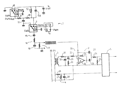
Figure 1 shows an example of an input circuit for an electricity
meter comprising a current measurement circuit as per the
present invention;
Figure 2 shows the steps of creation of the dither signal added
to the current signal measured by the circuit of Figure 1.
As is shown in Figure 1, the input circuit for an electricity
3 5 meter as per this embodiment comprises a current
measurement circuit including a dither circuit 1 and an
215063~
integrating circuit 2, which integrates the signal from an
inductance transformer 3 (mutually coupled transformer)
combined with a square wave supplied by the dither circuit, a
voltage measurement circuit 4 and an analogue to digital
s converter S.
The dither circuit 1 comprises a latch 6 which receives the
PWM signal of a microprocessor associated with this circuit.
The latch divides the average frequency of the PWM signal in
o order to create a square wave. The modulation signal is
produced by the switch 8 which cuts the reference voltage
Vref in response to the PWM signal of the microprocessor, so
as to produce, after filtering by the resistance and capacitor 9
and 11 and addition of the reference voltage Vref by the
15 resistances 9, 10 and 12, the modulated Vref signal. This signal
is modulated in a triangular form at the frequency of the PWM
cycle and having a depth of modulation which is dependant on
the relation R 12
R9 + R10
This signal is then cut by the second switch 7 in response to
the square wave produced by the PWM signal passed via the
latch 6 so as to provide an assymetrically modulated square
wave signal. The capacitor 13 serves to equalise the rise and
2 s fall times of the modulation signal.
As shown in Figure 1, this signal, modulated at its upper limit,
is treated by a symetrising circuit comprising a capacitor 15,
which eliminates the low frequencies which render the
3 o modulated square wave assymetric so as to generate a
trapezoidally modulated square wa~e, and resistances 16, 17
and a capacitor 18 which function to compensate for the
distortion of the trapezoidal signal output from the capacitor
lS. In effect, the symetrising circuit comprising the
3 5 components 15 to 18 constitutes a pass band filter, which
passes the frequency of the square wave and its first
215063~
harmonics and which excludes the frequences which distort
the symetrical form of the signal. Referring to Figure 2 a
square wave signal modulated and symetric is thus produced.
5 As shown in Figure 1 the current measurement circuit further
comprises a mutual inductance transformer 3, the signal of
which represents the derivative of the current which passes in
the phase F1 of an a.c. network. This signal is supplied to the
integrator circuit 2 and after to the analogue-digital converter
o 5. The integration circuit 2 comprises an amplifier 20 having a
feedback loop formed of a capacitor 21 and a resistance 22
which control the integration of the signal of the transformer.
The circuit further comprises a coupling capacitor 23
connected at the output of the amplifier upstream of the
feedback loop, which changes the characteristics of the circuit
in order to suppress low frequencies and dc signals, and a gain
limiting resistance 24 which prevents the saturation of the
amplifier. A voltage divider 24, 25 is connected at the output
of the circuit upstream of the converter 5. In effect, these
2 o elements of the circuit correspond to the circuit described in
EP 0 403 330 which supplies a signal corresponding to the
integral of the signal of the transformer without parasitic
effects and distortions of the signal.
2 5 The current measurement circuit forms part of an input circuit
of an electricity meter which further comprises a voltage
measurement circuit 4, comprising a voltage divider comprised
of two resistances 26, 27. The input circuit of the present
invention is different from that of the circuit of EP 0 403 330
3 o in that there is no phase correcting element in the voltage
signal path, the capacitor 28 functioning only to attenuate
undesired high frequencies. That is, the phase correction
elements are formed by the capacitor 29 and the resistance 30
which function in combination with the resistances 22 and 31
3 5 to correct the phase in the current path so that the current and
voltage paths are in phase at the input of the analogue to
2150635
digital converter. The current path further comprises a
capacitor 32 which attenuates undesired high frequencies. The
capacitors 28 and 32 are optional and may be omitted in other
embodiments .
s
The signal from the dither circuit is added to the signal
received from the transformer 3 and supplied to the
integration circuit at the point 33. The combination of the
signals is then integrated in order to create a signal
o representing the image of the current measured by the
transformer dithered by a dither signal having the form of a
triangular waveform modulated by a trapezoid. The amplitude
of the waveform and of the modulation signal are chosen to
create a dither signal comprising a triangular signal 30 having
an amplitude corresponding to several quantisation steps of
the converter modulated at each limit by an amplitude
corresponding to at least half a quantisation step. The signal is
then supplied to the input of the analogue to digital converter.
As described in the introduction above, the use of a signal
2 o having this form improves the resolution of the signal by the
converter. After the step of conversion the dither signal can be
removed using a digital decimation filter or other known
means, for example, by the conversion of the anlogue dither
signal to a digital signal and the subtraction of this signal from
2 s the signal representing the combined values of the current and
dither signal. The current and voltage signal thus calculated
can be used in a calculation of the energy consumed etc.