Note: Descriptions are shown in the official language in which they were submitted.
~WO95112253 21 S O ~18 PCT/US94/1032~
Automatic Frequency Control Apparatus
Field of the Invention
This invention relates to ~ntQm~tic frequency control (AFC)
and more spe~ific~lly to adjusting the frequency of an osrill~tor
based on received data such that the frequency of oscill~tion is
synchronized to an external ~efelellce.
1 5 Back~.,ulld of the Invention
In the GSM (Global System for Mobile Communications)
standard of digital celllll~r telephony a large number of mobile
st~tiC~ can commllnic~te with a netwul~ of base stations. The
2 0 mobile stations decode data from the base station nelwolk in
digital form and, among many other functions, use this data to
periodically adjust the master ~efe.ellce os-.ill~t~r frequency of the
mobile station.
Cl~ lly this adjustment of the master lefelellce osr.ill~tor
2 5 frequency has been performed by using a digital to ~n~log
c.ll~ er to change the digital frequency correction data into
s3n~10g form and then applying the resulting ~n~log signal to a
varactor diode to warp a crystal lefelellce osr~ tor.
WO 95/12253 PCT/US94/1032~ ~
21S~818
This method has several shol Ir,o~in~. First of all the
frequency correction data is already in digital form in the GSM
system. It would be desirable to use the data in digital form and
thus elimin~te the digital to ~n~log COllvt:l Ler.
Secondly, using a varactor diode to warp a crystal results in a
non-linear tuning characteristic. This requires a complex
pll~.cing algorithm to linearize the characteristic.
Finally, the practical limit~tio~.~ of the digital to analog
collvt:l lar resolution and the crystal oscill~tor component
l O tolerances require a fairly large step size in the frequency tuning
characteristic. In the GSM ~y~L~ this results in a step size of
about 50Hz. Since the frequency accuracy of GSM is required to be
<lOOHz this can be a major problem.
A digital ~lltom~tic frequency control sy~Lelu can be realized
1 5 by the use of frAction~l N synthesi.~. Such a :~y~Lell- is shown in
U.S. Patent # 5,111,162, entitled "Digital Frequency Synth~si~er
having AFC and Mol11l1~tio~ Applied to Frequency Divider"
~llthored by Hietala et al. In this patent a secQr~ ry divider is
used from the main oscill~tor output to derive a low frequency
2 0 lefe~ellce for offset synthesi~:ers and logic cil.;Ui~y. This
secor -l~ry divider operates at the output frequency, thus, draws
~rcesaive current.
Thel~o~e it would be advantageous to devise a digital
~llt~m~tic frequency control sy~L~m which allows the digital
2 5 aut~m~t;c frequency control data to be used without co,lv~l~ion to
An~log form while providing a linear tuning characteristic with
very fine minimllm frequency step size and without drawing
e~cessive current.
2150818
~WO 95/12253 PCT/US94/1032~
Description of the Drawings
FIG. 1 is an illustration in block diagram form of a
radiotelephone transceiver in accordance with the present
invention.
FIG. 2 is an illustration in block diagram form of a
radiotelephone transceivt:r in accordance with the present
1 0 invention.
FIG. 3 is an illustration in block diagr~m form of a
synthesi7er section of a radiotelephone transceiver which is
~p~hle of ~ lrul~ing the digital autom~tic frequency control in
accordance with the present invent,io~
1 5
Description of a I'rerel.ed Embo~liment
The ~-efe..ed embo~iment of the present illvellLion
2 0 encomr~ses a digital ~ntom~tic frequency control ~,y~Le~
implemant,e-1 in a radiotelephone. The radiotelephone includes a
frequency synthe~i~er in which a variable oscill~tor output is fed
to a ~ligit~l divider. The division ratio of the digital divider is
varied with time by a multi accnmtll~tor fractional N division
2 5 sy~,Lelll such that the erre.iLive division ratio may be varied by non-
integer steps. The division ratio is then l lo~,".. -e-l to realize
the desired ch~nnel frequency, the desired modulation waveform,
and any ~lltom~tic frequency correction offset. The ouLl~ut of the
WO 95/122S3 PCT/US94/1032~ ~
~1~iO~
digital divider feeds one input of a phase comp~ri~o~ neLwulk.
The other input of the phase comp~rison nelwulk is fed from a
reference oscill~tor. The phase comparison neLwolh ouL~-lL is
filtered to remove extraneous noise components and is then fed to
5 the control input of the variable osrillAt~r. The control input is
such that the variable osçill~tor uuL,u~lL frequency will adjust itself
until it is equal to the ~erel~llce oscill~tQr frequency multiplied by
the digital division ratio. This results in a digital alltom~tic
frequency col.~clion input port with t,~LL,e~ely fine resolution.
10 Additionally, the lere~ .ce osrill~tnr does not need to be warped by
a varactor diode in this sit~l~tion~ thus, the lefele:llce oscillator is a
free rl-nninE crystal osrill~tor with accuracy only a~u~u~o~ ating
the expected ~ ~Çe~llce frequency.
In the GSM sy~L~ , the clock signal used to drive the logic
1 5 sections of the radio is required to be synchronized to the radio
frequency ouLl uL ~iEn~l Thelerole, the free rllnninE crystal
oscill~tor cannot be used directly as the clock to the logic sections
of the radio. An accurate clock is provided to the logic sections of
the radio and to the ~eft~ ce inputs of any offset synt~esi~rs of
2 0 the radio by using a second multiple ~ccllm~ t~r fractional N
division L;y~Lelu to divide the in~c~ ~.ate ~efe.ellce osrill~tor
frequency down to a fixed ac. ~ate frequency. This seco~-l
fr~qctior-~l N division ~y~jle~ is ,ulo~ llme~l based on the
allt~m~tic frequency control progr~mmin~ of the first fractional N
2 5 division system . This lower frequency may then be mllltiplie-l in
a phase locked loop to provide an accurate l~resellce at the
origin~lly desired ~efel~llce frequency if necessary.
2150~18
~WO 95/12253 PCTIUS94/10324
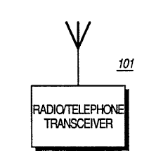
FIG. 1 is an illustration in block diagram form of a
radiotelephone 101. The radiotelephone 101 may be, but is not
limited to be, a cellular radio telephone employing the GSM
standard of opeld~ion. In Figure 2 the radiotelephone 101 is
shown to be composed of a trAncmitter 102, a receiver 103, a
control y~l~ 104, a user interface 105, and a syn~ esi7~r 107.
The syT~th~,ci7er 107 provides the l~eiver 103 and the transmitter
102 with .cign~lc, tuned to the proper frequency, to allow the
reception and tr~ncmiccion of data from user interface 105. In
1 0 addition the syntheci7er 107 provides the user interface 105 and
the control logic 104 with the necessAry clock signal for proper
operation of the logic ~ihcui~s co..t~i..etl within these blocks. The
user interface 105 typically in~ les a microphone~ a speAk~r, a
display and a keypad.
1 5 One of t,he filnctionc of control logic 104 is to derive a digital
signal from data r~eived by l~eivt:r 103 to be used to adjust the
frequency of synt.h~.ci7er 107. This digital signal is known as
autom~tic frequency control.
With le~ ce to Figure 3 the Alltom~tic frequency control
2 0 signal is applied to data port 114 in a serially lo~Aerl form known
as the serial progrAmmin~ il,telrace (SPI) form. The serial data
is l-)Atle~ into latch 117 in which it is collv~rted to parallel form
and is then applied to adder 118. Two other inputs are applied to
adder 118. The fractional part of the division to set the ~h~nnel
2 5 frequency is input to data port 113 in SPI form from control logic
104. This data is converted into parallel form by latch 116 and is
then input to adder 118. The modulation is input to serial data
port 11~. Look-up read only m~mory (ROM) 119 traces out
_
WO 95/12253 PCT/US94/10324 ~
21508~8
frequency versus time patterns depPn-lant on the serial data
stream leceived at port 116. The oul~ul of read only memory 119 is
then input to adder 118.
The output of adder 118 is then used as the data input to
accumulator 120. A cACc~a of AccllmlllAtors (121, 122, and 123~
along with recomhinAtion logic 124 form a time varying sequence
which is added to the non-frArtion~l part of the division in adder
126. The resulting sequence is then used to control divider 109.
The divider control sequence results in effective division ratios
1 0 which allow the syntheRiqer to realize fine frequency steps without
a~reSRive spurious col-tel-t in the synt~aRi~er out~u~ 138. The
divider control sequence co..t~ all il,fo~ l~,ation of ~h~nnel
setting, mntllllAtion, and AlltomAt.ic frequency control. ( For a
detailed a~rlAnAtion of this result see U.S. Patent #5,093,632
1 5 entitled "T.Atr.hetl ~cllmnl~tQr Fr~io~l N Syntha~i~ with
Residual Error Correction" authored by Hietala et al or U.S.
ratell~ #5,166,642 entit!erl "Multiple ~cllmlllAtor FrAc~iorlAl N
SyntheRiR with Series RecomhinAt;on" Alltl~ored by Hietala)
The uul~uul of divider 109 is used to provide the internal clock
2 0 of the fr~ctionAl N syn~aRiser 140 consisting of Accllmlll~tQrs 120,
121, 122, and 123, recomhinAtion logic 124 and look-up ROM 119.
~litionAlly, the c~uL~uul of divider 109 is input to phase ~lal~ - 110
where its phase is comr~red to that of r~ lce oscillAtQr 127.
The ou~l of phase detector 110 drives charge pump 111 which in
2 5 turn drives the loop filter 112. The loop filter 112 develops a voltage
to control the voltage sensitive port of variable osrillAtQr 108.
Finally, the ûul~uut of variable osrill~tor 108 is used as the
srt~ eSi7er ~ ul~-ll 138 and is provided to leceivel 103 and
~WO 9S/12253 215 0 ~ 18 PCTIUS9411032~
tr~n.cmitter 102 and also is provided to the input of divider 109 to
complete the phase locked loop.
In the ~lefelled embotlim~nt the ~lltom~tic frequency
control is provided to port 114 instead of directly to the reference
S osr.ill~tor 127. Thus, the accuracy of the reference os~.ill~tor 127 is
m~i..t~i~.e~1 only by the stability of crysW 128. Any inaccuracy of
crysW 128 due to tempeldl,ule, make tolerance, or aging is
compenc~ted for by adjustment of the autom~t.ic frequency control
data on port 114 so as to m~int~in the correct frequency at the
1 0 synth~si~er ouL~ul 138.
In order to m~i..t~i.. a clock 130 which is synchronized to the
~ synt.h~ci7.er ouL~u~ 138 for the control 104 and user illte~race 105
sectionc of the radiotelephone 101, a seco~ multiple accumulator
fractional N division ty~l~elll 139 is formed using accumulators
1 5 133, 134, 135, and 136, recomhin~t.ion logic 132, adder 131, and
pro~ ble divider 129. Progr~mming data for this fractional
N ~y~ m is obtained from SPI data on port 114 and is converted to
parallel form by latch 137.
The secontl fractional N synth~i7er 139 is progr~mmed
2 0 based on the lJlo~ l 1llllllill~ of the first fractional N synt.he~i7.~r
140. This basis creates an accu~ate clock frequency 130 because
the first fr~ on~l N syntheci7er 140 determines the automatic
frequency control offset necefis~ry to adjust the main syn~heci7er
140 to the correct ~uL~u~ frequency 138, thus, the actual frequency
2 5 of the free-r~lnnin~ crystal oscill~tor 127 is implicitly known.
As an eY~mple, let the main VCO ouL~ul frequency 138 be
fvco and the total main loop division of divider 109 be Nt. Then the
PCT/US94/10324
WO 95/12253
frequency of the free-r lnning crystal 128 (fM) may be determined
as:
fM = fvco /Nt
Now add a secon~l divider 129 to the oul~,u~ of the free-rllnning
crystal oscill~t~r 127 with division ratio equal to N2. Then the low
frequency l~felellce frequency 130 can be expressed as:
fR = fM/N2
Comhin~ these two eq -~tion~ to obtain the low frequency
~efel~llce 130 only as a ~lnr~io~ of the main VCO output 138.
1 0 fR = fvco /(Nt*N2)
For the GSM ~y~le~-~ the ~-oced~L~e to implem~nt this is as
follows:
1) Lock the radiotelephone 101 to any ARFCN.
(Actual Radio Frequency Ch~nnel Number)
1 5 This results in fvco = 890 + 0.2*(ARFCN) MHz
2)Next assume fR = 200kHz (for ~Y~mple)
Then using the equation developed above for fR .
0.2 = ~890 + 0.2(ARFCN)}/(Nt*N2)
3) Solve for N2-
2 0 N2 = 44~0lNt + ARFCN/Nt
This initial progr~mming will not change if the ARFCN is
changed, since Nt will change with ARFCN to m~int~in N2
constant. The only sit~l~tiorl in which N2 will need to change is if
Nt is changed by the autnm~tic frequency control al~ ri~ . If
2 5 the ~tltom~tic frequency control algorithm requires a change,
then N2 could be res~lclll~terl using the above for_ula or by using
a hinomi~l eyr~n~iorl of the for_ula in 3) the following result is
obt~ine~-
~JO 95112253 ~15 0 8 1~ PCT/US94/10324
N2new = N2old (1- ~Nt/Nt)
In the above a~ tio~ Nt is the value used to find N2old
and Nt = NumeratorAFC/D~nomin~t,or. Since ~Nt < 10-~ Nt this
appro~im~tion will be highly ac~;ulate for the GSM ~y~
S A secontl phase locked loop 141 may be added to the reference
clock oul~u~ 130 of Figure 3. This seco~rl phase locked loop 141
may be used as a multiplier to increase the accurate reference
frequency 130.
1 0