Note: Descriptions are shown in the official language in which they were submitted.
CA 02150833 2003-04-29
60557-5004
-1-
NANOSTRUCTURED ELECTRODE MEMBRANES
Tes~ic~~], Field
This invention relates to electrochemical devices such as sensors, fuel
cells and batteries, and in particular to electrode membranes used in such
devices.
Background of the Invention
The electrochemical sensors can be divided into those utilizing high
temperature nonporous, inorganic electrolytes and those using gas permeable
low temperature electrolytes. Of the latter category a further division can be
made according to whether the electrolyte is a solid polymer on one hand, or
a liquid, paste or gel on the other.
A typical solid polymer electrolyte (SPE) based electrochemical sensor
has at least a working (sometimes referred to as a sensing electrode) and
counter electrodes in contact with an SPE. A reference electrode may also be
used to form a 3-electrode device. The electrode material preferably a metal
with catalytic properties is typically Au, Pt, Pd or noble metals and their
alloys in the form of wire grids, powders or films.
Various structures and means have been used to apply or otherwise
bring a catalyst in contact with an electrolyte to form working, counter, and
reference electrodes. The electrode membrane constructions can be
summarized as: (a) solid metal films in contact with the SPE, (b) porous metal
films or planar distributions of metal particles deposited on top of the SPE
or
powders pressed against an SPE surface, (c) metal grids or meshes deposited
on top of the SPE or embedded within an SPE layer, or (d) separate sheets of
,rM
catalyst particles bonded in Teflon, which are pressed against the SPE.
Examples of such art known electrode membrane constructions include:
(1) metal (Pt) films formed by electroless chemical plating directly
onto Nafion'" membrane surfaces;
(2) porous Pt layers chemically plated onto a Nafion~' film,
forming a network of interconnected islands of Pt particles interspersed with
WO 94/15210 PCT/US93/11814
2I5~~3~ -2-
roughly circular regions (40-100 ~cm diameter) of Nafion"' film containing
little or no platinum; and
(3) Pt discs spin coated with Nafion"' solution followed by ,
electrodeposited ruthenium ad-atoms onto a Nafion'"' film.
Examples of metal grid or mesh based electrodes include: '
(1) membrane electrodes with a conducting layer of contiguous
metal particles deposited by vacuum evaporation on, and adhering to a
non-porous material, overcoated with a permeable membrane layer;
(2) porous 100 nm thick Au films vacuum vapor deposited on to
Nafion"' films;
(3) grid electrode membranes have been produced by vacuum
evaporation of Au onto Nafiod"' substrates through photolithographically
etched masks, followed by spin coating NafionT" solutions over such electrode
configurations; the length-to-width ratio of the grid wires being varied;
(4) thin film electrode Nafion"' film structures constructed by
sputtering Pt through photolithographically etched masks onto various
substrates and overcoating the Pt electrodes with various Nafion'''" films
coated
from solution;
(5) ultrafine grid structures made by photolithographically etching
30 nm thick Au films previously deposited on oxidized Si wafers, and after
etching, spin coating with Nafion'"' solutions; and
(6) multiple electrodes, biased to null out environmental effects,
formed on a common substrate by depositing a metal film and overcoating
with a Nafion''" membrane.
Examples of electrode membranes wherein catalyst particles are
pressed onto an SPE include:
(1) Pt and Ag powders pressed to the sides of SPEs made of
A
compacted discs of Teflon'''" and zirconium phosphate powders and antimonic
oxide powders;
(2) metal powders pressed into Nafion'''" sheet surfaces, and
contacted with a gold mesh;
WO 94/15210 PCT/US93/11814
~~.~08~3
-3-
(3) catalyzed carbon black loaded into the surface of Nafion~'
membranes and placed in contact with carbon black loaded Teflon membranes;
(4) a gold minigrid (500 wires/inch) mechanically pressed into the
surface of a Nafion'"' film, followed by "gluing" the pressed minigrid to the
membrane by solution casting a further layer of Nafion"' solution over the
assembly since the mechanical pressing tends not to give good contact by
itself; and
(5) Pt wire meshes partially hot pressed into a Nafion''" surface.
Other examples of electrode membranes include:
(1) electrodes comprised of hydrophobic Teflon"'-bonded Pt black
layers pressed against Nafion"' membranes; and
(2) electrodes pressed against Nafion"' membranes, the electrodes
being fabricated from platinoid black and Pt-5 % Ir catalyst compositions
blended with a Teflon''" binder.
Processes for bonding a catalytic material coated onto a current
collecting screen and embedding it into the surface of a polymeric cation
exchange membrane and other basic processes and properties of an electrode
formed of a mixture of noble metal particles bonded with hydrophobic
materials have been described.
While the art known electrode membranes have proven useful, such
electrode membranes constructed from vapor coated grids and metal films tend
to suffer several severe mechanical problems, delamination and cracking as a
result of swelling and shrinkage of the SPE, especially when exposed to
humidity. Such problems contribute to a decrease in signal from the
electrodes with time over and above changes due to catalytic site effects. The
adhesion of vapor deposited noble metal films to polymers tends to be poor,
thus requiring an adhesion promoting layer like Cr to be deposited first,
which
can lead to corrosion and degradation of the electrode membrane upon use.
Furthermore, the pressed metal meshes generally suffer delamination problems
as known in the art.
CA 02150833 2003-04-29
60557-5004
4
Summary of the Invention
The present invention is directed to
electrochemical sensors either using solid polymer
electrolytes or a liquid, paste or gel electrolyte, and more
specifically demonstrates advances over the art using solid
polymer electrolytes (SPE). Among the advantages of SPE-
based sensors over liquid or gel type sensors are their
freedom from leakage and packaging corrosion, and
adaptability to size reduction, such as for making
"microsensors".
According to one aspect of the present invention,
there is provided an article for use as an electrochemical
cell comprising: (a) a working electrode comprising a first
encapsulant layer having a first set of nanostructured
elements embedded therein, wherein one end of each
nanostructured element is embedded within the encapsulant
layer and the other end of each nanostructured element is
coincident with a first surface of the first encapsulant
layer, such that the first surface of the first encapsulant
surface is a first conductive surface; (b) a counter
electrode comprising a second encapsulant layer having a
second set of nanostructured elements embedded therein,
wherein one end of each nanostructured element is embedded
within the encapsulant layer and the other end of each
nanostructured element is coincident with a first surface of
the second encapsulant layer, such that the first surface of
the second encapsulant layer is a second conductive surface;
and (c) at least one electrolyte provided the electrolyte is
in intimate contact with the conductive surface of both sets
of nanostructured elements of the working and counter
electrodes.
CA 02150833 2003-04-29
60557-5004
4a
According to another aspect of the present
invention, there is provided an article for use as an
analyte sensor comprising in sequential order: (a) a first
nanostructured electrode membrane, wherein the first
membrane comprises a first set of nanostructured elements
embedded in a first encapsulant and such first membrane has
a first conductive surface and a first nonconductive
surface; (b) an electrolyte; and (c) a second nanostructured
electrode membrane, wherein the second membrane comprises a
second set of nanostructured elements embedded in a second
encapsulant and such second membrane has a second conductive
surface and a second nonconductive surface; wherein the
first and second membranes each has an electrochemically
active surface that is in intimate contact with the
electrolyte.
Briefly, in one aspect of the present invention, a
nanostructured composite film is provided comprising a
plurality of nanostructured elements, wherein the
nanostructured elements are acicular, discrete, sub-
microscopic two-phase structures comprised of whiskers
conformally coated with a conducting, preferentially
catalytically active material, and then an encapsulating
polymer.
In another aspect of the present invention, a
nanostructured electrode membrane is provided comprising a
plurality of nanostructured elements, wherein the
nanostructured elements comprise whiskers coated with a
conductive material embedded in an encapsulating solid
polymer electrolyte.
Another aspect of this invention is the method for
fabricating the electrode/membrane, which when used with
CA 02150833 2003-04-29
60557-5004
4b
solid polymer electrolytes improves processing efficiency,
thus allowing large sheets of the electrode membrane to be
produced economically. Further, the new process is
environmentally friendly because the process eliminates the
solvent casting step that can be used to coat the
nanostructured elements.
The nanostructured composite film (NCF) of the
present invention and process of fabrication have several
advantages over art known electrode membrane designs.
In contrast to the art known electrode membrane
designs, the nanostructured elements of the NCFs are
automatically protected because they are substantially
discrete (separated) and buried or embedded just under the
surface. Embedding the nanostructured elements beneficially
protects them from abrasive forces.
WO 94/15210 PCT/US93/11814
-5-
A second advantage of the nanostructured electrode membranes of the
present invention is significantly less electrically conductive material is
required for the same or larger sensitivity than for art known designs. Art
known grid constructions profess to use significantly less (50 to 375 times
less) catalytic or electrically conductive material than more conventional
metal
powder/bonded Teflon''" electrodes. However, these grid constructions still
employ a significant fraction of the catalyst or conductive material in bulk
form, often functioning as a support for the surface metal.
In contrast, the nanostructured elements used in the present invention
preferably comprise an inert core coated with a thin electrically conductive
coating, and as such the elements have a much larger fraction of the coating
material's volume contributing to the surface active area, and much less is
required since the inert core is the support for the conducting catalyst
coating.
For example, the ultrafine gold grid sensors of Buttner (Sensors and
Material 2 (1990) 90) use 0.2 mg/19 mm2 or -1000 ~cg/cm2. On the other
hand, nanostructured electrode membranes of the present invention typically
use a mass equivalent thickness of 100 nm to 200 nm of metal applied to the
planar area of the whiskers, giving a coating thickness of -10 nm on the
sides of the whiskers since the geometric area of the nanostructured whiskers
is 10-15 times the planar area for 1-2 ~,m tall and 0.05 ~,m wide
nanostructured elements. This amounts to only -2 ~cglcm2 of gold, which is
500 times less than the finest grid (50 micrometer holes) electrode structure
of
the art and -105 times less than used by conventional sensors with metal
powder bonded Teflon''" electrodes.
Further, in the present invention relatively small amounts of the
coating material can nucleate into nanoscopic islands on the sides of the
inert
core of the nanostructured elements to produce a large increase in true
molecular adsorption surface area, with measured BET NZ values indicating an
increase in surface area on the order of 3000.
Advantageously, the process of the present invention for fabrication of
the nanostructured composite films is conducive to large area coated web
WO 94/15210 PCT/LTS93/11814
~1~~833
-6-
production means, making the electrode membranes more economical. The
nanostructured composite films can be fabricated either in a batch process or
by continuous web processes. Once the nanostructured elements have been .
constructed, the elements can be embedded in the encapsulant by coating the
nanostructured elements and then curing the encapsulant. Alternatively, the
nanostructured elements can be embedded by hot roll calendering them into a
solid polymer surface. Continuous web processes result in large sheets of
nanostructured membrane media, which can be cut, shaped, and folded as
required.
Another advantage is the geometric shape, size and distribution of the
nanostructured elements embedded in the surface of the encapsulant gives the
nanostructured membrane significantly enhanced catalytic activity. This
results in enhanced sensitivity for detection of gases and vapors.
The enhanced sensitivity derives from many of the same factors that
suggest the perpendicularly oriented acicular shaped nanostructured elements
are preferred in the nanostructured layer. The electrochemically generated
current for unit planar area of electrode (S) is proportional to the total
catalytically active surface area per unit area accessible to both the
electrolyte
and analytes. This total surface area is proportional to the product or the
number (I~ of nanostructured elements per unit area and the geometric area
(A) of each nanostructured elements, S = «NA, wherein « is proportionality
constant.
For example, if the elements have length (1) and radius (r) are oriented
perpendicular to the surface, then the number per unit planar area of surface
is
N < I/4r~, each having a surface area A = 2~rrl, then S 1 = «al/2r. In
contrast, if the particles were oriented parallel to the surface, N < 1/(2r1)
and
S y = «~c. So, S 1 /S y = 1/2r > > 1, it is preferable to have the acicular
. particles oriented perpendicular to the surface.
Similarly, it can be deduced that it is perferable to have acicular .
nanostructured elements with 1/r large rather than more spherical particles
with 1 ~.= r, since again Sacic/Ssph = 1/2r.
WO 94/15210 . PCT/US93/11814
Finally, it is known to those in the art of catalysis, that the catalytic
material in the form of very small particles and the surface of those
particles
is more active than the surface of bulk-like metal. By having the conductive
coating present as a discontinuous coating on the whiskers, the catalytic
material in a form more advantageous for catalytic activity, as well, as
presenting a further increase in surface area for adsorption of the
electrochemical species.
Definitions as used in this application:
"acicular" means having an aspect ratio of ~ 3;
"aspect ratio" means a ratio of an element's height to its average
cross-sectional width;
"discrete" means distinct elements, having a separate identity, but does
not preclude elements from being in contact with one another;
"nanostructured element" means an acicular, discrete, oriented,
sub-microscopic, preferably a two-components structure comprised of a
whisker coated with an electrically conductive material; alternatively, the
nanostructured element may be a one-component structure wherein the
electrically conductive material only forms the discrete, oriented structure;
"nanostructured composite film" means a film containing
nanostructured elements embedded in an encapsulant, wherein the encapsulant
may contain an electrolyte; "nanostructured composite film" includes a
"nanostructured electrode membrane";
"nanostructured electrode membrane" means a film containing
nanostructured elements in an encapsulant, wherein the encapsulant is an
electrolyte-containing polymer and the membrane may be configured for either
a two-electrode or three-electrode sensor;
"oriented" includes random or uniaxial;
"solid electrolyte" includes non polymeric materials of a solid
consistency that will allow ionic conductivity;
"solid polymer electrolyte" includes polymer materials of a solid
consistency that will allow ionic conductivity;
WO 94/15210 PC'r/LJS93/11814
_g_
"submicroscopic" means having at least one dimension smaller than
approximately a micrometer; and
"whisker" means the inert core of the nanostructured element.
brief Description of the Drawin~(s)
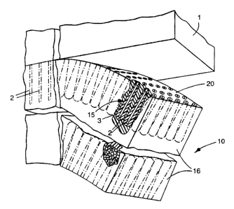
Figure 1 is a perspective view of an electrode membrane of the present
invention.
Figure la is a cross-sectional view of a nanostructured element having
a discontinuous conformal coating.
Figure 2 is a schematic of a two-electrode sensor according to the
present invention.
Figure 3 is a schematic of a three-electrode sensor according to the
present invention.
Figure 4 is a schematic of an alternative two-electrode sensor
according to the present invention.
Figure 5 is a schematic of an alternative two-electrode sensor
according to the present invention.
Figure 6 is a graphical representation of current versus time for a
sensor of the present invention.
Figure 7 is a graphical representation of EMF (mV) versus relative
humidity for a sensor of the present invention.
Description of the 'referred Embodiments)
Electrochemical devices typically comprise three primary components,
(i) a gas, liquid or solid material that is consumed in an electrochemical
(EC)
reaction, (ii) two electrically conducting catalyst electrode membranes on
which surfaces the EC reactions take place, and (iii) an electrolyte to
conduct
ionic charge and reaction products between opposing electrodes. A fourth
component (iv) may be a permeation limiting film controlling transport of the
consumed material to the catalyst surface. It is known in the art that the EC
reaction requires the presence of the three components (i-iii) to be mutually
CA 02150833 2003-04-29
60557-5004
_g_
contiguous and that optimizing the mutual conjunction of these three
components will optimize the device performance. More specifically this
invention describes a new geometric structure for the catalyst electrode
material (ii), which when incorporated intimately into a solid polymer
electrolyte (iii) or film (iv) offers a number of advantages over the prior
arts'
means for forming the electrode membrane (E/M), . including optimization of
the three component interface. Furthest aspects of this.invention teach
different ways to incorpor,~te this new Catalyst electrode fracture (ii) into
components (iii) and (iv) to form useful EC sensors, fuel cells and batteries.
The catalyst membrane structure is comprised of nanostructured
composite films (NCF), generally described elsewhere.
Contemplated to be within the scope of the present
invention are various electrochemical cell configurations using the cattily -
st
membrane structures of the present invention: The catalyst membrane
structures have been categorized to illustrate the present invention. Among
the various configurations contemplated are the following ron-limiting
examples:
(1) The membrane structure may-be-fabricated such:.that.:~.:
electrochemical cell could use at least two pieces of a nanostructured
composite film in combination with a solid polymer electrolyte film or an
electrolyte paste. Such constructions are illustrated in Figures ~ and 5.
Referring to Figures 4 and 5 an electrochemical cell (configured as a
electrochemical sensor) is schematically illustrated. A working electrode is
comprised of a first encapsulant (37) wherein a first set of nanostructured
2S elements (33) are embedded therein. A counter electrode is comprised of a
second encapsulant (38) wherein a second set of nanostructured elements {32)
are embedded therin. A conductive wire (31) is adhered to the
electrochemically active surface of the tyro electrodes. Positioned between
and in intimate contact with the electrochemically active surface is either an
electrolyte paste (40) or a solid polymer electrolyte (30): When an
electrolyte
paste (40) is used, a retaining means (39) is used to keep the paste in
position.
The figure illustrates an O-ring used as retaining means (39). The analyte
(represented
by 35) is
WO 94!15210 PCT/US93l11814
-10-
sensed through the working electrode. Typically, the first and second
encapsulants have a permeability differential, wherein the encapsulant of the
counter electrode has a lower permeability than the working electrode. .
Typically, the first and second sets of nanostructured elements are coated
with
different electrically conductive materials, although this is not required.
Other '
various coatings and enclosures can also be used.
(2) An electrochemical cell could be constructed using at least two
pieces of a nanostructured composite film wherein the nanostructured elements
are embedded in a solid polymer electrolyte. In such an instance, the film
pieces could be laminated together with the electrochemically active surface
of
the film pieces opposite each other, that is, the electrochemically active
surfaces face outward. Counter and working electrodes could be fabricated
using different solid polymers. Furthermore, the nanostructured elements can
be coated with different electrically conductive materials.
(3) An electrochemical cell could be constructed using at least two
pieces of a nanostructured composite film wherein the nanostructured elements
embedded in a solid polymer electrolyte are laminated together with the active
surface of the films facing outward and separated from each other with an
ionically conductive material, for example a solid polymer electrolyte or an
electrolyte paste. Counter and working electrodes could be fabricated using
different solid ~lymers. Furthermore, the nanostructured elements can be
coated with different electrically conductive materials.
(4) Figures 2 and 3 illustrate yet another contemplated
configuration for an electrochemical cell. Referring to Figure 2 an
electrochemical cell (configured as a electrochemical sensor) is schematically
illustrated. A working electrode is comprised of a first set of nanostructured
elements (33) embedded in a solid polymer electrolyte (30). A counter
electrode is comprised of a second set of nanostructured elements (32)
embedded in the solid polymer electrolyte (30) on the surface opposite the
first set of nanostructured elements (33). A conductive wire (31) is adhered
to
the electrochemically active surface of the two electrodes. The analyte
(represented by 35) is sensed through the working electrode. The counter
WO 94/15210 PCT/US93/118I4
~~.~0833
-11-
r ~ i
electrode is shielded from the analyte (35) by an optional impermeable layer
(34), in this illustration, a piece of tape. The first and second sets of
nanostructured elements may be coated with different electrically conductive
materials, although this is not required.
Referring to Figure 3, a three-electrode electrochemical cell is
illustrated comprising a working electrode comprised of a first set of
nanostructured elements (33) embedded in a solid polymer electrolyte (30). A
reference electrode is comprised of a second set of nanostructured elements
(32) embedded in the solid polymer electrolyte (30) on the surface opposite
the first set of nanostructured elements (33). Preferably, these two sets of
nanostructured elements are directly opposed to each other on the common
solid polymer electrolyte. A counter electrode is comprised of a third set of
nanostructured elements (36) embedded in the solid polymer electrolyte (30)
on the same surface as the reference electrode, but above or to the side of
the
second set of nanostructured elements (32). A conductive wire (31) is
adhered to the electrochemically active surface of the two electrodes. The
analyte (represented by 35) is sensed through the working electrode. The
counter electrode is shielded from the analyte (35) by an impermeable layer
(34), in this illustration, a piece of tape. The first, second and third sets
of
nanostructured elements may be coated with different electrically conductive
materials, although this is not required. Although a specific arrangement of
the 3-electrodes is illustrated, other configuration could also be used.
In the preferred embodiment of the present invention, the electrically
conductive material can be incorporated directly at the surface of an
electrolyte in an optimized geometric structural form. This geometric
structural form provides advantages over art known structures. The optimized
geometric structural form is a very dense array of acicular (large
length/width
ratio), discrete, oriented submicroscopic elements. Two-component elements,
consisting of conducting, preferably catalytic material coated around an inert
core whisker, have lengths of -1-5 micrometers (~,m), diameters -0.05-0.1
~cm, orientations substantially parallel to one another with long axes normal
to
the polymer surface, and number densities of 3 to 4 billion per cm2. Single
CA 02150833 2003-04-29
60557-5004
-12-
phase elements can, also be used, although the two-phase elements are
preferred. These single phase elements have dimensions similar to the two ,
phase elements, however, the single phase elements consist only of an
electrically conductive material.
The nanostructured elements can be randomly or uniaxially oriented. y
Perferably, the elements are uniaxially oriented because this orientation
allows
the close packing to be optimized, thereby increasing the surface area
available for reaction per unit area of membrane. The shape, orientation, size
and numbers of elements optimizes the surface area for EC reactions. Coating
the electrically conductive material around (conformally) (refer to Figure 1a)
the inert core whisker further maximizes the surface area while minimising
the amount of coating material needed. Coating this material such that it
consists of small rough particles covering the sides of the inert core whisker
(refer to Figures land 1(a)) further increases the surface area for reaction,
even over the conformally coated whiskers.
A process for making the nanostructured composite film used to
demonstrate this invention is described elsewhere. Particularly useful
nanostructured
elements comprising the nanostructured composite film are described in U.S.
Patent
No. 4,812,352.
Referring to Figure 1, nanostructured composite film (10) is
comprised of high aspect ratio whiskers (2) comprised of an organic pigment
grown such that their long axes are perpendicular to a temporary substrate
(1),
such as copper-coated polyimide. Whiskers (2) ire discrete, oriented normal
to substrate (1), predominantly noncontacting, have cross-sectional dimensions
on the order of 0.05 ~cm or.Iess, lengths of 1-2 ~m and areal number densities
of approximately 40-SO/~cm2. Whiskers (2) are then coated with a thin shell
(3) of an electrically conductive material, for example, by vacuum evaporation
or sputter deposition. Nanostructured elements (15) are then embedded into
an encapsulant (16). Typically, to construct an electrochemical cell, at,
least
one "set" of nanostructured elements are embedded in the encapsulant (16).
CA 02150833 2003-04-29
60557-5004
-13-
One set of elements are on one major surface, while the other set of elements
are embedded .on the opposite side, that is, the other major surface of the
solid .
polymer, as illustrated. Nanostructured composite film (10) (referred to as
"film") is then peeled from temporary substrate (1), cleanly carrying
nanostructured elements (15) along, embedded on tine surface of film (10),
thereby exposing the electrochemically active surface (20) of nanostructured
composite film (10). Encapsulant (16) can be (a) a solid electrolyte film, (b)
a film former or (c) a solid solution or mixture of a polymer and an
electrolyte.
Materials useful as temporary substrate (1) for the present invention
include those which maintain their integrity at the temperatures and pressures
imposed upon them during any deposition and annealing steps of subsequent
materials applied to the temp4rary substrate. The temporary substrate may be
flexible or rigid, planar or non-planar, convex, concave, aspheric or any
combination thereof.
Pieferted temporary substrate materials include organic or inorganic
materials, such as, polymers, metals; ceramics, glasses, and semiconductors.
The preferred organic substrate "is metal-coateii polyiinide film
~(commeicially
available from DuPont Corp. under the trade designation ItAPT'Oi~.
Additional examples of substrate materials appropriate for the present
invention can be found and describul in tJ~S. Patent No. 4,812,352.
Starting materials useful in preparing whiskers (2) include organic and
inorganic compounds. Whiskers (2) are essentially a non-reactive or passive
matrix for the subsequent thin metal coating and encapsulant. Several
techniques or methods are useful for producing the whisker-like configuration
of the particles. Such methods for making inorganic-, metallic-, or
semiconductor-based microstructured-layers or whisker-like structures are
described in J. Vac. Sci. Tech. A 1983, 1 (3), 1398-1402; U.S. Patent Nos.
4,969,545; 4,252,864; 4,396,643; 4,148,294; 4,155,781; and - 4,209,008.
WO 94/15210 PCT/US93/11814
~~ X0,833 _14-
Useful organic compounds include planar molecules comprising chains
or rings over which-electron density is extensively delocalized. These
organic materials generally crystallize in a herringbone configuration.
Preferred organic materials can be broadly classified as polynuclear aromatic
hydrocarbons and heterocyclic aromatic compounds. Polynuclear aromatic
hydrocarbons are described in Mornson and Boyd, Organic Chemistry, 3rd
ed., Allyn and Bacon, Inc. (Boston, 1974), Chap. 30. Heterocyclic aromatic
compounds are described in Chap. 31 of the same reference.
Preferred polynuclear aromatic hydrocarbons include, for example,
naphthalenes, phenanthrenes, perylenes, anthracenes, coronenes, and pyrenes.
A preferred polynuclear aromatic hydrocarbon is N,N'-di(3,5-xylyl)perylene-
3,4:9,10 biS(dicarboximide) (commercially available from American Hoechst
Corp. under the trade designation of "C. I. Pigment Iced 149") [hereinafter
referred to as perylene red] .
Preferred heterocyclic aromatic compounds include, for example,
phthalocyanines, porphyrins, carbazoles, purines, and pterins. More preferred
heterocyclic aromatic compounds include, for example, porphyrin, and
phthalocyanine, and their metal complexes, for example, copper
phthalocyanine (commercially available from Eastman Kodak).
The organic material used to produce whiskers may be coated onto a
temporary substrate using well-known techniques in the art for applying a
layer of an organic material onto a substrate including but not limited to
vacuum evaporation, sputter coating, chemical vapor deposition, spray
coating, Langmuir-Blodgett, or blade coating. Preferably, the organic layer is
applied by physical vacuum vapor deposition (i.e., sublimation of the organic
material under an applied vacuum). The preferred temperature of the
temporary substrate during deposition is dependent on the organic material
selected. For perylene red, a substrate temperature near room temperature
(i.e., about 25°C) is satisfactory.
In a particularly useful method for generating organic whiskers, the
thickness of the deposited organic layer will determine the major dimension of
CA 02150833 2003-04-29
60557-5004
-15-
the microstructures which form during an annealing step. Whiskers are grown
on a temporary substrate with the characteristics and process described in
U.S. Patent No. 5,039,561. An alternative process for generating the whiskers
includes
depositing a whisker generating material on a temporary substrate wherein the
whisker generating material and the temporary substrate are at an elevated
temperature. Material is then deposited until high aspect ratio randomly.
oriented whiskers are obtained. The preferred process for obtaining the
perylene red whiskeys includes depositing the whisker generating material at
or near room temperature and then elevating the substrate temperature to
anneal the whisker generating material (described in 'Example 1 hereinbelow).
In both instances, perylene red is the orgaxsic material preferred.
When the organic material is perylene red, the thickness of the layer (when
using the preferred process), prior to annealing .is in the range from about
0.05 to about 0.25 ~cm, more preferably in the range of 0,05 to 0:15 ~cm.
When the organic materials are annealed, generally uniaxially-oriented
whiskers are produced. Preferably, the whiskers are monocrystalline or
poljrcrystalline rather than amorphous: The properties; both chemical and-
physical, of the layer of whiskers are anisotropic due to the crystalline
nature
and uniform orientation of the nanostructured elements.
Typically; the orientation of the whiskers is uniformly related to the
temporary substrate surface. The whiskers are preferably substantially
uniaxially-oriented normal to the temporary substrate surface, that is,
perpetldicular to the emporary substrate surface. The major. aces of the
whiskers are generally parallel to one another. The whiskers ate typically
uniform in size and shape, and have uniform cross=sectional. dimensions along
their major axes. The 'preferred length of each whisker is in the range of 0:1
to 2.5 um, more preferably in the rmge of 0.5 to 1.5 ~cm. Thie diameter or
cross-sectional width of each whisker is preferably .~~ss than 0. r ~cm.
The v~ihiskers preferably have a high aspect ratio, (i.e., length of the
whisker to diameter or cross-sectional width of the whisker ratio is in the
range from about 3;1 to about 100:1). The major dimension of each .whisker
CA 02150833 2003-04-29
60557-5004
-16-
is directly proportional .to the thickness or amount of the initially
deposited
organic material. The areal number densities of the eonformally coated
nanostructured elements are preferably in the range of 40-50/~cm2.
The nanostructured elements, submicrometer in width and a few
micrometers .in length, are composites comprising whiskers conformally
coated with a thin electrically conductive material coating. In addition try
providing arw electrically conductive coating material, the coating material
will
generally strengthen the nanostructured.elements. 'The electrically conductive
material can be fully conformally coated over the whiskers,. producing a
generally smooth thin shell around the whiskers prefer .to Figure 1),
Alternatively, this material can be discontinuously conformally coated such
that it consists of small rough particles covering the sides of. the whiskers
(refer to Figure la) further increasing the surface area available for
reaction,
even over the: fully conformally coated whiskers. Generally, the conductive
1S coating material is selected to optimize the electrochemical reaction being
sensed. Preferably, the conductive coating material is catalytically active
and
selected from the group consisting of conducting metals, semi-metals and
seri~iconduetors: ~e~ch materials inelude~ Cr;--Co; Tr; Ni, Pd~ -Pt;- Au;-
;Ag, Cu~,
Be, Mg; Sc, Y, La, Ti, Zr, Hf, V; IVb, Ta, Mo, 'W, Mn, Tc, Re, Fe, Ru;
Os, Rh, Zn, Cd, Hg, B, Al, Ga, In, Tl, C,. 5i, Ge, Sn, Pb, As, Sb, Bi, Se;
Te and alloys thereof, such as CrCo, NiCr, Ptlr, The wall thickness of the
coating material surrounding the whiskers is in the range from about Q.S nm
to about ~0 nm. The thickness of the coating material may be such that the
resulting, nanostrstctured elements remain substantially discrete although
there
may be substantial contact between the elements.
The coating material may be deposited onto the whiskers using
conventional techniques. Preferably, the coating material is
deposited by a method that avoids the disturbance or destruction of the
whiskers by mechanical or mechanical-like forces. More preferably, the
coating.material is deposited by vacuum deposition methads, such as, vacuum
sublimation, sputtering, vapor transport, and chemical vapor deposition.
WO 94/15210 ~ ~ ~ ~ PCT/US93/11814
-17-
Essentially, the nanostructured elements provide a three dimensionally
distributed enhanced surface area which is potentially all available for
catalytic
reaction compared to the planar or two dimensionally distributed area of art
known grid surfaces contacting an SPE.
The encapsulant is such that it can be applied to the exposed surface of
the nanostructured elements in a liquid or liquid-like state, which can then
be
solidified or polymerized. The encapsulant may be in a vapor or vapor-like
state that can be applied to the exposed surface of the nanostructured
elements. Alternatively, the encapsulant is a solid or solid-like material,
preferably powder or powder-like, which can be applied to the exposed
surface of the nanostructured layer, transformed (e.g., by heating) to a
liquid
or liquid-like state (without adversely affecting the nanostructured layer
composite), and then resolidified.
Organic encapsulants include thermoplastic polymers and co-polymers
and include, for example, polymers derived from olefins and other vinyl
monomers, condensation polymers, such as polyesters, polyimides,
polyamides, polyethers, polyurethanes, polyureas, and natural polymers and
their derivatives such as, cellulose, cellulose nitrate, gelatins, proteins,
and
natural and synthetic rubbers. Inorganic encapsulants that would be suitable,
include for example, gels, sols, semiconductors, or metal oxides applied by,
for example, vacuum processes. Preferably, the thickness of the encapsulant
is in the range from about 1 ~cm to about 1 cm, and more preferably in the
range from about 25 ~cm to about 2 mm.
The encapsulant may be applied to the nanostructured elements by
means appropriate for the particular encapsulant. For example, an
encapsulant in a liquid or liquid-like state may be applied to the exposed
surface of the nanostructured elements by dip coating, vapor condensation,
spray coating, roll coating, knife coating, or blade coating or any other art
known coating method. An encapsulant may be applied in a vapor or vapor-
like state by using conventional vapor deposition techniques including, for
example, vacuum vapor deposition, chemical vapor deposition, or plasma
vapor deposition.
WO 94/15210 PCT/US93/11814
_18-
An encapsulant that is,solid or solid-like may be applied to the exposed
surface of the nanostructured elements when liquified by application of a
sufficient amount of energy, for example, by conduction or radiation heating
to transform the solid or solid-like material to a liquid or liquid-like
material,
and then solidifying the liquid or liquid-like material. Alternatively, the
nanostructured elements may be embedded into a solid or solid-like
encapsulant by hot-roll calendering, that is using heat and pressure with a
force sufficient to embed the nanostructured elements into the solid
encapsulant, but without damaging the nanostructured elements.
The applied encapsulant, if liquid or in a liquid-like state, may be
solidified by means appropriate to the particular material used. Such
solidification means include, for example, curing or polymerizing techniques
known in the art, including, for example, radiation, free radical, anionic,
cationic, or step growth processes, and solvent evaporation, or combinations
thereof. Other solidification means include, for example, freezing and
gelling.
After the polymer is cured, the resulting nanostructured composite film
of the present invention comprising nanostructured elements intimately
encapsulated in an encapsulant is delaminated from the temporary substrate at
the substrate:nanostructured element layer interface by mechanical means such
as, for example, pulling the film from the temporary substrate, pulling the
temporary substrate from the film, or both. In some instances, the film may
self delaminate during solidification of the encapsulant. Removal of the
temporary substrate exposures the active surface of the nanostructured
composite film.
Alternatively, the encapsulant can be a solid polymeric electrolyte.
One example of such a solid polymer electrolyte is Nafion''" 117, a
perfluorinated sulfonate ion exchange polymer commercially available in sheet
form 0.028 cm thick or as a dilute solution, which can then be coated onto the
nanostructured elements and then solidifed using art known techniques.
Alternatively, an electrolyte can be mixed with a curable encapsulant and
cured or the electrolyte can be incubated or allowed to permeate into a cured
CA 02150833 2003-04-29
60557-5004
-19-
encapsulant. In contrast to the Nafion''" film, in these alternative forms the
ionic element in the encapsulant is merely dissolved in the encapsulant, as
opposed to being an integral part of the encapsulant's chemical structure.
Alternatively, a solventless process for embedding the.nanostructured
elements into a solid encapsulant can be used. Although applicable in concept
to any nanostructured surface phase, that is, one comprising nanostructured
elements of various material compositipns, shapes, orientations, .and packing
densities the description of the process refers to the electrode membranes.
The nanostructured elements are hot pressed into the surface of the
solid encapsulant by a calendering process, using controlled heat and
pressure.
For example, the nanostructured elements are brought into contact with the
solid encapsulant at the nip part of a pair of heated rollers. The temporary
substrate (from the nanostructured elements) is then stripped away, leaving
the
nanostructured elements penetrating the solid encapsulant that completely
preserves their orientation and at~eal number density.
Placement of the nanostructured elements wholly within an
electrolyte-containing encapsulant maximizes the catalyst
electrolyte~interface,
and protects the~eIeinents from darriageFurtheivmore, having the elements
coincident with the electrolyte-containing encapsulant surface optimizes the
accessiblity of the analyte (gas or liquid consumed) to the
catalystlelectrolyte
three component interface. The discreteness of the nanostructured elements
allows the surface electrode layer to remain permeable to the arialyte, while
the close pacldhg of the elements assures the nanostructured composite films
(NCF) remain electrically conducting as described elsewhere.
Alternative embodiments of this invention utilise the NCFs formed
with the nanostructured elements encapsulated in a nanelectrolyte containing
encapsulant, for use with liquid, paste (non-solid); or solid electrolytes.
1,n
this configuration, the nanostructured elements provide surface conductivity
to
the polymer and a electrochemically active surface in contact with the non
solia electrolytes while the encapsulant may function also as a diffusion
limiting membrane (see Figures 4 and 5).
CA 02150833 2003-04-29
60557-5004
-20-
This invention is useful in electrochemical devices, such as gas, vapor
and liquid sensors, fuel cells and batteries formed using the optimized
electrode membrane construction.
Objects and advantages of this invention are further illustrated by the
following examples, but the particular materials and amounts thereof recited
in
these examples, as well as other conditions and details, should not be
construed to unduly limit this invention. All materials are commercially
available or 'known to those skilled in the art unless otherwise stated or
apparent.
1o Examples
Preparation of the Whis ers
In the following examples, nanostnuctured elements according to the
present invention were prepared using processes described in U.S. Patent Nos.
4,812,352 and 5,039,561.
Briefly, N,N'-di(3,5-xylyl)perylene-3,4:9,10 bis(dicarboximide),
(hereinafter referred to.as PR 149), was vacuum vapor deposited onto a
flexibie polyimide web, near room temperature, to a thickness on the order of
0.1 to 0.15 ~cm. Thereafter, the substrate and PR 149 coating were annealed
in a vacuum sufficient to cause the initially .uniform pigment film to convert
to
a highly nanastructured film, After:annealing, the whiskers. were discrete,
uniformly oriented single crystals; 1 to .2 p,m tall, with high aspect ratios
(length to width), extremely.Iarge areal number densities (4p-SO/~,m2), and
whisker to whisker spacings on the order of 0.05 ~sm. The resulting
geometric surface area was increased by a factor of 10 to 15. The .whiskers
were then coated with a conducting material. .The coated whiskers
(nanostructured elements) were then embedded into the surface of a polymer
to form a nanostructured composite film.
In the following examples, nanostructured,composite films are
demonstrated in two.alternative embodiments, using two modes of .operation,
W094/15210 ~~~0~~3 .
PCT/US93/11814
-21-
and in both two and three electrode configurations (see Figures 2-5).
Electrodes of the nanostructured composite films can take the form of
electrode membranes wherein the conducting coated whiskers are embedded in
a permeable polymer membrane which is then placed in contact with the
electrolyte (Examples 6-24), or the nanostructured elements may be placed
directly within the surface of a solid polymer electrolyte (Examples 1-5 and
25). The sensors may be operated in both a potentiometric (open circuit EMF
measurement) or amperometric mode. The amperometric mode can be of
either a two or three electrode (potentiostat controlled) configuration.
.example 1
This first example demonstrates the nanostructured composite films as
high surface area electrodes embedded within the near surface region of a
solid polymer electrolyte.
The nanostructured elements were first constructed as described above
producing discrete, oriented whiskers, 1-2 ~cm in length on a Cu-coated
polyimide temporary substrate. The whiskers were then coated with a mass
equivalent thickness of 175 nm Pd by vacuum evaporation to produce
nanostructured elements. A curable solid polymer electrolyte formulation
consisting of 0.45 gram lithium perchlorate (LiC104) in 1 ml tetrahydrofuran
(THF), 0.75 ml catalyst solution consisting of 25 ~,1 dibutyl tin dilaurate in
10
ml THF, 1.5 ml 600 molecular weight polyethylene glycol) and 1.5 ml
Desmodur'"' N100 (Farbenfabriken Bayer AG) multifunctional isocyanate.
The sensor was made as follows: Approximately 0.1 ml of the curable
solid polymer electrolyte solution was placed between two 10 mm diameter
discs cut from the temporary substrate supporting the nanostructured elements.
The sample was cured at approximately 40°C for a period of about
one hour.
The temporary substrate of the nanostructured elements was then peeled away
from the cured solid polymer electrolyte leaving the fresh, Pd-coated
nanostructured electrodes embedded in the surface (catalytically active
surface)
of each side of the solid electrolyte disc (see Figure 2). Electrical contact
to
WO 94/15210 ~ PCT/US93/11814
-22-
both sides of the nanostructured electrode membrane was made using 0.3 mm
diameter copper wire adhered to the electrode membrane with a trace amount
of conducting silver paint (GC Electronics, Rockford, IL). One side of the
membrane (counter electrode) was then isolated by covering the entire surface
with a 10 mm diameter piece of vinyl plastic electrical tape (commercially
available from 3M).
The sensor was then exposed to 10 ppm hydrogen sulfide (H2S) at
approximately 10% relative humidity. The 10 ppm HZS stream was generated
by the addition of 0.2 liters per minute from a compressed air tank containing
500 ppm HZS (Oxygen Services Company, St. Paul, MN) to 10 liters per
minute (llmin.) air having 10% relative humidity. Exposure to the gas caused
the sensor to generate an amperometric current signal. This resulting current
signal was monitored with a Keithley 197A electrometer. A rapid response
time of less than one minute to reach a steady state current of 0.1 ~cA with a
signal to noise ratio of approximately 100 was observed. This corresponds to
a sensitivity on a unit concentration, unit area basis of 0.013 ~A ppm'' cm-2.
Upon removal of the hydrogen sulfide stream, the sensor showed a rapid
( < 1 minute) reversible recovery to the original baseline (as measured with
10% relative humidity air).
Examples 2-5
Examples 2-4 describe a 3-electrode sensor comprising a working,
counter and reference electrode membranes fabricated from nanostructured
elements pressed directly into a solid polymer electrolyte. Example 5
describes a 2-electrode sensor comprising working and counter electrode
membranes fabricated from nanostructured elements pressed directly into a
solid polymer electrolyte. These examples show that compared to art known ,
sensors made with metal mesh-powders/Nafion'''" or metal grid/Nafion''" film
electrodes, the nanostructured electrode membranes/Nafion'"' film sensors
show 50 to 100 times the response to N02 and H2S in units of microamps per
ppm (p,A/ppm) of gas per unit planar area of working electrode.
WO 94/15210 PCT/US93/11814
-23-
The nanostructured composite film (NCF) based electrochemical sensor
electrodes show measured gain factors of 50 to 100. They consist of oriented,
metal coated organic whiskers, pressed into the surface of Nafion''" film, or
otherwise encapsulated in the surface of an SPE. The particles are - 2 ~.m
long, - 0.05 ~,m in diameter, and have packing densities -- 3-4 x 10⁹/cm2,
which with relatively small amounts of metal coating thicknesses makes the
composite surface conductive. The BET Nz surface area enhancement factor
for these whiskers with Pt-sputtered onto them to form "nanoscopically"
"lumpy" conformal coatings have been measured to be --- 3000. Part of this
factor appears to be due to the 10-15 fold increase in surface area due simply
to the geometric surface area increase, implying that the surface area
increase
due to the nanoscopic structure of the Pt on the whiskers is approximately
200. In contrast, a surface roughness factor of y -r 1.4 is a given
characteristic for bulk-like "bright" gold in Opekar (1992).
xam 1 2
The nanostructured composite film having discrete, oriented whiskers
on a Cu-coated polyimide temporary substrate was grown as described above.
The working electrode membrane was constructed by coating <_ 1 ~,m tall
whiskers with a mass equivalent thickness of 200 nm of Au by vacuum
evaporation to produce catalytically coated whiskers. The counter and
reference electrode membranes were constructed from nanostructured elements
of 200 nm Pt vacuum evaporated onto whiskers 1-2 ,um tall. Nafion~' 117
film (commercially available from Du~nt) was the solid polymer electrolyte
(SPE) in this case.
The 3-electrode sensor was constructed from two 10 mm discs cut
from the temporary substrate supporting the nanostructured elements (Au-
coated and Pt-coated). The elements were pressed into a 1.5 cm by 3.5 cm
piece of 0.028 cm thick Nafion'"' 117 film using a laboratory press (Fred S.
Carver Inc., Wabash, III at a temperature of 149°C and a force of
8,900
Newtons (1 ton) for a period of about 3 minutes. The configuration of the
WO 94/15210 ~ ~ a 0 8 3 3 PCT/LJS93/11814
-24-
sensor (see Figure 3) was such that the working electrode (Au-coated
elements) and the counter and reference electrodes (Pt-coated elements) were
on opposing sides of the Nafion"' 117 film, with the reference electrode
directly behind the working electrode and the counter electrode to the side of
the reference electrode. Electrical contact to the electrodes was made using
0.3 mm diameter Cu wire. The entire structure was encapsulated with vinyl
plastic electrical tape. A 6 mm diameter opening was left in front of the
working electrode, allowing exposure to the gas analyte.
A PAR model 273A potentiostat (EG & G Princeton Applied Research,
Princeton, N.J.) was used to measure the resulting current on exposure to the
gas analyte while maintaining a constant potential bias between the working
and reference electrodes. In this example, the sensor was exposed to 200 ppm
N02 at 78 % relative humidity while maintaining a bias of -0.3 V between the
working and reference electrode. The NOZ stream was generated by adding 2
ml/min of pure NO~ gas (Matheson, East Rutherford, N. J.) to 10 1/min air at
78! relative humidity and 23°C. The sensor response is shown in Figure
6.
The sensor gave a large, rapid response reaching a steady state current of
0.75
mA in approximately 1 minute. Upon removal of the N02, the sensor quickly
returned to the baseline value with a recovery time of less than 1 minute. The
magnitude of this signal corresponds to a sensitivity of 13.4 ~cA pprri 1
cm'2.
This can be compared with a literature value (Opekar 1992) of 0.26 ~cA ppni 1
cm'2 for a Au square grid pressed into the Nafion"' 117 film as a working
electrode under identical conditions of relative humidity and bias. By this
example, use of the nanostructured electrode membrane of the present
invention has improved the sensitivity by a factor of 51.5, or over 5000% .
Example ,
In this example, a bias of +0.3 V was applied to the working electrode
with respect to the reference, and the sample exposed to 200 ppm NO2, all
other conditions being equal to those in Example 2. In this case, a rapid,
reversible response was again observed with a steady state signal of 0.14 mA.
WO 94/15210 PCT/US93/11814
-25-
This corresponds to a sensitivity of 2.5 ~cA pprri 1 cm Z. This can be
directly
compared with a literature value of 0.024 ~,A ppm-1 cm-Z (Maclay et al., 1988)
using a standard Au meshlAu powder working electrode under equivalent
conditions. A factor of 104, or over 10,000%, improvement in sensitivity is
obtained over the art known pressed electrode system.
Exaxn~le 4
In this example, the same sensor as in Examples 2 and 3 was exposed
to a 10 ppm H2S gas stream while maintaining a bias of +0.3 V between the
working and reference electrode. The 10 ppm HAS gas stream was generated
by mixing 0.2 1/min of a 500 ppm HZS compressed air cylinder (Oxygen
Services) with 101/min air at 78 % relative humidity and 23 ° C. A
rapid,
reversible response was observed with a steady state current of 79 ~,A. This
corresponds to a sensitivity of 28 ~cA ppm'I cm 2; a factor of 87.5 over a
literature value (Maclay 1988) of 0.32 ~,A pprri 1 cm z for a standard Au
mesh/Au powder electrode under equivalent conditions.
Exam In a 5
Example 5 shows a nanostructured element/Nafion~' 117 film
construction that can be used as a ~tentiometric two electrode humidity
sensor, particularly in inert gases, with both electrodes exposed to the same
ambient.
A 2.5 cm square piece of Nafion~' 117 membrane sheet, as used in
Example 2, was formed into a two electrode sensor by hot platen pressing Au
coated whiskers into one side of the sheet and NiCr-coated whiskers into the
opposite side. Two samples of nanostructured whisker (1 -1.5 ~cm tall)
samples were prepared as described above, on a Cu-coated polyimide
temporary substrate, and overcoated with sputter-deposited Au in one instance
and sputter-deposited NiCr in the second. The planar equivalent thickness of
the Au coating was on the order of 200 nm and that of the NiCr coating
nominally 220 nm. The Au-coated nanostructured elements were placed with
WO 94/15210 PCT/US93/11814
-26-
the elements against one side of the NafionT" 117 film piece. Both were
sandwiched between larger sheets of 0.0048 cm thick polyimide (a processing
aid used to protect the platens). The sandwich construction was pressed ,
between the platens of the Carver laboratory bench press for 15 seconds, with
the platens maintained at a temperature of 138°C and a total applied
force of
(two tons) 17,800 Newtons.
After pressing, the temporary substrate peeled cleanly away from the
Nafion''" ,117 film leaving the Au-coated whiskers embedded in the latter.
This procedure was repeated, pressing for 20 seconds, to embed the NiCr-
coated whiskers into the other side of the Nafion"' 117 film piece. A 3 cm x
1 cm strip was cut from the piece for testing. Electrical contact was made to
each side of the strip with clip leads with only one jaw touching each
respective side. An electromotive force (EMF) potential existed between the
two leads with the sample in open air, the Au-coated side was positive with
respect to the NiCr-coated side. The sample was then placed in a sealed
container, with humidified N2 flowing at 5 liters/min. The EMF was
monitored with a chart recorder having an input impedance of 2.5 Mohm, as a
function of the relative humidity (%RH) in the sealed container, measured
with a General Eastern humidistat. The EMF was observed to vary nearly
linearly between zero and 0.37 volts with % RH between 10 % to 95 % , as
shown in Figure 7.
Examples 6 - 24
Examples 6-24 describe an alternative construction wherein the
nanostructured composite electrode is embedded in the surface of a permeable
polymer film for the working electrode and a low ~rmeability polymer film
for the counter electrode (see Figure 4). The sensors were produced by
r
sandwiching an electrolyte paste between a working and counter electrode.
The electrolyte paste was adjacent to the active surfaces of each
nanostructured composite film.
r
WO 94/15210 ~ ~ '~ ~ ~ ~ ~ PCT//11S93/11814
-27-
Example 6 (Electrol,~A~l
The membrane electrodes for this configuration were constructed by
casting a 5 wt % solution of encapsulating polymer onto nanostructured
elements consisting of a 175 nm thick Pd coating on PR 149 whiskers grown
on the Cu-coated polyimide temporary substrate as described above. The
encapsulating polymer for the working electrode was poly(trimethly silyl
propyne) (PT MSP) (Huts Petrarch). The encapsulating polymer for the
counter electrode was poly(ethyl methacrylate), a polymer with a lower
permeability than PT MSP. The volume of encapsulating polymer solution
provided a dried film approximately 0.1 mm thick. After evaporation of the
solvent, the nanostructured composite film was peeled away from the
temporary substrate exposing the Pd-coated nanostructured elements at the
surface of the nanostructured composite film. An electrolyte paste was
prepared by adding 0.5 ml concentrated HZS04 to 1 gram 100,000 molecular
weight (MVO poly(ethylene oxide).
The sensor was then assembled in the following manner (see Figure 4):
Electrical contact was made to 10 mm diameter discs of the working and
counter electrodes using 0.3 mm diameter copper wire adhered to the surface
of the electrodes with a trace amount of silver paint (GC Electronics). A
small, 6 mm inner diameter O-ring was filled with the electrolyte paste, and
the two electrodes were then glued (3M CA-4 cyano acrylate adhesive)
(exposure surfaces inward) to the perimeter of the O-ring leaving the
nanostructured surface composite film to form an initimate contact with the
electrolyte paste.
To measure the sensor response, a 100 Ktl load resistor was connected
between the sensor leads, and the voltage across the load resistor, resulting
from the current signal, was monitored with a Keithley 197A electrometer.
The sample was then exposed to 10 ppm H2S in 10 % relative humidity air at
23°C. The H2S stream was generated by mixing 0.2 1/min of a preformed
500 ppm HZS/compressed air tank (Oxygen Services) to 10 1/min of 10%
WO 94/15210 ~ '" PCT/CTS93/11814
~.~~~~3
-28-
relative humidity air. A rapid, reversible response to the H2S was observed
with a steady state voltage corresponding to 0.032 mV.
Table 1
Electrolyte Paste
0.25 gram LiC104 dissolved in 0.25 ml HPLC
grade water
B added to 1 gram 100,000 MW polyethylene oxide)
0.5 ml 85 % H3P04 added to 1 gram 100,000
MW
C polyethylene oxide)
0.25 gram C6HSS03H dissolved in 0.25 ml HPLC
grade
D water added to 1 gram 100,000 MW polyethylene
oxide)
0.26 gram NH4Cl dissolved in 0.5 ml HPLC
grade water
E added to 0.25 gram 100,000 MW polyethylene
oxide)
Examples 7-24
The electrodes and sensor construction for these examples were
prepared as described in Example 6. The various electrolyte pastes used in
the sensor constructions were as described above in Table 1. The sensors
were evaluated with various gases. All the gases used were diluted to 10 ppm
in air at 10 % relative humidity, 23 ° C and a flow rate of 10 1/min.
The
results are summarized below in Table 2.
WO 94/15210 ~" PCT/US93/11814
-29-
Table 2
Example Electrolyte Gas Signal
(m~
7 B N02 0.2
8 B HZS 0.005
9 B S02 0.02
B NH4 0.003
11 B Cl2 0.048
12 B HCl 0.086
13 B CO 0.004
10 14 C HZS 0.086
C C12 0.008
16 C HCl 0.008
17 D HzS 0.012
18 ~ D CO 0.004
15 19 D NOZ 0.003
E H2S 0.04
21 E SOZ 0.1
22 E NH4 0.01
23 E CO 0.002
20 24 E C12 0.004
Example 25
In this example, a sensor was constructed by incubating a cured
polymer/electrode sample in a solution of electrolyte and subsequent removal
of the solvent. The nanostructured elements were the same as those described
in Example 1.
The curable polymer formulation was 2 grams of 2000 molecular
weight poly(tetrahydrofuran) dissolved in 2 ml THF, 10 ~cl dibutyl tin laurate
catalyst and 0.5 ml Desmadur'''" N100 brand isocyanate. Approximately 0.1
CA 02150833 2003-04-29
60557-5004
ml of this solution was cured between two 10 mm diameter
discs of the temporary substrate supporting the
nanostructured elements for approximately one hour at 23°C.
Upon removal of the temporary substrate, the dried and cured
5 sample having the nanostructured elements on each face of
the disc was incubated in a 5 wt% solution and allowed to
dry. Electrical contact to the two electrodes was made
using 0.3 mm diameter Cu wire, and the sensor was
encapsulated with vinyl electrical tape leaving a 6 mm
10 diameter hole in the electrical tape for exposure of the
working electrode. The sample was exposed to 10 liters per
minutes of 10 ppm HzS in air at 57% relative humidity and
23°C producing a rapid (<1 minute), reversible response of
o.1 uA.
15 Alternative Embodiments of the Present Invention
A nanostructured composite film comprising:
(a) a plurality of nanostructured elements,
wherein the nanostructured elements are acicular, discrete,
oriented, sub-microscopic, two-component structures
20 comprised of whiskers coated with a conductive material; and
(b) an encapsulant layer, comprising an
encapsulant wherein one end of each nanostructured element
is embedded within the encapsulant layer and the other end
of each nanostructed element is coincident with a first
25 surface of the encapsulant layer, such that the first
surface is a conductive surface.
The nanostructured composite film as previously
described, wherein the whiskers are uniaxially oriented
normal to the film surface.
CA 02150833 2003-04-29
60557-5004
31
The nanostructured composite film as previously
described, wherein the conductive material is selected from
the group consisting of conducting metals, semi-metals and
semiconductors.
The nanostructured composite film as previously
described, wherein the encapsulant is a solid electrolyte.
The nanostructured composite film according to
claim 14, wherein the encapsulant is a perfluorinated
sulfonate ion exchange polymer.
The nanostructured composite film as previously
described, wherein an electrolyte is dissolved in the
encapsulant.
A nanostructured electrode membrane comprising at
least one set of nanostructured elements, wherein one end of
each nanostructured element is embedded in a portion of an
encapsulating solid electrolyte and the other end of each
nanostructured element is coincident with a first surface of
the encapsulating solid electrolyte.
The nanostructured electrode membrane as
previously described, further comprising a second set of
nanostructured elements en~edded in the encapsulating solid
electrolyte polymer, such that the first set and second set
of nanostructured elements are on opposite surfaces of the
encapsulating solid electrolyte polymer.
The nanostructured electrode membrane as
previously described, wherein the first set of
nanostructured elements are coated with a conductive
material different from the conductive material of the
second set of nanostructured elements.
CA 02150833 2003-04-29
60557-5004
32
The nanostructured composite film as previously
described, further comprising a plurality of nanostructured
elements embedded in a surface opposite the first surface,
such that both the first and the opposite surfaces of the
encapsulant layer are conductive surfaces.
The nanostructured electrode membrane as
previously described, further comprising a second set of
nanostructured elements embedded in a portion of a surface
opposite the first surface, such that both the first and the
opposite surfaces of the encapsulating solid electrolyte are
conductive surfaces.
The nanostructured electrode membrane as
previously described, further comprising a third set of
nanostructured elements embedded in either the first surface
or the opposite surface of the encapsulating solid
electrolyte, such that there are three conductive areas,
with two conductive areas on the first surface and one
conductive area on the opposite surface of the encapsulating
solid electrolyte.
Various modifications and alterations of this
invention will become apparent to those skilled in the art
without departing from the scope and principles of this
invention, and it should be understood that this invention
is not to be unduly limited to the illustrative embodiments
set forth hereinabove.