Note: Descriptions are shown in the official language in which they were submitted.
wo 94/14174 2 1 ~ O 9 ~ 3 K~/US93/1191~
FLEXIBEETRANSFQRMEl~APPAiR~TllS PARTICULARl,Y
ADAPT~n FOR ~ H VQLTAGEOPERATION
The subject matter of this invention is in part contained in a Disclosure
Document No, 317330 filed with the United SLates Patent Office on September 21,
1992.
S TP~hni~ ield of the I
This invention relates to a lldll~ru~ apparaLus in general and more
particularly to a flexible Lld"~ru-l~ apparatus which is particularly adapted for use
as a fiyback Ll~ ru~ l as those employed in television seLs.
B~ d Art
Tl.~ rull~ are utilized in a wide variety of,~ A flyback
ll~"~ro""~, is a device which is used to generate a high voltage as is employed in TV
receivers and o~rillocropP~ for biasing Lhe caLhode ray tube or CRT. These
Lldllarull~lcl~ produce relatively large voltages at relativeiy small currents. The ability
lO produce a large voltage resides in Lhe number of tums that are associated with the
secondary winding, as compared to Lhe number of Lums associated with Lhe primarywinding. As is well known, the tums of the secondary, as compared to the turns of
Lhe primar~, determine Lhe volLage step up of the L,d"~r.,l,.l.l. Such flybaci
transfommers can operate as tuned L.~nsru""~l~ which consist of a primary winding
and a number of secondary windings which are runed or resonated. These secondarywindings are wound on the same bobbin and each adjacent secondary windings are
connected in series through a diode. This type of flyback Lldll~ru.lll.l is referred to
as a tuning flyback transfommer where a horizontal output pulse or flyback pulse is
applied as an input pulse to the tuned primary winding.
Anodd order higher ilammonic waveofa r",.,~- ", .IIAI frequency applied
to the primary winding, such as for example, the third hammonic is Luned and provided
at the secondary winding, based on the disLributed capacity of the secondary windin~
which is small. In this maMer the Lldll~ru~ .. provides a high vol e at the output
WO 94/14174 PCT/U593/11919
2150953
of the secondary winding. As indicated, such Lldllarul~ a are well known. Many
such lldllafullll~ls utilize a toroid or core of a donut shape fabricated from a magnetic
material of a given y~ biliLy, which core can be wound with wire. In the ideal
core, the winding represents a uniform current sheath circulating about the core in
appropriate planes. In this ideal case, the magnetic field is entirely conf~ned within
the core, the magnetic field lines are concentric circles and each links with the entire
current volume. Such a uniform distributed current flow around the core results in
a leakage free configuration. However, this is not the case in practical applications.
Other Lldllarullllcla utili2e cores which are square shaped having
multiple le~s. Both the primary and secondary windings rest on one leg. Thus thecurrent distribution around the core is by no means uniform. Ieading to a cenainamount of leakage flux. Such ~:u~ ,.lLiolldl ildllarUllllC. features typically provide
leakage flux in the order of 6%, a frequency response in the ranges between 30 Hz
and 28 kH2. The efficiency of such Lld.larul-ll.ls is on the order of 85% with the
voltage regulation being about 1.5 - 2 megohms. The si2e, both of the toroid and in
these E-shaped Lldllarullll~la is bulky and the material is not fully or optimumly
utili2ed. The winding employs solid round wires and coupling to the core is not really
ideal, leading to local leakage.
As the prior an can ascenain, when such Lldllarulll.~,.a are used as
flyback L.dllarull.l.. a they can provide relatively high voltages ranging from 7 - 28 KV
and higher. In any event, the high voltage regulation is poor. If the high voltage
regulation is poor, the ~yludu~,d picture of a TV receiver can suffer deterioration.
The prior art was aware of this, and provided certain solutions involving using multi-
layer winding flyback LldllarOllll~la which were designed to operate to provide more
stable high voltage regulation. The multi-layer winding flyback Lldllarullll~l has been
described in many U.S. patents. The problems with these L~dl~arul lll.la relate to shon
circuit operation where if a short circuit occurs on a secondary winding, or if discharge
is caused within the picture tube, the diodes associated with such transformers are
subjec=d to high reverse voltages which can operate to destroy these diodes.
wo 94114174 21~ ~ 9 ~ 3 PCT/US93111919
The prior an is replete with a number of patents which describe various
flyback lldll~rul..~ . See U.S. Patent No. 3,866,0~6entitled "Flyback Transforrner
Apparatus" issued on l~ebruary 11, 1975 to Miyoshi, et al. This describes a flyback
L-d-~rull~ where the primary winding is inductively coupled with the high voltage
side winding portion of the first secondary winding. The transformer provides anoutput impedance which is reduced and a focusing voltage which is relatively
regulaLed.
U.S. Patent No. 3,904,928 entitled "Flyback T.d.~ro.. " issued on
September 9, 1975 to Sawada, et al. This patent describes a flyback transformer
which utilizes a magnetic core with secondary windings wound around the core anda primary winding. In this transformer the secondary winding is divided into a
plurality of winding units which are alternately connected with the same number of
rectifying elements such as diodes in series. The structure is such that a relatively
compact device can be :Irrr~mmr~ tp~l,
U.S.Patent No. 4,204 7t~ nti~1~ d "FlybackTransforrner" issued on May
20,1983 to Onoue. This patent describes a flyback lldll~rull~ having a plurality of
secondary windings wound about a magnetic core. The secondary windings are
divided into a plurality of coil units and are alternately connected in series with a
plurality of rectifyin~ diodes. The coil urlits are wound around individual layer
bobbins where the bobbins are assembled in layers and fitted alternately with the
outermost bobbin being mounted with a support in which a plurality of diodes arefixed. The strucLure purpons to be relatively compact.
U.S. Patent No. 4,229,786entitled "Flyback Transformer With A Low
Ringing Ratio" issued on October 21,1980 to Mitani, et al. This patent describes a
flyback transformer having a teniary winding for obLaining a secondary power source
which is wound in a position where the coupling with the primary winding is weak and
where the winding interlinks the leakage flux of Lhe secondary winding with the
primary winding. The output of the tertiary winding is rectified during the horizonLal
WO 94114174 PCT~lS93/11919
2~50953 4
scanning period of a television receiver. In this maMer the wave crest of the ringing
is made smaller rer~ardless of the pulse which is applied to the secondary winding.
U.S. Patent No. 4,266,269entitled "Flyback~r.d.,arulll.., " issued on May
5, 1981 to Toba. This describes a multilayer flyback ~.~ulsfu.ll..,l which has flve
cylindrical bobbins which are concentrically arranged. A magnetic core is inserted in
the first or innermost bobbin and a primary winding is wound in layers on the outer
periphery of the bobbin. Diodes are connected between the secondary windings anda capacitor is formed between the cathode of the diode and the anode of another
diode. In this manner the l,d. arollll,l is capable of providing high voltage operation
in a relatively compact design.
U.S. Patent No. 4,639,706 entitled "Flyback Tlal"fu.~ " issued on
Januar,v 27,1986 to Shimizua. This patent describes a flyback ~IdllarOIIII~I where a
tertiary coil is wound on an auxiliary bobbin which is separately provided. The bobbin
is inserted on a low tension coil bobbin for the primary coil which serves to insulate
the tertiary coil from the primary coil.
U.S. Patent No. 5,122,947 entitled "Flyback Transformer Having Coil
Al~ Capable of Reducing Leakage of Magnetic Flux" issued on June 16,
1992 to Hishiki. This patent describes a flyback ll~llsf~n..l~l which uses a magnetic
core assembly formed by joining a pair of first and second U-shaped core halves each
having two leg portions with end surfaces respectively joined in a mutually abutting
~o,.r.~ There are gap spacers interposed between the first and second core
parts and a coil is wound about the core parts. The resulting ~lallar~,.",~l has an
output winding, which is a secondary, which can be divided into at least two windings
to provide separate flux paths.
As one can ascertain, apart from the above-noted patents there exists
many more pâtents which involve various Lldllaro"-l~ r~ "~ and which
attempt to reduce the size of the lldllarUIlll~,l while making the ~ r~,l".~la more
efficieM. For examples of such prior art, reference is made to U.S. Patent No.
4,103,267issued on July 25, 1978 to Olschewski entitled "Hybrid Transformer Device" .
wo 94114174 21~ 0 9 ~ 3 PCT/US93111919
This patent describes a Lla--~ru,--,~l mounted on a ceramic substrate having a plurality
of planar conductors formed on a surface of the substrate. The conductors extendradially from an imaginary point on the substrate. A layer of dielectrjc material is
formed over the major portions of each of the conductors to form a ring of dielectric
S material to which is ferrite toroidal core is secured. The core is precoated with an
il~sulating material prior to adhesively being secured to the dielectric ring. A plurality
of wire conductors are wire bonded al each end to the exposed ends of the metal
conductors on a substrate to form a printed circuit l,d.,~ro,ll,~,
U.S. Patent 4,524,342issued on June 18, 1985 to Joseph Mas and is
entitled "Toroidal Core El~l,llullla~ Device". This patent describes an
Cl~.,llUIll..~ iC device which can include a l,a.,~ru""~. and has a ma~netic core and
a segmented electrical winding. The core has an enclosed trunk deftning a central
opening. At least three coil sections of the electrical winding ~ncircle the trunk and
are ~ uulllr~ idlly spaced about the periphery of the core.
U.S.Patent 4,724,603issued on February 16,1988 to Blanpain et al. and
is entitled ~Process for Producing a Toroidal Winding of Small Dimensions and
Optimum Geometry". This patent describes an process to produce a small toroid.
Windings having turns which are radial with respect to a cylinder are employed. The
cyiinder is provided with slots arranged along the axes of an internal and external
cylinder. Hairpin shaped conductive wires are introduced into these slots and welded
to one another.
As one can also ascertain, there are many other patents which
essentially describe improved magnetic circuits used for small compact ~la.l~ru-as well as for flyback transformers.
The present invention describes a fiexible lldl-~r~"",.l which operates
without cu.,~ al wires and is capable of improved operation in providing a
reduced leaicage flux, a higher frequency response~ improved efficiency, improved
voltage regulation while providing a compact and efficient design.
WO 94/14174 ~ pcTn~ss3lll9l9
2~09~3 6
Disclosure of the Invention
A ~ fu~l.l secondary winding comprising a flexible laminated
member, comprising a first planar sheet member having a flrst plurality of parallel
conductive lines on a surface thereof, a second planar sheet member having a second
plurality of parallel conductive lines of a surface thereof, a central planar sheet
member fabricated from a rn~vnPti7:1hle material interposed between said first and
second planar members and means for coMecting ends of said first and second
parallel lines to one another to form a coiled pattern directed about said central
member to enable any current flowing in said coiled pattern to magnetize said central
planar sheet according to said current flow.
Urief Description of the Drawin~s
For a better ",.~ of the present invention, reference is made
to the following description of an exemplary ....t,.~.l;,....,l thereof, considered in
~,-; with the accu~ drawings, in which:
FIG. I is a perspective plan view of a composite lamina flexible
L~dllarullll~l element according to this invention;
FIG. 2 is a top plan view of a top planar member utilized in this
invention;
FIG. 3 is a top plan view of a bottom planar member utilized in this
invention;
FIG. 4 is a ~ iVv view of an alternate rl.. l.O.l;.. l showing a
planar ~,I.r.~,J~.ti~ which can be employed with this invention;
FIG. 5 is a cross-sectional view showing an .IIlallg~ llL of the planar
lld-~rul-l-~,l configuration according to this invention;
FIG. 6 is a cross-sectional view depicting a method of coMecting planar
members according to this invention;
FIG. 7 is a top plan view showing an aMular or closed ring
cnnfi~llt~tinn of a IIJnar~ fabricated according to this invention;
WO 94/14174 21~ 0 g 5 3 PCT/US93/11919
FIG. 8 is a top view showing a spiral Ll_llarul~ configuralion
fabricated according to this invention;
FIG. 9 is a perspective plan view of a flexible primary planar sheet used
as an inner cylindrical primary structure;
S FIG. 10 is a perspective plan view of a flexible primary planar sheet
used as an outer cylindrical primary structure;
FIG. 11 is a top view depicting the connection between the inner and
outer primary structures;
FIG. 12 is a top plan view of a primary cap connector;
FIG. 13 is a cross-sectional view of a ~ rulll~C-l with lop and bottom
primary cap . ~ ., ., ,. l~ ~, ~
FIG. 14 is a schematic of an altemate ~ld",ru....~l configuration;
FIG. 15 is a schematic of a ~ rullll~l configuration according to FIG .
14;
FIG. 16 is a circuit diagram depicting an equivalent circuit for the
transfommer ~onfi~llr~finn shown in FIG. 7; and
FIG. 17 is a circuit diagram depicting the circuit configuration utilized
for the Ll_lla[ull.l~ uu..r,~u,d~io,l shown in FIG. 8.
Best Mode for CarrYino Out the Invention
Referring to FIG. 1 there is shown a composite planar member 10 which
essentially constitutes the main aspect of a secondary winding structure used with the
present llalla~ullll~l. The composite ~ rullll._l winding 10 comprises lamina, thin
sheets, or insulator tapes A~cllllllllf\~1Al;ll~ conductive parallel line pattems and where
a IIIA~ sheet is aAlldwicl~c~ between two conductive line carrier sheets or
tapes. The member 10 consists of three sheets and is shown in FIG. 1 in a laminated
~:UI~LlU.liull. The three sheets are extremely thin and the entire composite member
10 can be rolled or otherwise bent and as such is a flexible member. The utilization
WO 94/14~74 . . PCTiUS93/11919
2~09~3 8
of the composite laminated nlember 10 will enable one to construct various
transforrner ~u~.rl~ l.,,a;.,..c as those of a closed-ring collri~,l.c,Liull or a spiral
,ulif ~ Liu~l.
As seen in FIG. 1, a first planar member 11 is fabricated from an
insulating material which, for example, may be a suitable paper such as a Kaptonpaper or some other paper or plastic which is normally used in the integrated circuit
field or for with lldllaru~ .a. The insulating material must be able to ~rrr,mmr,r~F
metal deposition or ~v~.oldLiùl~. Disposed upon a top surface of the sheet 11 is a
series of conductor elements or conductive lines such as 20, 21, 22 and so on. There
are a plurality of such conductive lines 20, 21.. etc.,each of which is parallel to a
adjacent ones. The conductor line pattern is directed across the top surface of the
insulating sheet 11. Each conductor is formed from a suitable conducting metal such
as copper, gold. silver, which is evaporated on the surface of the insulating sheet 11
bycu--v~,.-Liu--~ v~tJuldlio~l techniques using l,l.ulo~ procedures similar to
those used in the formation of integrated circuits. In this manner a conductive metal
can be evaporated or otherwise positioned on the top surface of the Kapton sheet 11
to forrn the conductor pattern as shown in FIG. 1. Each conductor may be at a slight
angle with respect to the Yertical or may be relatively vertical. The conductors are
spaced apart by a t,-~ t~ , . .i. .F J fixed distance. The distance between conductors can
be extremely small as less than 2.0 mils. The iùsulator sheet 11, as indicated, is
relatively thin and may be formed from a paper or other plastic or insulating material
having a thickness of dtJ~JI. '.y I mil. The width of a conductor is typically about
5 mils or less.
While suitable metal conductors, such as 20 and 21, can be applied to
such substrates by cv.~tJuldlioll techniques or by RF sputtering, they can also be
deposited as a paste-like organic, metal glass mixture which are referred to as inks or
pastes and are utili~ed in the thick film IC field. In this manner such conductors are
applied as a paste-like organic metal glass mixrure to a suitable paper or fiexible
plastic substrate. The metals used for thick film conductors are noble metals such as
2l~ass3
- 9
platinum, pallad;um, gold, silver and various CUIIIb;lh~iUI~ and alloys of these metals.
To control adhesion, solderability and chemical stability, the glass/metal ratio, particle
size and shape of the metals and various culll~ull~ are all irnportant variables.
Thus, it is well known how to impose conductor patterns on a paper or a flexibleplastic substrate to form the planar member 11.
Also shown in FIG. 1 is a planar member 13 which essentially is of the
same thickness and material as member 11 and which includes an alternate series of
parallel conductors or conductive lines, such as 23, 24 and 25, shown in dashed line
in FIG. 1. The surface ~ of planar member 11 and planar member 13
are shown It~ y in FIGS. 2 and 3. Each of the conductor elements, such as 20
and 21 on sheet 11, are coMected to an associated conductor element on the back
planar sheet member 13, such as conductor elements 23 and 24. This can be
d~,~,ulll~ ll.,d in a number of ways. Shown in FIG. I are apertures 30, 33, 32, 34 and
35 and so on. These apertures are via apertures and enable the top terminal 30, for
example, of conductor 20 to be coMected to the top terminal of conductor 23 on
substrate 13 via the holes 30 and 30b as shown. In this maMer one forrns an
alternating pattern of coMected conductor lines which essentially serve to surround
the cenoer member 12. The connected conductive lines form a coil of a zig-zag
,~ pattern disposed about the center planar ,.,.. ~ l/lr sheet 12. The center member
12 is formed from a ~ material and essentially is a magnetic sheet. The
center member 12 may consist of a soft iron sheet bounded on both sides by the
insulator sheets 11 and 13. The via holes as 30, which coMect the conductors on the
planar sheçtl ll to the conductors on planar sheet 13 are not directed through the soft
iron central layer 12. This is ~ ,ul~ly shown in FIG. S where reference numeral
50 depicts a layer such as layer 13, reference numeral 52 depicts a layer such as layer
Il with the layers separated by the .l,c,... I;,_l,lc layer 51. There are conductors 53
and 54 directed through suitable apertures from the layer 50 to the layer 5~ without
in any maMer touching the layer 51. It is of course known that other techniques for
joining the members can be ;~ .,...,r. ~i as will be explained.
215û953 `
- 10
As one can see from FIG. 1, the basic L~ ru~ secondary winding
cnnfi~,rdrion consists of a composite laminar structure which is flexible, consisting of
a first planar sheet member 11 having parallel conductors or conductive lines on a top
surface thereof. A second planar member 13 has ~ul~ ùlldi~ conductor elements
on the top surface thereof and selected end points of the conductive lines on member
11 are joined with end points of the conductive lines on member 13 to form a wireless
rul-ll.,l winding dl l~ with the conductors interlaced, insulated and
alternating about the magnetic material or magnetic central sheet 12. The connected
conductive lines form a zig-zag coiled pattern and operate and function as "windings"
about the "core"as sheet 12. The outer planar sheet members 11 and 13 are referred
to as current sheets because this is where the current is directed, while the inner
magnetic member 12 is referred to as a magnetic sheet. As one can ascertain, thestructure alternates from the planar member 11 to the planar member 13 via the
ollu~",L~d conductive lines, as 20, 23, 21, 24 and so on. In this manner the line
structures are associated with the central l.. ~ material sheet 12 and thus
form a coil about the center sheet 12.
While the magnetic planar sheet 12 can be fabricated from a soft iron
which can be flattened by many ~U~ ,.ltiU~I techniques to form a sheet of magnetic
material, other materials can be utilized as well. For example, there is a product
which is lll~l~urd~,~ul~d by Allied Corporation of Parsippany, New Jersey sold under
the tradename of Metglas. This product is an amorphous alloy ribbon which has
magnetic capabilities and a relatively large tensile strength. The material can be bent
or otherwise formed and the amorphous or non-crystalline atomic structure of thealloys give them un;que Cl~,.,llulu~;ll.,.i~. properties. The alloy can be employed in
pulse ~ r,.",.. ~ magnetic amplifiers, power ~I.. ~rullll~ and current transducers
and other devices requiring a square loop high saturation material. As indicated, such
materials are available from other sources as well and can be utilized to form the
magnetic sheet or central member 12. The sheets 11,12 and 13 are held in place due
wo 94/14174 ~1 S 0 9 ~ 3 PCT/US93/11919
Il
to the ~ .".~i""c between the conductive line patterns on outer sheets 11 and 13.
The sheets can be otherwise secured together.
FIGS. 2 and 3 show planar members 11 and 13 in a top plan view,
showing the parallel ~onductor line patterns.
Referring to FIG. 4, there is shown an alternate way of joining such
planar sheet members. As shown in FIG. 4, planar sheet member 40 can constitute
themember llorl30fFlG. 1. Essentially member 40hasconductors orconductive
parallel lines, as 41 and 43, directed along the top surface or other surface and which
members terminate in land areas 42 and 44 at the thin edge. These land areas arethen bridged or coupled together by means of contact members 46 and 47 which aredisposed as a top sheet or cap structure 45. In this manner the cap 45 operates to
provide contact between conductors on sheets as 11 and 13 having the ~ Iri~ r~
shown in FIG. 4. This particular technique is shown in more detail in FIG. 6. FIG.
6 shows a first member 56 and a second member 49 which sandwiches the central
magnetic member 57. The sheet members 49 and 56 each have a suitable pattern of
parallel conductive lines on a surface. Reference numeral 48 depicts the bridge
forrned by the bridging connector which operates lo connect the top ends of selected
conductors. Another bridge as 48b (FIG. 6) would connect the bottom ends or
terrninals. Contacts 58 and 59 are brought out from either end of the conductors as
desired. Thus, in the Collri~ iull shown in 4 and 6, the members, as 45, act as a lid
and have bridging contacts to enable the planar members, as 11 and 13, to be
connected together by means of caps or bridging contacts without the use of via holes.
It should become apparent to those skilled in the art that other techniques for
connecting the sheets together can be employed as well.
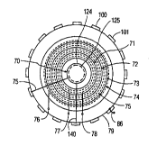
Referring to FIG. 7, there is shown one type of ~ larull.l
conf~guration which can be i~ r~l using the secondary winding structures
depicted in FIGS. I to 6 above. In the ~l~-larul ll.. structure of FIG .7there is shown
a plurality of secondary windings, each of which is formed from a planar composite
sheet, as sheet 10 of FIG. 1 and of ;lUplUpli~, length and which, surrounds a central
WO 94/14174 i PCT/US93111919 --
2~s09~3 12
or center primary cylinder 70. The separate secondary sheets are positioned about the
primary cylinder 70 in concentric circles. Edch of the dark lines as 71, 72 and 73
represent the magnetic sheets or the planar sheets as 12, while the dashed linesrepresent the outer current sheets such as sheets 11 and 13. It is of course understood
that in order to avoid electrical shorts, the respective sheets can be insulated by
covering the exposed surfaces with paper or other insulators. In a similar manner the
sheets can be arranged, as shown in ~IG. 7, and separated by placing a suitable
shellac or other insulating material over the conductive line pattern.
Thus in the ~Idll~rOIIll-l ~illdll~ of FIG. 7 the secondary wiDdin~s
are plallar sheets as those shown in FIGS. I to 6 each arran~ed in concentric circles
about a primary cylinder 70. i~ach separate secondary windings sheet has two
terrninals as 77 and 78 which are available via suitable leads or wires. The primary
cylinder 70 is comprised of a flexible sheet such as sheet 70 shown in FIG. 9. The
insulator sheet 70 of FIG. 9 is fabricated from a suitable paper and has deposited on
the surface a plurality of parallel conductive lines as 125, 126, 127 and 129. The
conductive lines are shown as vertically oriented but can be at slight an~les and are
parallel to each other. The conductor lines teri-ninate in top and bottom land areas,
as land areas 121 and 123 for conductor 125, and top land area 122 and bonom land
area 124 for conductor 126 and so on. Fach conductor of the plurality has such land
areas. The llexible primary sheet is bent or flexed into a circular l,V~jr~ a~iu~ and
placed in the center of a secondary winding di~dll~ tO forin one portion of the
primary winding. As shown in FIG. 7, the conductors 124 and 125, are arranged onthe inside of the concentric cylindrical primary structure 70. The conductive lines can
also be arranged on the outside as well.
A second component of the primary winding consists in an outer
concentric circular planar member 79 which again is fabricated from an insulatorsheet and has deposited ~n a surface thereof larger or wider conductive areas as 100
and 101. The number of conductive lines or areas on the outer primary cylindrical
structure is the same as the number of conductive lines on the inner cylindrical
~ wo 94114174 2 ~ ~ O 9 ~ 3 PCT/US93111919
13
structu}e 70. As shown in FIG. 10, Ihe outer primary member 79 has parallel
conductive lines 100, 101 and 102 each haYing land areas as 130 and 131 associated
with conductor 102, land areas 132 and 133 associated with conductor 101 and so on.
As will be explained, the outer primary cylindrical structure 79 is
connected to the inner primary cylindrical structure 70 by means of suitable
conductors which may be located on cap members. The conductive line patterns arecormected togelher by means of conductive paths to form a continuous coiled primary
winding which overlays the secondary winding. Conductors are directed from a inner
primary conductive line as 127 on member 70 to an outer primary conductive line as
conductor 101 on the outer ring 79. This is shown srhPm~irsllly in FIG. 7 by referring
to conductor 140.
Referring to FIG. 11 the inner primary cylinder 70 and the outer
primary cylinder 79 are shown with a secondary . .lllrlylllAlinl~ shown in dashed lines
positioned LU~ lly between the primary cylinders. The arrows in the figure
show the direction of nux flow through the secondary. Current flOws in the primary
conductors, as for example in the primary center cylinder 70, into the paper as shown
by the cross at the center. Current nOws in the outer primary conductor, as
conductors 100,102 and 101, out from the paper. Hence primary current nOws into
tne conductors of the central conductor 70 in a direction in the paper and out from
the paper in conductors as 100, 101, 102. The conductors are arranged as follows:
Conductor 102 with top terminal 130 is connected to an inner conductor of cylinder
70 at the top terminal of the inner conductor. The bottom terminal of the inner
conductor is then corlnected to a suitable bottom terminal for example of conductor
100 where the top terminal of conductor 100, as terminal 133, is connected to the top
terminal of the next conductor in the line with the bottom terminal of the next
- conductor connected to the bottom terminal of conductor 101 and so on. This, as one
will unfipr~rl~n~i~ creates a coil pattern where the wires or c~nnPrtnrc, as 140 and 141
for example, are directed about the secondary ~ .r~..".~ as for example secondary
windings 71, 72, 73 of FIG. 7. In this manner, a suitable electric field is induced to
Wo 94/14174 21~ 0 9 ~ ~ PCT/US93111919
14
enable current flow in the primary winding to cause in current flow in the secondary
windings. It is of course understood that ~ JIU~II' ' terminals such as terminal 75
associated with the iMer cylinder 70 and terminal 86 associated with the outer
cylinder 79 provide the input terminals for the primary winding.
S Referring to FIG. 12 there is sflown a cap which may be fabricated from
a suitable insulative material such as a ceramic, paper, cardboard or other material.
Formed ûn the bottom side of the cap, are a series of conductive land areas which are
positioned near the outer peripheral of the cap, as conductors 152 and 155. Eachouter land area is coMected to an iMer land or terminal area. Thus. iMer
conductive area 153 is coMected to outer conductive area 151 by means of the
conductive line 152. Each outer conductive area is coMected to an iMer conductive
area by a radial conductive lines as 152,156,158 and so on. The cap 150 constitutes
a COMection cap or a coMectOr which coMects the outer or top terminals of primary
cylinder 79 to the outer or top terminals of primary cylinder 70. In a similar manner,
a bottom cap, which is configured or cap 150, constitutes another conductive pattern
which operates to connect alternate bonom conductors of the iMer and ou~er primary
cylinders to form an alternating or coiled pattern. The cap members are shown inFIG. 13 where a top cap 150T, and a bottom cap 150B are shown positioned with
respect to the iMer and outer primary cylinders 70 and 79. The caps, as indicated,
coMect the top land areas of the outer primary cylinder 79 to the ~ ylut~ , landareas of the iMer primary cylinder 70. Reference numerals 160 and 161, indicate the
positions of the secondary winding sheets as shown in Fig. 7 or Fig. 8.
In FIG. 8, there is shown a spiral confi~lr~ion where one elongated
member, as member 10 of FIG. 1, is arranged in a spiral coiled panern to form a
secondary which is directed around a primary cylindrical member 80 associated with
a primary outer cylinder 88. The primary has input terminals 83 and 84. The primary
winding is structured exactly as the above-described primary consisting of primary
cylinders 70 and 79 and is i~ u~ ,L~d in the same maMer, including caps as
shown in FIG. 12 and FIG. 13, for example or by wires.
~ WO 94114174 215 0 9 ~ 3 PCT/US93/11919
Referring to FIG. 14 the}e is shown an en~irely different transformer
configuration which essen~ially is ;.,.I,l..".. ~ from the flexible conductive planar
sheets as described. above. As seen in the top view of FIG. 14, there is shown aprimary cylinder 160 and a primary cylinder 161. Each of the cylinders as 160 and 161
has the ,."lr~".,.,;,,l, shown in FIG. 9 and essentially each corlsists of a planar flexible
sheet, as sheet 70 of FIG. 9, having a plurality of parallel conductive lines, as
conductors 125, 126 and 127. Each of the primary cylinders are surrounded by a
suitable secondary structure. such as the secondary structure shown in FIG. 7 or the
secondary structure shown in FIG. 8. The conductive lines of each cylinder, are
connected together by means of wires or by means of top and bottom caps to form
a coil or a primary winding where current flows in the directions of the arrows shown.
The flux flow induces secondary currents to flow in the secondary structures 162 and
163. The primary winding has input terminals 170 and 171. Also shown in dashed
lines is a third secondary ~ullri~ul~llioll 165 which essentially is the secondary
configuration, as shown in FIGS. 7 and 8.
FIG. 15 shows the primary winding 180 with output terminals 171 and
170 in a schematic form which primary winding is now surrounded by secondary
windings as 181, 182, 183 and 184. Shown in FIG. 15 are four secondary windings
each of which may have a ..:...r,.... ~ ll shown in FIG. 7 or the ~ ri~ iOI~ shown
in FIG. 8. It is seen that current flowing in the primary winding, which consists of
four cylinders, connected together as described, induces current in the secondary
windings as shown in FIG. 15.
Referring to FIG. 16, there is shown a circuit configuration of the
transformer AIIAI.~,. rl-- '-1 shown in FIG. 7. As seen, the Ll~ ru,-ll~l consists of a
prirnary winding having input terminals 75 and 86. The primary winding 90 is
i...l,l-.,....: ~I by means of the central cylinder 70 and the outer cylinder 79 of FIG.
7. There are a plurality of secondary windings as windings 91, 92 and 93, each of
which is formed from a separate, concentric, lamina sheet such as sheets 71, 72, 73
and so on of FIG. 7. Each of the separate secondary windings as indicated have two
L: ~
WO 94114174 2 i S ~ 9 S 3 PCTIUS93/1 1919
16
terminals and can be illLtl~ulul~ by means ûf diodes or rectifiers, such as 101,shown connecting one terminal of secondary winding 92 to one terminal of secondary
winding 91.
Referring to FIG. 17, there is shown a schematic diagram depicting a
S circuit cr~nf~ rAtinn of the transformer ,~ shown in FIG. 8. As se~n, the
primary winding 95 has input terminals 83 and 84 and is associated with a large
secondary winding 96 having terminals 81 and 82, which winding 96 consists of the
spiral winding having many turns and therefore is capable of extremely high volta~e
step-up ratios.
As one can ascenain from FIGS. 7 and 8, the l,d,,aru.,,,.l shown utilize
rolled flexible planar sheets, essentially are rolled up employing similar techniques
used in forming capacitors. Such Lld.larul~ are extremely reliable and possess
many features which are not found in ~:UII~ iOlldl lldllarUIlll.la. The transformers
exhibit a higher efficiency in the range of 95% or greater and exhibit extremely good
voltage regulation of about 0.97Mohms. These l~dll~rull~.~.ls have high frequency
responses to 100 kHz. The ~ Ilarullll~,la have extremely good eMciency and a very
optimum usage of Lldllarullll~l materials based on their CullaLIu~liull. As one will
n~ r~t~nrl a secondary core is fabricated with a number of concentric and
t~ ,u~ thin anmular rings, as for example shown in FIG. 7. Each of the rings is
capable of ~ o~ a maximum number of current carrying conductors, such
as 11 and 13 of FIG. 1. Thus the core material which is evidenced by planar member
12 of FIG. l is fully and most efficiently excited. The result is a much higher
attainable voltage than can be realized with a single prior art core with one winding.
It is also indicated that the planar sheets are folded in an annular or
concentric ring patterns with an input terminal, as for example 31, providing one
terminal of a secondary winding and the output terminal 35 providing the second
output terrninal. As indicated, these windings can be directly connected together to
form a single secondary winding or can be connected by means of rectifiers. For a
~ wO 94/14174 21 S O 9 ~ 3 PCT/US93/11919
17
given primary excitation with a single prior art secondary core and winding, theop~imum ratio of the two radii for the higher secondary voltage is 1.6487. At thc
same ratio, the attainable secondary voltage with a secondary core comprised of a
given number of concentric planar sheets, as for example shown in FIG. 7, is 1.718
times higher. The available secondary voltage from the improved devices is three or
four times higher than that obtained with conventional Lldl,~ru..~
Improved operation is also due to the fact that the current excitation is
provided via the wireless tapes or planar members which have evaporated conductors
on the surface and which closely couple to the central magnetic sheet or magnetic
member resulting in practically no local leakage for the Lldll~ru.l.l~,.. Thus the
lldll~rullll~., while being extremely efhcient, isextremely small ~ull~;d..illg the voltage
levels operated on.