Note: Descriptions are shown in the official language in which they were submitted.
POWER AMPLIFIER WITH CLIPPING LEVEL CONTROL
BACKGROUND OF THE INVENTION
The invention relates to a solid state power
amplifier which emulates tube distortion. In
particular, the invention relates to a solid state
power amplifier having a tube distortion circuit in
which the power level of the amplifier may be
continually varied while maintaining an appropriate
tube distortion sound.
It is desirable to control the output capability
of a power amplifier. It is particularly desirable for
many musicians to use the power amplifier itself as the
major contribution to the so-called tube distorted
sound. Their desire is to have a high power amplifier
capability for high level stage performances, and at
the same time, a low power amplifier capability for
studio performance. Many contemporary tube power
amplifiers have a high/low switch for such purpose.
Most solid state power amplifiers do not offer this
feature. It is thus desirable to provide a variable
power output and particularly a continuously variable
output power capability in a power amplifier.
SUMMARY OF THE INVENTION
The invention is based upon the discovery that a
limiting circuit may be employed between a first
amplifier stage and a high-gain power amplifier stage
~1~100~~
to limit the output power. A control circuit coupled between
feedback circuits of each amplifier stage is operative to increase
the gain of the first amplifier as the other is decreased and vice
versa. As a result, the effect of the limiting circuit increases
with increasing gain of the first amplifier and decreases with
decreasing gain thereof.
The invention pertains to an amplifier comprising a first
amplifier stage having an input, an output and a feedback circuit
and having a first gain for producing an output. A second
amplifier stage has an input, an output and a feedback circuit and
has a second gain for producing relatively high power output and
having inherent clipping distortion at relatively high power
output, the first and second gains together resulting in a gain
structure for the amplifier. Limit means having a clipping level,
is coupled between the output of the first amplifier stage and
input of the second amplifier stage operative for limiting input
voltage to the second amplifier stage above the clipping level of
the limit means when the gain of the first amplifier stage is
relatively high and when the gain of the second amplifier stage is
relatively low. Tube dynamics control means is coupled between
the feedback circuit of the first amplifier stage and the feedback
circuit of the second amplifier stage for simultaneously changing
feedback impedance in the respective feedback circuits in opposite
first and second directions while maintaining the gain structure.
The control means is operative in the first direction for raising
the gain of the first amplifier and rendering the limit means
operative and reducing the gain of the second amplifier stage and
consequently reducing the output power thereof and for operation
';: _ 2 _
15~100~
in the second direction increasing the gain of the second
amplifier stage for allowing the introduction of the inherent
clipping distortion and for lowering the gain of the first
amplifier stage. With respect to the tube dynamics control means,
it is desirable to operate it so that the overall gain of the
structure is preserved. In an alternative embodiment, the limit
means includes crossover distortion means for emulating tube
compression.
In a particular embodiment, the invention is directed to an
amplifier comprising a first amplifier stage having an input and
an output and a feedback circuit, a power amplifier stage
exhibiting inherent clipping distortion at high power outputs and
having an input and an output and a feedback circuit and a
limiting circuit coupled between the input of the power amplifier
and the output of the first amplifier for limiting the input to
the power amplifier stage. A tube dynamics control is coupled
between feedback circuits for simultaneously changing feedback
impedance in the corresponding feedback circuit of the first
amplifier and the power amplifier in opposite directions.
In an exemplary embodiment, the tube dynamics control
comprises an impedance in the form of a dual
ganged potentiometer or a dual gang resistor and
the limiting circuit is a diode clipping network.
The limiting circuit may also include a compression
circuit. The system may further include a presence and
- 2A -
~, ~.k!~~).
2~,5~~Q3
resonance circuit which operates to control the damping
factor of the load circuit . The system may yet further
include a ripple filter for reducing ripple distortion
associated with the power amplifier at full power
output.
BRIEF DESCRIPTION OF THE DRAWINGS
Fig. 1 is a schematic block diagram broadly
illustrating the concept of the present invention;
Fig. 2 is a schematic diagram illustrating in
greater detail the concept of the present invention
with a simplified limiting circuit;
Fig. 3 is a schematic diagram similar to the
arrangement of Fig. 2 further employing a ripple filter
for reducing annoying line hum introduced during high
power operation;
Fig. 4 is a schematic diagram of the invention
similar to Fig. 3 in which a compression circuit is
combined with the limiting circuit for introducing
controlled cross-over distortion; and
Fig. 5 is a schematic diagram combining elements
of Figs. 3 and 4 and further including a presence and
resonance circuit for varying the damping factor of the
load.
- 3 -
2~~~.~(~3
DESCRIPTION OF THE INVENTION
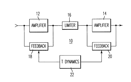
A variable output solid state power amplifier 10
according to the present invention is illustrated in
Fig. 1. The amplifier 10 comprises a first amplifier
stage 12 having an input and an output, a power
amplifier stage 14 having a corresponding input and
output, and a limit circuit 16 coupled between the
output of the first amplifier 12 and the input of the
power amplifier 14, as illustrated. The limit circuit
16 has an output voltage limit which limits the input
to the power amplifier stage 14. Each amplifier 12 and
14 has a corresponding feedback circuit 18 and 20
coupled in feedback relationship between the
corresponding input and output, as illustrated. An
impedance control 22 is coupled between the feedback
circuits 18 and 20. The impedance control or tube
dynamics control (hereinafter T Dynamics) 22 is
operative to introduce a decreasing impedance into
feedback circuit 18 while at the same time increasing
the impedance of the feedback circuit 20 and vice
versa. In the exemplary embodiment, T Dynamics control
22 introduces a low impedance into the feedback circuit
18 of amplifier 12 causing a corresponding increase in
its gain. At the same time, T Dynamics control 22
introduces a high impedance in the feedback circuit 20
of power amplifier 14 which causes its gain to decrease
to a minimum. The power amplifier 14 has inherent
- 4 -
clipping distortion at full power output which is
manifested when the power amplifier 14 is at relatively
high gain.
The limit circuit 16 is operative to limit the
input signal to the power amplifier 14 when the gain of
first amplifier 12 is increased and when the gain of
the power amplifier 14 is decreased. In accordance
with the invention, increasing the gain of amplifier 12
causes an increase in its output until the voltage
limit of limit circuit 16 is reached. Thereafter, any
further increase in signal level is unchanged at the
input of power amplifier 14. In other words, the
signal to the power amplifier 14 is clipped or limited.
The T Dynamics control 22 is thus operative to allow
the system to operate at a relatively low power level
for good studio performance. When it is desired to
increase the power level for stage performance, the
gain of the first amplifier stage is reduced thereby
reducing the effect of the limit circuit 16 and the
gain of the power amplifier of 14 is simultaneously
increased allowing it to produce its own inherent
clipping distortion.
Fig. 2 illustrates in greater detail an exemplary
embodiment of an amplifier system 30 similar to the
arrangement of Fig. 1, wherein similar elements have
the same reference numbers. The amplifier 30 employs
first and second amplifier stages 12 and 14, limit
- 5 -
circuit 16, first and second feedback circuits 18 and
20, and T Dynamics control circuit 22. Amplifier 12
comprises an operational amplifier UlA, and amplifier
14 comprises a driven supply class-B power amplifier
U2B with an operational amplifier driver U1B. The T
Dynamics control 22 is coupled between the
corresponding feedback circuits 18 and 20 of the
operational amplifiers UlA and U1B, as illustrated.
In the circuit of Fig. 2, an input signal I is
coupled through coupling capacitor C1 into the non-
inverted input of operational amplifier UlA. Resistor
R1 is commonly coupled with the capacitor C1 through
non-inverting input of UlA to establish a ground
reference. The first feedback circuit 18 of
operational amplifier UA1 comprises series resistors R3
and R5 coupled between the output and the inverting
input of amplifier UlA. Series connected capacitor C2
and resistor R2 are coupled between the inverting input
of UlA and ground. Capacitor C2 provides DC blocking
for resistor R2. Capacitor C3, coupled across the
amplifier UlA, provides high frequency roll-off
stability.
Resistor R19, associated with the feedback circuit
18, is coupled to the inverting input of UlA and the
load L (e. g., speaker) and provides an overall voltage
feedback path for the amplifier 30. Resistor R20 is
likewise connected between the input of UlA and the
- 6 -
load L for providing a current feedback path for the
amplifier 30. Resistor R4 is coupled at a common node
between the feedback resistors R3 and R5 to the
impedance control 22 for limiting the maximum gain of
the amplifier UlA. Capacitor C12, coupled across
resistor R19, provides high frequency roll-off
stability.
The T Dynamics control 22 includes a pair of
ganged potentiometers VR1A and VR1B. When in the full
clockwise position (CW), VR1A introduces maximum
resistance (e. g., 10K ohm) into the circuit, and VR1B
is at zero ohm. Likewise, at.full counterclockwise
position (CCW), VR1A is zero and VR1B is at maximum
resistance (e. g., 10K ohm). Resistor R23 is coupled
across VR1B to provide a minimum resistance in the
feedback circuit of amplifier U1B, and thus provide a
minimum gain characteristic therefor. When the
impedance control 22 is turned full clockwise (CW), as
noted above, VR1A is at its maximum value (e.g., 10k
ohms). This setting results in a minimum gain value
for operational amplifier UlA.
The signal across the limit circuit 16 is coupled
through coupling capacitor C5 to the inverting input of
the operational amplifier U1B in the power amplifier
14. Resistor R7 is coupled between the inverting input
of U1B and ground providing a ground reference.
Capacitor C6 is coupled between the output and the
inverting input of U1B, providing high frequency roll-
off stability.
In the arrangement illustrated in Fig. 2, limit
circuit 16 comprises parallel diodes CR1 and CR2
connected in opposite polarity or back-to-back
configuration. The operational amplifier. UlA is
coupled through coupling capacitor C4 and series
resistor R6 to the limit circuit 16. The diodes CR1
and CR2 in the distortion circuit 16 serve as signal
clippers whenever the signal conditions at this point
are above the forward drop of the diodes (e. g., +/-0.6v
peak). In other words, as its gain is increased, the
output of amplifier 12 is ultimately constrained to the
limit set by limit circuit 16. This, in turn, limits
the input voltage to power amplifier 14 and thus limits
overall system output.
Amplifier U1B is operative as a predriver for
amplifier U2B, which in the exemplary embodiment is a
complementary connected class-B amplifier. In the
arrangement illustrated, resistors R8 and R10 act as
drive resistors. Parallel connected diode CR3 and
resistor R9 in series with diodes CR4 and CRS,
establish a bias network between the drive resistors.
Complementary drivers Q3 and Q4 are Darlington
connected with complementary connected output devices
Q5 and Q6 and the drive resistors R8 and R10,
respectively. Complementary current limiting devices
- g _
21~~.f~~
Q1 and Q2 are coupled between the base circuit of
drivers Q3 and Q4 and the corresponding emitter
circuits of the output devices Q5 and Q6.
Complementary diodes CR6 and CR7 are coupled in the
base-collector circuit of the drivers Q3 and Q4 and the
current limiting devices Q1 and Q2. Resistors R11, R12
and R15, R16 are connected, as shown, as are
complementary filter capacitors C9 and C10.
A bridge rectifier R circuit comprising diodes
CR8-CR11 are coupled to a power transformer T.
Capacitors C7 and CS in the base collector circuit of
the drivers Q3 and Q4 provide high frequency roll-off
stability.
Operational amplifier U1B has a feedback circuit
20 which includes resistor R22 connected between the
noninverting input and the load L. The resistor 22
provides a secondary overall feedback path for the
amplifier 30. Resistor R21 is connected between the
noninverting input of amplifier U1B and the variable
resistor VR1B of impedance control 22. Resistor R21
limits the maximum gain of the amplifier U1B.
Capacitor C14, coupled between the noninverting input
of U1B and the load L, provides high frequency roll-off
stability. Capacitor C13, coupled between the
noninverting input and resistor R21, provides DC
blocking for resistor R21.
g _
Capacitor C11 is coupled in the secondary of the
power transformer T and protects the bridge rectifier
diodes CR8-CR11 from spike of voltages. When the
impedance control circuit 22 is turned full clockwise
(CW), variable resistor VR1B is at its minimum (zero
ohms) which thereby results in a maximum gain for the
amplifier U1B.
Resistor R24 is coupled between the load L and
ground and provides output current sampling. Resistor
R24 thus provides current feedback to reduce the
damping factor of the amplifier 30 to a value which is
similar to a tube type amplifier, for example, the
damping factor is about one. As noted above, resistor
R23 is coupled across the variable resistor VR1B to
establish a minimum gain value for the operational
amplifier U1B.
Having generally discussed the individual circuit
components, the overall system operation and the
interaction of the T Dynamics control 22 is discussed
in greater detail below. Exemplary circuit component
values are provided for illustration of the concept.
Other values may be employed as desired.
Repeating the previous setting, full clockwise
(CW) (or maximum setting), VR1A is at 10 K ohms and
VR1B is at zero. Thus UlA is at its minimum gain value
and U1B is at its maximum gain value. The exemplary
power amplifier 30 illustrated is intended to deliver
- 10 -
2~.~~~
approximately 50 WRMS into 8 ohms. Thus, this
amplifier will deliver about 20 VRMS to the load L.
Operational amplifier U1B has an feedback resistance
(R22) of 100 K ohms and a resistance to ground (R21 +
VR1B) of 1K (the impedance VR1B is currently at zero
ohms). Thus, the gain of U1B is 101 (i.e., R22/R21 +
1). Hence, the input level at U1B is about 0.2 VRMS
(20/101), or 0.282 volts peak. This level is
considerably below the forward conduction level of
diodes CR1 and CR2 in limit circuit 16. Consequently,
the power amplifier 30 is capable of delivering 20 VRMS
to the load L without the diodes CR1 and CR2 clipping
the signal. Now, UlA is at its minimum gain value.
Calculating the actual gain value of this stage is
difficult since both major current and voltage feedback
signals are returned to UlA via R19 and R20. However,
it can be shown, when using the values provided, that
the input sensitivity is about 1 VRMS at the input of
UlA, and the overall system gain is about 20.
The circuit operation is now discussed with the T
Dynamics control 22 set at full counterclockwise (CCW)
(or minimum setting) . VR1A is now at its minimum value
(or in this case, zero ohms), and VR1B is at its
maximum value of lOK ohms (resistor R23 is ignored for
the moment). The amplifier 30 is again 50 WRMS into 8
ohm which delivers 20 VRMS to the load L. Operational
amplifier U1B has an output feedback resistance (R22)
- 11 -
21~~~fl
of 100K ohms. However, the resistance to ground (R21
and VR1B) is 11K (the VR1B resistance is 10K ohms).
Thus, the gain of U1B is about 9.09 (the gain being
(R22/R21 + VR1B + 1). Hence, the input level at U1B is
2.20 VRMS (20/9.09) or about 3.11 volts peak. This
level is considerably above the forward conduction
level of CR1 and CR2, the clipper diodes, and thus they
will prevent the power amplifier from delivering 20
VRMS to the load. Since the diodes clip at +-0.6 volts
peak and the gain structure is 9.09, and the power
amplifier delivers only about 5.45 volts peak signal to
the load L. If input signals are reduced to where
clipping is just beginning, there would be 0.42 VRMS at
the diodes CRl and CR2 and 3.85 VRMS (or 1.85 WRMS) at
the power amplifier output. Thus, at the full CCW
setting of the T Dynamics control 22, the power
amplifier 14 delivers slightly less than 2 WRMS to the
load "clean".
For most musicians, 2 WRMS is too low to be
practical. Accordingly, resistor R23 is provided in
parallel with VR1B section of the T Dynamics control 22
to thereby establish a minimum resistance to ground.
It can be appreciated that the gain structure is now
about 17, and the power amplifier will deliver about 7
WRMS to the load L "clean". This is a more practical
minimum output level.
- 12 -
Referring again to operational amplifier UlA, at
maximum gain, calculating the actual gain value of this
stage is difficult for the same reasons as set forth
above. However, it can be shown when using the
designed values of Fig. 2, that the input sensitivity
at UlA remains at about 1 VRMS, and the overall system
gain is still at a value of about 20, below clipping as
intended. Thus, at output levels below clipping of
either the power amplifier 14 itself or the clipping
diodes CR1-CR2, the gain structure of the overall
amplifier 30 is the same regardless of whether the T
Dynamics control 22 is set to maximum or to minimum.
The gain structure of the amplifier 30 can be
maintained to about the same value for any setting of
the T Dynamics control 22 by selecting the taper of the
T Dynamics pot sections VR1A and VR1B. For the shown
design, a 20 o audio taper on VRlA and a 20% reverse
audio taper on VR1B is effective. Thus, the T Dynamics
control 22 becomes a power output adjustment, not
simply a gain adjustment. The gain remains constant.
To a musician, this means that the dynamics of the
overload (clipping) point of the power amplifier may be
adjusted. This is a desirable feature to have in any
guitar amplifier, and this is achieved by means of the
gang pot used for the T Dynamics control 22. One
section controls the input gain, one section controls
the power amplifier gain. By careful design, the
- 13 -
~~~~aa
overall gain is nearly always the same regardless of
the control setting. Also, as the control setting is
reduced, a clipping function will begin to limit the
output power in direct proportion to the control
setting.
Additional features of the invention are discussed
with respect to the Figs. 3-6. The reference numerals
for similar elements described in the previous figures
are retained. Reference numerals have been added or
deleted as necessary when corresponding elements have
been added or deleted from Fig. 2.
Fig. 3 illustrates an amplifier 40 similar to the
arrangement of Fig. 2 except for the addition of two
decoupling resistors R25 and R26, and two filter
capacitors C15 and C16. These components are added to
provide an important feature not found on most typical
solid state power amplifiers. This feature is the
elimination of the power supply hum component
introduced into the output signal of most guitar power
amplifiers at clipping.
Whenever a typical solid state power amp clips
(the output swing exceeds the power supply rail
voltage). the power supply ripple signal modulates the
peak output swing of the amplifier, causing an annoying
introduction of a 120 Hz (full wave rectified 60 Hz
mains) hum signal into the guitar amplifier output.
This is noticeable in the sound at full power levels.
- 14 -
2151~~~
Most manufacturers simply cannot afford to use
extremely large values of power supply capacitors
necessary to reduce the hum modulation signals to below
that which is objectionable to most musicians. Also,
this modulation problem usually occurs only at full
power output. Operation at power levels below clipping
does not produce these undesirable results. Also, of
note is that most tube power amplifiers, because they
operate at high voltages and lower currents, have
proportionally lower power supply ripple values, and
thus generally produce less annoying hum generation
type problems at clipping than do their solid state
amplifier counterparts.
By introducing a decoupling resistor and an
additional filter capacitor for the corresponding
supply rails of the drivers Q3 and Q4, the hum
component introduced at clipping is thus reduced
significantly to below the annoyance level for most
musicians.
In the exemplary embodiment, the main power supply
capacitors C9 and C10 are 2200 UF. The added
capacitors C15 and C16 are only 220 UF. However, the
resultant reduction in hum component introduction at
clipping is better than if the main power supply
capacitors were increased to 10,000 OF (four times the
original size). This then offers a more economical
solution to the problem. The only disadvantage to this
- 15 -
215~~~3
approach is the slight reduction in overall continuous
power output capability due to the voltage drop in the
decoupling resistors R25 and R26. For the values used
in the exemplary embodiment, the original 50 WRMS
output power capability was reduced to about 44 WRMS
(or about -0.5 dB in output level) this is a small
reduction in output power, in view of the overall
improved performance.
The value of resistors R25 and R26 should be large
enough so as to offer the extra filter capacitors C15
and C16 an adequate impedance with which to work; and
at the same time R25 and R26 should not be too large as
to further reduce the output power capability of the
amplifier 30 itself. The value of capacitors C9 and
C10 should be large enough to provide the adequate
filtering to eliminate the hum component in the output .
The circuit arrangement of Fig. 3 also offers an
additional advantage in the music power rating of the
power amplifier 14. Music power is the instantaneous
output power capability measured in WRMS that the
system will deliver to the load L for a short period of
time until the supply voltages stored in the capacitors
sag under a continuous loading condition. This rating
usually determines how loud a particular power
amplifier will sound to the musician or just how much
so-called "kick" it has under transient conditions.
Most typical tube power amplifiers have a much higher
- 16 -
music power rating than a solid state counterpart of
the same continuous WRMS rating. It is not uncommon
for a 50 WRMS tube power amp to deliver 200 WRMS music
power. This is why most musicians consider a tube
power amplifier superior for guitar applications.
Tubes deliver more music (or transient) power, and yet
are far easier on the associated loudspeaker whose
failure mechanism is more related to continuous WRMS
rather than music WRMS.
At idle conditions, the extra filter capacitors
C15 and C16 are charged up to the same voltage as the
main filter capacitors C9 and C10, so the music power
rating is unaffected by the addition of this circuitry.
At full continuous operation, however, resistors R25
and R26 drop the voltage level supplied to the drivers
Q3 and Q4 with the resulting power loss as outlined
above . This then makes this solid state power amp have
a music to continuous WRMS ratio closer to that of a
tube power amplifier.
It should be noted that whenever the T Dynamics
control 22 is at the maximum setting, the power
amplifier 14 is clipped at maximum output.
Accordingly, the hum reduction feature described herein
comes into play to eliminate the ripple noise.
However, whenever the T Dynamics control 22 is at a
setting other than maximum, the internal clipping
function limits the output swing, and thus the
- 17 -
amplifier output swing is prevented from reaching the rails.
Fig. 4 illustrates an amplifier 50 incorporating another
feature of the invention wherein a compression circuit 52 is
combined in the limiting circuit 16. In the arrangement
illustrated, the clipping diodes CR1 and CR2 (Fig. 3) are replaced
with a compression circuit 32 similar to the arrangement disclosed
in Canadian Patent Application "Solid State Tube Compression
Circuit", File No. 2,139,7l4 filed January 6, l995, assigned to
the assignee herein. This modification provides means to create
a tube compression effect as outlined in the application and at
the same time produces limiting means to control or change the
output power level at which the tube compression effect takes
place. In the arrangement of Fig. 3, the T Dynamics control 22 is
effective to change the gain structure of the circuitry
around the clipping diodes CR1 and CR2. T Dynamics
control causes diodes CR1 and CR2 to clip the sianal at
output power levels below full power, while maintaining
the same overall gain structure at output levels below
clipping for any setting of the T Dynamics control 22.
In the arrangement of Fig. 4, the hard clipping
provided by the diodes CRl and CR2 is replaced with a
compression circuit 52 that introduces cross-over
- 18 -
r
distortion resulting in soft, tube-like compression at
clipping. This effect is far more pleasing to
musicians who would desire this feature, and in actual
usage it duplicates very closely the actual operation
in an actual tube type power amplifier. As with the
diodes, the circuitry of Fig. 4 maintains the same
overall gain structure at output levels below clipping
for any setting of the T Dynamics control 22. Thus,
this control is still an effective means to adjust the
power amplifier dynamics to match his playing style for
clipping and overload.
The compression circuit 52 emulates tube
compression associated with an overbiased class-B push-
pull tube amplifier at high input signal levels due to
a f low ~ of current into the grid of the output tubes
resulting in an output clipping characteristic with
crossover distortion. In the embodiment illustrated,
the compression circuit comprises a pair of class-B
connected solid state upper and lower unity gain
operational amplifier devices UlA, U2A, each including
an input circuit and output circuit. The output
circuit of the paired devices are connected for mixing.
In the upper circuit a biasing circuit, including
complementary connected diodes CR12, CR13 and resistors
R29, R30 and R31 establish a clipping level offset at
the input and at the output of each device. The lower
circuit is the same . Clipping devices CR12 and CR16 in
- 19 -
the input circuit and the output circuit respectively
clip the offset at the input and the offset at the
output of each solid state device. A charging device,
capacitor C17 and resistor R27, overbiases the offset
in the input circuit whenever the input signal is
greater than the input clipping device CR12. The
overbiasing causes crossover distortion, emulating the
desirable compression associated with a tube amplifier.
The offset voltage in the exemplary embodiment is a
diode voltage drop, e.g., about 0.6 VDC.
The previous discussions concerning the gain
structure of the power amplifier at various settings of
the T.Dynamics control 22 applies to the arrangement of
Fig. 4 and need not be repeated. Of interest is that
the tube compression circuitry 52 may be defeated by
simply shorting capacitors C17 and C18. When these
capacitors are shorted, the circuitry is essentially
reduced to the diode clipping circuit previously
described, where the diodes CR12 and CR13 in Fig. 4 act
in a similar manner to the diodes CR1 and CR2 in Figs.
2 and 3, as a simple hard clipping means. When
capacitors C17 and C18 are not shorted, the bias
circuitry and various other circuit components come
into play to cause not only clipping, but compression
as outlined in the above-identified patent application.
The T Dynamics control 22 allows flexibility in the
operation of the tube compression circuit 33 by
- 20 -
2151~~~
providing the ability to change the power output level
at which the compression effect occurs.
Fig. 4 also employs the decoupling resistors R25
. and R26 and capacitors C15 and C16 to eliminate the
power supply hum component introduced into the output
signal. Although, not necessary for the successful
operation of the T Dynamics control 22 with the tube
compression circuitry 33, this feature helps to more
fully duplicate a typical tube power amplifier, and
thus it is desirable.
U.S. Patent No. 5,197,102, entitled Frequency
Selective Damping Factor Control, assigned to the
assignee herein, employs two power amplifier controls
in an arrangement called presence and resonance. The
presence control produces a reduction of the damping
factor at high frequencies (1 Khz and above) which
effectively raises the high end response of the
associated loudspeaker system at the frequencies where
the impedance characteristics rises. This offers the
musician a brighter, strident type sound. The
resonance control produces a reduction of the damping
factor at low frequencies (500 Hz and below) which
effectively increases the low end response of the
associated loudspeaker system most noticeably at the
resonance frequency of the enclosure where the
impedance is highest. This offers the musician a
punchy, boomy type sound.
- 21 -
~~~~~a~
Noteworthy features of these controls is their
ability to improve both the high and low end response
' (sounds) of the typical guitar or bass music at low
performance levels (below any power amp clipping), but
at high performance levels (above power amp clipping)
their effects are defeated. To a musician, this means
a bright or punchy type sound may be played softly, but
when the power is increased, the bright does not turn
into so-called "cutting" and the punch does not turn
into "mushy" overload.
In Fig. 5, an amplifier 60 is illustrated in which
the overall power amplifier feedback resistor R19
(Figs. 2-4) is replaced with a frequency selective
network 62 or presence and resonance (P&R) control
comprising resistors R39 and R40, capacitors C19 and
C20, and potentiometers VR2 (the presence control) and
VR3 (the resonance control). When both VR2 and VR3 are
set at their full counterclockwise (CCW) or minimum
setting, the frequency selective network 62 is reduced
to a simple divider resistor network, namely R40, VR2
and R39. This network now offers the same effect as
the resistor R19 (Fig. 4) which is essentially a flat
response with no presence or resonance boost. If
either or both of the controls VR2 and VR3 are set in
any clockwise (boosted) setting, the network 62 offers
an altered frequency response to provide the desired
damping factor reduction in either the high or low
- 22 -
~~~oo~
frequency spectrum. The details of this are more fully discussed
in the aforementioned patent and need not be repeated herein.
Of importance is that the control 62 functions as intended in
the circuit of Fig. 5 and their effects are not altered by changes
in the T Dynamics control 22, because the frequency selective
network 62 connects from system output to system input and the T
Dynamics control 22 is designed to maintain the overall gain value
from input to output. Also, of importance is that the network 62
ceases to function whenever either the power amplifier clips 14 or
when the tube compression circuitry 52 is activated. The network
62 is a feedback function. Both power amplifier clipping and tube
compression circuitry activation limit the feed-forward signal
which then defeats any feedback control. Thus, the T Dynamics
control 22 can set the output power capability of the amplifier
and not alter the functions of the presence and resonance controls
62, but the control functions of the network 62 are defeated at
the clipping level set by the T Dynamics control 22.
The invention may be combined with a preamplifier circuit,
such as disclosed in Canadian Patent Application entitled "Multi-
Stage Solid State Amplifier that Emulates Tube Distortion" File
No. 2,139,717 filed January 6, 1995, assigned to the assignee
herein. The amplifier of the invention may also include a tone
control circuit similar to the presence and resonance circuit or
other tone controls may be employed in addition or in lieu of the
circuit.
While there have been described what are at present
considered to be the preferred embodiments of the present
invention, it will be apparent to those skilled in the art that
- 23 -
Q151 00~
various changes and modifications may be made therein without
departing from the invention and it is intended in the appended
claims to cover such changes and modifications as fall within the
spirit and scope of the invention.
- 24 -