Note: Descriptions are shown in the official language in which they were submitted.
- 21S1199
-
- 1 - CFO 10695 CA
IMAGE-FORMING APPARATUS
AND MANUFACTURE METHOD OF SAME
BACKGROUND OF THE INVENTION
Field of the Invention
The present invention relates to a flat type
image-forming apparatus using electron-emitting
devices, and a manufacture method of the image-forming
apparatus.
Related Backqround Art
Recently, light and thin displays, i.e., the
so-called flat displays, have received widespread
attention as an image-forming apparatus to be used in
place of large and heavy cathode-ray tubes. Liquid
crystal displays have been intensively researched and
developed as typical flat displays, but still have
problems that an image is dark and an angle of the view
field is narrow. Emission type flat displays in which
electron beams emitted from electron-emitting devices
are irradiated to fluorescent substAnc~-~ to generate
fluorescence, thereby forming an image, are also known
as ones expected to be substituted for liquid crystal
displays. The emission type flat displays using the
electron-emitting devices provide a brighter image and
a wider angle of the view field than the liquid crystal
displays. Demand for the emission type flat displays
is increasing because they are also adaptable for
2151199
achie~ nt of larger screen size and finer resolution.
There are known two main types of
electron-emitting devices; i.e., a hot cathode device
and a cold cathode device. Cold cathode devices
include, for example, electron-emitting devices of
field emission type (hereinafter abbreviated to FE), of
metal/insulating layer/metal type (hereinafter
abbreviated to MIM), and of surface conduction type.
Examples of FE electron-emitting devices are described
in, e.g., W.P. Dyke & W.W. Doran, "Field Emission",
Advance in Electron Physics, 8, 89 (1956) and C.A.
Spindt, "Physical properties of thin-film field
emission cathodes with molybdenum cones", J. Appl.
Phys., 47, 5248 (1976).
One example of MIM electron-emitting devices is
described in, e.g., C.A. Mead, "Operation of
Tunnel-Emission Devices", J. Appl. Phys., 32, 646
(1961).
One example of surface conduction
electron-emitting devices is described in, e.g., M.I.
Elinson, Radio Eng. Electron Phys., 10, 1290, (1965).
In a surface conduction electron-emitting device,
when a thin film of small area is formed on a base
plate and a current is supplied to flow parallel to the
film surface, electrons are emitted therefrom. As to
such a surface conduction electron-emitting device,
there have been reported, for example, one using a thin
2151199
film of SnO2 by Elinson cited above, one using an Au
thin film [G. Dittmer: Thin Solid Films, 9, 317
(1972)], one using a thin film of In203/SnO2 [M.
Hartwell and C.G. Fonstad: IEEE Trans. ED Conf., 519
(1975)], and one using a carbon thin film [Hisashi
Araki et al.: Vacuum, Vol. 26, No. 1, 22 (1983)].
As a typical configuration of those surface
conduction electron-emitting devices, Fig. 22
schematically shows the device configuration proposed
by M. Hartwell, et al. in the above-cited paper. In
Fig. 22, denoted by reference numeral 1 is a base plate
and 33 is a conductive thin film made of a metal oxide
formed by sputtering into an H-shaped pattern. The
conductive thin film 33 is subjected to an energizing
process called forming by energization (described
later) to form an electron-emitting region 34.
Incidentally,-the spacing L between device electrodes
31, 32 is set to 0.5 - 1 mm and the width W of the
conductive thin film 33 is set to 0.1 mm.
In those surface conduction electron-emitting
devices, it has heretofore been customary that, before
starting the emission of electrons, the conductive thin
film 33 is subjected to an energizing process called
forming by energization to form the electron-emitting
region 34. The term "forming by energization" means a
process of applying a DC voltage being constant or
rising very slowly across the conductive thin film 33
2151199
to locally destroy, deform or denature it to thereby
form the electron-emitting region 34 which has been
transformed into an electrically high-resistant state.
In the electron-emitting region 34, a crack is produced
in part of the conductive thin film 33 and electrons
are emitted from the vicinity of the crack. Thus, the
surface conduction electron-emitting device after the
forming by energization emits electrons from the
electron-emitting region 34 when an appropriate voltage
is applied to the conductive thin film 33 so that a
current flows through the device.
The surface conduction electron-emitting device is
simple in structure and easy to manufacture, and hence
has an advantage that a number of devices can be formed
into an array having a large area. Therefore, the
application of the surface conduction electron-emitting
device to charged beam sources, displays and so on have
been studied in view of such advantageous features. As
one example of applications in which a number of the
surface conduction electron-emitting devices are formed
into an array, there is proposed an electron source
that, as described later in detail, the surface
conduction electron-emitting devices are arrayed in
parallel, i.e., in the so-called ladder pattern, and
opposite ends of the individual devices are
interconnected by two wirings (called also common
wirings) to form one row, followed by forming this row
~ 21~1199
-- 5 --
in a large number (see, e.g., Japanese Patent
Application Laid-Open No. 64-31332).
The applicant has previously proposed a flat type
image forming apparatus wherein a base plate
(hereinafter referred to also as a rear plate)
including electron-emitting devices formed thereon and
a base plate (hereinafter referred to also as a face
plate) including a fluorescent film formed thereon are
disposed to face each other, a space defined between
both the base plates is evacuated into a depressurized
state (or a vacuum state), and electron beams emitted
from the electron-emitting devices are irradiated to
the fluorescent film to form an image (see, Japanese
Patent Application Laid-Open No. 2-299136).
Fig. 23 schematically shows a section of the above
flat type image forming apparatus using the
electron-emitting devices. In Fig. 23, the apparatus
comprises a rear plate 1, electron-emitting devices 54,
and a pressure bearing member 3 endurable against the
atmospheric pressure. Denoted by 4 is a face plate on
the undersurface of which a fluorescent film 5 and a
metal back 6 are formed. An outer frame 8 is connected
to the face plate 4 and the rear plate 1 through frit
glass 7 in a sealed manner to construct an envelope
(vacuum cont~iner). An inner space in the envelope is
evacuated through a vent tube (not shown) to establish
a depressurized state (or a vacuum state).
2 1 5 1 1 9 9
However, it has been found from studies made by
the inventors that there is still a room for
impLov -nt of the above image forming apparatus in
points below. The presence of the pressure bearing
member endurable against the atmospheric pressure in
the vacuum envelope reduces evacuation conductance.
Therefore, a relatively long time is required to
evacuate the inner space of the envelope. Also, when
the envelope is evacuated in a relatively short time,
there arises a fear that the inner space of the
envelope may not be sufficiently depressurized and a
finally reached vacuum level may be relatively low.
Accordingly, the operation of evacuating the envelope
takes a larger percentage in the production cost. It
is thus concluded that reducing the time required for
evacuating the envelope greatly contributes to cut down
the cost. Also, this effect is expected to become more
remarkable in image-forming apparatus having a larger
display screen size.
SUMMARY OF THE INVENTION
An object of the present invention is to provide
an image-forming apparatus and a manufacture method of
the image-forming apparatus which are able to solve the
above-explained te~hnical problems in the prior art.
Another object of the present invention is to
provide an image-forming apparatus and a manufacture
`- 2151199
method of the image-forming apparatus by which
evacuation conductance can be increased to reduce an
evacuation time.
Still another object of the present invention is
to provide an image-forming apparatus and a manufacture
method of the image-forming apparatus by which a higher
vacuum level can be achieved in an envelope (vacuum
container) to reduce residual gas left in the envelope,
enabling an image to be stably displayed for a long
term.
To achieve the above objects, the image-forming
apparatus of the present invention is arranged as
follows.
The image-forming apparatus according to the
present invention comprises a rear plate including
electron-emitting devices formed thereon, a face plate
including a fluorescent film formed thereon and being
disposed to face the rear plate, a spacer in the form
of a flat plate disposed between the rear plate and the
face plate, and an outer frame surrounding peripheral
edges of the rear plate and the face plate, electrons
emitted from the electron-emitting devices being
irradiated to the fluorescent film to thereby display
an image under condition where an inner space of a
container constructed by the rear plate, the face plate
and the outer frame is evacuated through a vent tube
into a depressurized state, wherein the vent tube is
~ 2151199
att~.he.~ to a side of the outer frame that is
positioned across an imaginary extension of the
flat-plate æpacer in the longitl~;n~l direction
thereof, or to the face plate or the rear plate in the
vicinity of that side of the outer frame.
The present invention also involves a manufacture
method of the image-forming apparatus.
The manufacture method according to the present
invention is a method for manufacturing an image-
forming apparatus comprising a rear plate includingelectron-emitting devices formed thereon, a face plate
including a fluorescent film formed thereon and being
disposed to face the rear plate, a spacer in the form
of a flat plate disposed between the rear plate and the
face plate, and an outer frame surrounding peripheral
edges of the rear plate and the face plate, electrons
emitted from the electron-emitting devices being
irradiated to the fluorescent film to thereby display
an image under condition where an inner space of a
container constructed by the rear plate, the face plate
and the outer frame is evacuated through a vent tube
into a depressurized state, wherein the method
comprises providing a vent tube attached to a side of
the outer frame that is positioned across an imaginary
extension of the flat-plate spacer in the longitll~i n~l
direction thereof, or to the face plate or the rear
plate in the vicinity of that side of the outer frame,
2151199
,_
and evacuating the inner space of the container through
the vent tube.
With the present invention, the above-explained
technical problems in the prior art can be solved and
the foregoing objects can be achieved. With the
manufacture method of the image-forming apparatus of
the present invention, since the vent tube is disposed
in a specific position, evacuation conductance can be
increased to reduce an evacuation time. In addition, a
higher vacuum level can be achieved in the cont~i~er
(envelope).
With the image-forming apparatus of the present
invention, residual gas left in the container
(envelope) space can be reduced to a very small amount
and, therefore, stable image display can be continued
for a long term.
BRIEF DESCRIPTION OF THE DRAWINGS
Fig. 1 is a schematic perspective view, partly
broken away, showing one example of the image-forming
apparatus of the present invention.
Figs. 2 to 12 are schematic views for expl~i~i ng
some embodiments of the image-forming apparatus of the
present invention.
Figs. 13A and 13B are schematic plan and sectional
views, respectively, of a planar type surface
conduction electron-emitting device which can be used
21~1199
-- 10 --
in the present invention.
Fig. 14 is a schematic view showing one example of
a step type surface conduction electron-emitting device
which can be used in the present invention.
Figs. 15A to 15C are schematic views showing
successive manufacture steps of the surface conduction
electron-emitting device.
Figs. 16A and 16B are charts showing examples of
voltage waveform which can be applied in the forming
process by energization to manufacture the surface
conduction electron-emitting device.
Fig. 17 is a schematic view showing an FE
electron-emitting device.
Fig. 18 is a schematic view showing one example of
a base plate for an electron source in a matrix
pattern.
Figs. l9A and l9B are schematic views showing
examples of a fluorescent film.
Fig. 20 is a block diagram showing one example of
a driving circuit adapted to display an image in
accordance with TV signals of NTSC standards.
Fig. 21 is a schematic view showing one example of
a base plate for an electron source in a ladder
pattern.
Fig. 22 is a schematic view of a typical surface
conduction electron-emitting device.
Fig. 23 is a schematic view showing a conventional
2151199
image-forming apparatus using typical surface
conduction electron-emitting devices.
DETAILED DESCRIPTION OF THE PREFERRED EMBODIMENTS
An image-forming apparatus and a manufacture
method of the image-forming apparatus according to the
present invention are basically arranged as set forth
above.
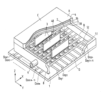
One example of the image-forming apparatus of the
present invention will be described below with
reference to Fig. 1 which schematically shows the
image-forming apparatus of the present invention. In
the image-forming apparatus of Fig. 1, a rear plate 1
including electron-emitting devices 2 formed thereon
and a face plate 4 including a fluorescent film 5
formed thereon are disposed to face each other, and an
outer frame 8 is disposed to surround the face plate 4
and the rear plate 1 along their peripheral edges. A
plurality of spacers 3 in the form of flat plates are
disposed between the face plate 4 and the rear plate 1,
the spacers 3 being bonded to the rear plate 1 by an
adhesive 48. In use of the image-forming apparatus of
the present invention, an inner space of an envelope
(vacuum contAiner) constructed by the face plate 4, the
rear plate 1 and the outer frame 8 is evacuated into a
depressurized state. The spacers 3 are, therefore,
provided to keep the structure of the envelope
_ 2151199
endurable against the atmospheric pressure. A vent
tube 9 through which an inner space of the envelope is
evacuated is att~he~ to a side of the outer frame 8
that is positioned across imaginary extensions of the
flat-plate spacers 3 in the longitll~i n~l direction
thereof. Denoted by 51, 52 are wirings for
interconnecting the electron-emitting devices arrayed
in a matrix pattern. A black film 36 formed of a black
matrix or the like and a metal back 38 are provided, if
required, as shown. While the vent tube 9 is attached
to the side of the outer frame 8 that is positioned
across the imaginary extensions of the flat-plate
spacers 3 in the longitudinal direction thereof, as
explained above, in this embodiment, the attachment
position of the vent tube 9 is not limited to the outer
frame. By way of example, the vent tube 9 may be
att~he~ to the face plate 4 at a position A or the
rear plate 1 at a position B. These positions A and B
belong to areas of the face plate and the rear plate,
respectively, which locate in the vicinity of the side
of the outer frame 8 that is positioned across the
imaginary extensions of the flat-plate spacers 3 in the
longitudinal direction thereof. In this case, however,
it is required that the areas of the face plate and the
rear plate which locate in the vicinity of the side of
the outer frame that is positioned across the imaginary
extensions of the flat-plate spacers in the
2151199
.
- 13 -
longitll~inAl direction thereof be selected so as not to
affect a pixel portion in which an image is formed.
With the present invention, since the vent tube 9
is disposed in the specific position described above,
evacuation conductance can be increased to shorten an
evacuation time, achieve a higher vacuum level, and
hence reduce an amount of residual gas left in the
envelope. If the vent tube is attached to a position C
or D in Fig. 1, the evacuation conductance would not be
so high as that resulted by attaching the vent tube to
the position A or B. Therefore, the present invention
does not involve such an arrangement that the vent tube
is attached to the position C or D. In the present
invention, the number of the vent tube is not limited
to one, but may be plural. Further, the vent tube and
the flat-plate spacers can be positioned in various
combinations as described later.
In the image-forming apparatus shown in Fig. 1,
after evacuating the inner space of the envelope
(vacuum contA;ner) constructed by the face plate 4, the
rear plate 1 and the outer frame 8 through the vent
tube 9, the vent tube 9 is sealed off to maintain the
inner space at a vacuum level on the order of lO-s torr
to 10-8 torr. Under this condition, voltages are
selectively applied through terminals Doxl to Doxm and
Doyl to Doyn to the electron-emitting devices 2,
causing electrons to be emitted from the
~ 21S1199
- 14 -
electron-emitting devices 2. The emitted electrons are
irradiated to the fluorescent film 5 so that
fluorescence is generated from the film 5 to form an
image.
Not only surface conduction electron-emitting
devices, but also hot cathode devices, FE
electron-emitting devices and others can be used as the
electron-emitting devices in the present invention.
While the following description will be made mainly in
connection the case of using surface conduction
electron-emitting devices, the present invention is not
limited to the image-forming apparatus using surface
conduction electron-emitting devices.
Figs. 13A and 13B are a schematic plan and
sectional view, respectively, of a surface conduction
electron-emitting device which can be used in the
present invention.
In Figs. 13A and 13B, denoted by 1 is a base
plate, 31 and 32 are device electrodes, 33 is a
conductive thin film, and 34 is an electron-emitting
region.
The base plate 1 may be any of various glasses
such as quartz glass, glass containing impurities such
as Na in a reduced content, soda lime glass, and glass
having SiO2 laminated thereon by sputtering, or ceramics
such as alumina.
The device electrodes 31, 32 opposed to each other
2151199
- 15 -
can be made of any of usual conductive materials. By
way of example, a material for the device electrodes
may be selected from metals such as Ni, Cr, Au, Mo, W,
Pt, Ti, Al, Cu and Pd or alloys thereof, printed
conductors comprising metals such as Pd, As, Ag, Au,
Ru02 and Pd-Ag or oxides thereof, glass and so on,
transparent conductors such as In203-SnO2, and
semiconductors such as polysilicon.
The spacing L between the device electrodes, the
length W of each device electrode, and the shape of the
conductive thin film 33 are designed in view of the
form of application and other conditions. The spacing
L between the device electrodes is preferably in the
range of several thousands angstroms to several
lS hundreds microns, more preferably in the range of 1 ~m
to 100 ~m, taking into account the voltage applied to
between the device electrodes. The length W of each of
the device electrode 31, 32 is in the range of several
microns to several hundreds microns. The thickness d
of each device electrode is in the range of 100 ~ to 1
~m.
In addition to the structure shown in Figs. 13A
and 13B, the surface conduction electron-emitting
device may also be obtained by laminating one device
electrode 31, the conductive thin film 33, and the
other device electrode 32 on the base plate 1
successively.
2151199
- 16 -
In order to provide good electron-emitting
characteristics, the conductive thin film 33 is
preferably formed of a fine particle film comprising
fine particles. The thickness of the conductive thin
film 33 is appropriately set in consideration of step
coverage to the device electrodes 31, 32, a resistance
value between the device electrodes 31, 32, conditions
of the forming process (described later), and so on.
In general, the thin film is preferably in the range of
several angstroms to several thousands angstroms, more
preferably in the range of 10 A to 500 A. The
conductive thin film 33 has a resistance value
expressed by Rs in the range of 1 x 10² to 1 x 10⁷ Q.
Incidentally, Rs is a value which appears when the
resistance R of a thin film having a thickness t, a
width w and a length 1 is defined by R = Rs(l/w), and
it is represented by Rs = p/t where the resistivity of
a thin film material is p. While the forming process
will be described as being carried out by energization
in this specification, it is not limited to the
energization process, but may be carried out by any
suitable method which can cause a crack in the film to
develop a high-resistance state.
A material used to form the conductive thin film
33 can be appropriately selected from, for example,
metals such as Pd, Pt, Ru, Ag, Au, Ti, In, Cu, Cr, Fe,
Zn, Sn, Ta, W and Pb, oxides such as PdO, SnO2, In203,
2151199
PbO and Sb2O3, borides such as HfB2, ZrB2, LaB6, CeB6, YB4
and GdB4, carbides such as TiC, ZrC, HfC, TaC, SiC and
WC, nitrides such as TiN, ZrN and HfN, semiconductors
such as Si and Ge, and carbon.
The term "fine particle film" used herein means a
film comprising a number of fine particles aggregated
together and having a microstructure that individual
fine particles are dispersed away from each other, or
adjacent to each other, or overlapped with each other
(including a structure where some fine particles are
aggregated and dispersed in island states over the
entire film). The size of the fine particles is in the
range of several angstroms to one micron, more
preferably 10 A to 200 A.
The electron-emitting portion 34 is formed by a
high-resistance crack developed in part of the
conductive thin film 33, and depends on the thickness,
properties and material of the conductive thin film 33,
the manner of the forming process by energization, and
so on. Conductive fine particles having a size not
larger than 1000 A may be contained in the
electron-emitting region 34. The conductive fine
particles contain part or all of elements making up a
material of the conductive thin film 33. The
electron-emitting region 34 and the conductive thin
film 33 in the vicinity thereof may contain carbon or
carbon compounds in some cases.
2151199
Fig. 14 schematically shows one example of a step
type surface conduction electron-emitting device which
can be used in the image-forming apparatus of the
present invention.
In Fig. 14, the same components as those in Figs.
13A and 13B are denoted by the same reference numerals.
Denoted by 35 is a step-forming section. A base plate
1, device electrodes 31 and 32, a conductive thin film
33, and an electron-emitting region 34 can be made of
similar materials as used in the flat-type surface
conduction electron-emitting devices explained above.
The step forming section 35 is formed of, e.g., an
electrically insulating material such as SiO2 by any
suitable process of vacuum evaporation, printing,
sputtering or the like. The thickness of the step
forming section 35 may be in the range of several
thousands angstroms to several microns corresponding to
the spacing L between the device electrodes in the
flat-type surface conduction electron-emitting devices
explained above. While the thickness of a film used to
form the step-forming section 35 is set in
consideration of a manufacture process of the step
forming section 35 and the voltage applied to between
the device electrodes, it is preferably in the range of
several hundreds angs~ to several microns.
The conductive thin film 33 is laminated on the
device electrodes 31, 32 after the device electrodes
2151199
-- 19 --
31, 32 and the step-forming section 35 have been
formed. Although the electron-emitting region 34 is
formed in the step-forming section 35 in Fig. 14, the
shape and position of the electron-emitting region 34
depend on conditions of the manufacture process, the
forming process, etc. and are not limited to
illustrated ones.
While the surface conduction electron-emitting
devices explained above can be manufactured by various
methods, Figs. 15A to 15C schematically shows one
example of the manufacture process.
One example of the manufacture process will be
described below with reference to Figs. 13A and 13B and
Figs. 15A to 15C. In Figs. 15A to 15C, the same
components as those in Figs. 13A and 13B are denoted by
the same reference numerals.
1) The base plate 1 is sufficiently washed with a
detergent, pure water, an organic solvent and the like.
A device electrode material is then deposited on the
base plate by vacuum evaporation, sputtering or the
like. After that, the deposited material is patterned
by photolithography etching to form the device
electrodes 31, 32 (Fig. 15A).
2) Over the base plate 1 having the device electrodes
31, 32 formed thereon, an organic metal solution is
coated to form an organic metal thin film. The organic
metal solution may be of a solution of an organic metal
2151199
- 20 -
compound cont~; n~ ng, as a primary element, a material
metal of the conductive thin film 33. The organic
metal thin film is heated for baking and then patterned
by lift-off, etching or the like to form the conductive
thin film 33 (Fig. 15B). While the organic metal
solution is coated in this example, the process of
forming the conductive thin film 33 is not limited to
coating, but may be carried out by any other suitable
method such as vacuum evaporation, sputtering, chemical
vapor deposition, spi nni ng or spraying.
3) Subse~uently, the base plate including the device
electrodes and the conductive thin film is subjected to
the forming process. A process by energization will be
described here as one example of the forming process.
When an appropriate voltage is applied to between the
device electrodes 31, 32 from a power supply (not
shown), part of the conductive thin film 33 is changed
in its structure to form the electron-emitting region
34 (Fig. 15C). With the forming process by
energization, the conductive thin film 33 is
locally de~lo~ed, deformed or denatured to change the
structure in its part. This part of the conductive
thin film 33 becomes the electron-emitting region 34.
Examples of voltage waveform applied for the forming by
energization are shown in Figs. 16A and 16B.
The voltage waveform is preferably of a pulse-like
waveform. The forming process by energization can be
2151199
- 21 -
performed by applying voltage pulses having a constant
crest value successively as shown in Fig. 16A, or by
applying voltage pulses having crest values gradually
increased as shown in Fig. 16B.
In Fig. 16A, Tl and T2 represent respectively a
pulse width and a pulse interval of the voltage
waveform. Usually, Tl is set to fall in the range of 1
~s to 10 ms and T2 is set to fall in the range of 10 ~us
to 100 ms. A crest value of the triangular waveform
(i.e., a peak value in the forming process by
energization) is appropriately selected depending on
the type of surface conduction electron-emitting
device. Under these conditions, the voltage is applied
for, e.g., several seconds to several tens minutes.
The pulse is not limited to the triangular waveform,
but may have any other desired waveform such as
rectangular one.
In the method shown in Fig. 16B, Tl and T2 can be
set to the similar values as in the method shown in
Fig. 16A. A crest value of the triangular waveform
(i.e., a peak value in the forming process by
energization) is increased, for example, at a rate of
0.1 V per pulse.
The time at which the forming process by
energization is to be completed can be detected by
applying a voltage whose value is so selected as not to
locally destroy or deform the conductive thin film 33,
2151199
and measuring a current during the pulse interval T2.
By way of example, while applying a voltage of about
0.1 V to the device, a resulting device current is
measured to determine a resistance value and, when the
resistance value exceeds 1 MQ, the forming process by
energization is finished.
4) After the forming process by energization, the
electron-emitting device is subjected to an activation
process. The activation process remarkably changes a
device current If and an emission current Ie.
The activation process can be performed by
periodically applying a pulse to the device as with the
forming process by energization, but in an atmosphere
containing gas of an organic material. This atmosphere
is obtained by evacuating the envelope through the vent
tube by an ion pump to create a sufficiently high
degree of vacuum and then introducing gas of a selected
organic material to the vacuum space. A preferable gas
pressure of the organic material depends on the form of
application, the configuration of the envelope (vacuum
container), the kind of organic material, etc. and,
hence, it is appropriately set case by case. Examples
of suitable organic materials include aliphatic
hydrocarbons such as alkanes, alkenes and alkynes,
aromatic hydrocarbons, alcohols, aldehydes, ketones,
amines, and organic acids such as phenol, carboxylic
acid and sulfonic acid. More specifically, the
2151199
suitably usable organic materials are saturated
hydrocarbons expressed by CnH2n+2 such as methane, ethane
and propane, unsaturated hydrocarbons expressed by CnH2n
such as ethylene and propylene, benzene, toluene,
methanol, ethanol, formaldehyde, acetone, methyl ethyl
ketone, methylamine, ethylamine, phenol, formic acid,
acetic acid, propionic acid, etc. As a result of the
activation process, carbon or carbon compounds are
deposited on the device from the organic material
present in the atmosphere so that the device current If
and the emission current Ie are remarkably changed.
The timing to finish the activation process is
determined while measuring the device current If and
the emission current Ie. The width, interval and crest
value of the applied pulse is appropriately set.
The carbon or the carbon compounds are in the form
of graphite such as HOPG (Highly Oriented Pyrolitic
Graphite), PG (Pyrolitic Graphite), and GC (Glassy
Carbon) (HOPG means graphite having a substantially
complete crystal structure, PG means graphite having a
crystal grain size of 200 A and a crystal structure
slightly disordered, and GC means graphite having a
crystal grain size of 20 ~ and a crystal structure more
disordered), or amorphous carbon (including amorphous
carbon alone and a mixture of amorphous carbon and fine
crystals of any above graphite). The thickness of the
2151199
- 24 -
deposited carbon or the carbon compounds is preferably
not larger than 500 A, more preferably not larger than
300 A.
5) It is preferable that the electron-emitting device
after the activation process is subjected to a
stabilization process. The stabilization process is
desirably performed on condition that the organic
material in the vacuum container has a partial pressure
of 1 x 10⁻⁸ torr or less, preferably to 1 x 10⁻¹ torr or
less. The pressure in the vacuum container is
preferably in the range of 10-65 to 10-7 torr, more
preferably 1 x 10⁻⁸ torr or less. An apparatus for
evacuating the vacuum container is preferably of the
type using no oil so that oil generated from the
evacuation apparatus will not affect characteristics of
the electron-emitting device. Practical examples of
the evacuation apparatus include a sorption pump and an
ion pump. Further preferably, when evacuating the
vacuum container, the whole of the vacuum container is
heated so that organic material molecules adsorbed to
inner walls of the vacuum cont~; n~r and the
electron-emitting devices are easily discharged. It is
desired that the vacuum cont~; ner is heated to 80 to
200 C for 5 hours or more while it is being evacuated.
The heating conditions are not limited the above
conditions, but may be changed depP-nAi ng on the size
and shape of the vacuum container, the configuration of
2151199
- 25 -
the electron-emitting device, and others.
Incidentally, the partial pressure of the organic
materials is determined by measuring partial pressures
of organic molecules mainly consisted of carbon and
hydrogen and having the mass number in the range of 10
to 200 by a mass spectrometer, and integrating the
measured partial pressures.
The atmosphere in which the electron-emitting
devices are driven after the stabilization process is
preferably maintained in the same atmosphere as
achieved just after the stabilization process, but this
condition is not strictly required. If the organic
material is sufficiently removed, satisfactorily stable
characteristics can be maint~;ne~ even if the degree of
vacuum is reduced a little.
By establishing the vacuum atmosphere as mentioned
above, it is possible to prevent deposition of new
carbon or carbon compounds. As a result, the device
current If and the emission current Ie are stabilized.
Fig. 17 schematically shows a structure of an FM
electron-emitting device. In Fig. 17, denoted by 1 is
a base plate, 40 is a negative electrode, 41 is a
positive electrode, 43 is an insulating layer, and 44
is an electron-emitting region.
Fig. 18 schematically shows a base plate on which
a plurality of surface conduction electron-emitting
devices are arrayed in a matrix pattern. In Fig. 18,
2151199
- 26 -
denoted by 53 is a base plate, 50 is an X-directional
wiring, 51 is a Y-directional wiring, Z is a surface
conduction electron-emitting device, and 2 is a
connecting wire. The surface conduction
electron-emitting device 2 may be of the flat type or
the step type. As an alternative, it may be an FE
electron-emitting device as shown in Fig. 17.
The X-directional wiring 50 is arranged in number
m as indicated by Dxl, Dx2,..., Dxm, and can be formed
of, e.g., conductive metal by vacuum evaporation,
printing, sputtering or the like. The material,
thickness and width of the wiring are appropriately
designed. The Y-directional wiring 51 is arranged in
number n as indicated by Dyl, Dy2,..., Dym, and are
formed as with the X-directional wiring 50. An
interlayer insulating layer (not shown) is interposed
between the number m of X-directional wirings 50 and
the number n of Y-directional wirings 51 to
electrically separate both the wirings from each other
(m, n being each a positive integer).
The not-shown interlayer insulating layer is
formed of, e.g., SiO2 by vacuum evaporation, printing,
sputtering or the like. The interlayer insulating
layer is entirely or partly formed in a desired pattern
on the base plate 53 having the X-directional wirings
50 already formed thereon, for example. The thickness,
material and manufacture process of the interlayer
2151199
- 27 -
insulating layer is set so that the layer is endurable
against, particularly, a potential difference developed
in the points where the X-directional wirings 50 and
the Y-directional wirings 51 are crossing each other.
The X-directional wirings 50 and the Y-directional
wirings 51 are led out of the envelope (vacuum
container) through respective external terminals.
A pair of device electrodes (not shown in Fig. 18)
of each surface conduction electron-emitting device 2
are electrically connected to the X-directional wirings
50 and the Y-directional wirings 51, respectively, by
the connecting wires 52 formed of conductive metal or
the like.
As to materials of the wirings 50, 51, the
connecting wires 52, and the pair of device electrodes,
constituent elements may be the same in whole or in
part, or different from one another. The materials of
these components are appropriately selected, for
example, from the materials cited above for the device
electrodes. When the device electrodes and the wirings
are made of the same material, the term "device
electrodes" is often used as including the wirings
connected to the device electrodes.
Connected to the X-directional wirings 50 is a
scan signal applying means (not shown) for applying a
scan signal to select one row of the surface conduction
electron-emitting devices arrayed in the X-direction.
21S1199
- 28 -
On the other hand, connected to the X-directional
wirings 51 is a modulation signal applying means (not
shown) for applying a modulation signal to a selected
column of the surface conduction electron-emitting
devices arrayed in the Y-direction. A differential
voltage between the scan signal and the modulation
signal applied to each surface conduction
electron-emitting device serves as a driving voltage
for the same device.
The foregoing arrangements enable the individual
devices to be selected and driven independently of each
other in simple matrix wiring.
One example of the image-forming apparatus
constructed by using the electron source made up in the
simple matrix wiring is shown in Fig. 1.
Figs. l9A and l9B schematically show examples of
the fluorescent film 5. The fluorescent film 5 can be
formed of fluorescent substances alone for a monochrome
display. For a color display, the fluorescent film 5
is formed by a combination of black film 58 and
fluorescent subst~nc~c, the black film 58 being called
black stripes or a black matrix depending on patterns
of the fluorescent substances. The purposes of
providing the black stripes or black matrix are to
provide black areas between the fluorescent substances
in three primary colors necessary for color display, so
that color mixing becomes less conspicuous and a
reduction in contrast caused by reflection of exterior
2151199
- 29 -
light is suppressed. The black stripes or the like can
be made of a material cont~; ni ng graphite as a main
ingredient which is usually employed in the art, or any
other materials which have small transmittance and
reflectance to light.
Fluorescent substances can be coated on a glass
base plate by precipitation, printing or the like
regardless of whether the image is monochrome or
colored. On an inner surface of the fluorescent film
5, a metal back is usually provided. The metal back
has functions of increasing the 113~i n~n5e by
mirror-reflecting light, that is emitted from the
fluorescent substance to the inner side, toward the
face plate 4, serving as an electrode to apply a
voltage for accelerating an electron beam, and
protecting the fluorescent substance from being damaged
by collisions with negative ions produced in the
envelope. The metal back can be fabricated, after
forming the fluorescent film, by smoothing an inner
surface of the fluorescent film (this step being
usually called filming) and then depositing Al thereon
by vacuum evaporation, for example.
To increase conductivity of the fluorescent film
5, the face plate 4 may include a transparent electrode
(not shown) provided on an outer surface of the
fluorescent film 5 (i.e., the surface facing the glass
base plate).
2151199
- 30 -
Before hermetically sealing of the envelope,
careful alignment must be performed in the case of a
color display so that the fluorescent substances in
respective colors and the electron-emitting devices are
precisely positioned correspo~ing to each other.
The image-forming apparatus shown in Fig. 1 is
manufactured, by way of example, as follows.
The envelope is evacuated through the vent tube 9
by an evacuation apparatus using no oil, such as an ion
pump and a sorption pump, while properly heating it as
with the above-explained activation process. After
creating an atmosphere in which a vacuum degree is
about 10-7 torr and the amount of organic material is
very small, the envelope is hermetically sealed off.
To maintain a vacuum degree in the envelope after
hermetically sealing it off, the envelope may be
subjected to gettering. This process is performed by,
immediately before or after sealing off the envelope,
heating a getter disposed in a predetermined position
(not shown) within the envelope by resistance heating
or high-frequency heating so as to form an evaporation
film of the getter. The getter usually contains Ba as
a primary component. The inner space of the envelope
can be maintained at a vacuum degree in the range of
1 x 10⁻⁵ to 1 x 10-' torr by the adsorbing action of the
evaporation film.
One example of a driving circuit for displaying a
2151199
- 31 -
TV image in accordance with a TV signal of NTSC
standards on a display panel by using the electron
source made up in the simple matrix wiring will be
described below with reference to Fig. 20. In Fig. 20,
denoted by 60 is a display panel, 61 is a scanning
circuit, 62 is a control circuit, 63 is a shift
register, 64 is a line memory, 65 is a synch signal
separating circuit, 66 is a modulation signal
generator, and Vx and Va are DC voltage sources.
The display panel 60 is connected to the external
electrical circuits through terminals Doxl to Doxm,
terminals Doyl to Doyn, and a high-voltage terminal Hv.
Applied to the terminals Doxl to Doxm is a scan signal
for successively driving the electron source provided
in the display panel, i.e., a group of surface
conduction electron-emitting devices wired into a
matrix of m rows and n columns, on a row-by-row basis
(i.e., in units of n devices).
Applied to the terminals Doyl to Doyn is a
modulation signal for controlling electron beams output
from the surface conduction electron-emitting devices
in one row selected by the scan signal. The
high-voltage terminal Hv is supplied with a DC voltage
of 10 kV, for example, from the DC voltage source Va.
This DC voltage serves as an accelerating voltage for
giving the electron beams emitted from the surface
conduction electron-emitting devices energy enough to
~151199
- 32 -
excite the corresponding fluorescent substances.
The scanning circuit 61 will now be described.
The sc~nni ng circuit 61 includes a number m of
switching devices (schematically shown at S1 to Sm in
Fig. 20). Each of the switching devices selects an
output voltage of the DC voltage source or 0 V (ground
level), and is electrically connected to corresponding
one of the terminals Doxl to Doxm of the display panel
60. The switching devices S1 to Sm are operated in
accordance with a control signal Tscan output by the
control circuit 62, and are made up by a combination of
typical switching devices such as FETs.
The DC voltage source Vx outputs a constant
voltage set in this embodiment based on characteristics
of the surface conduction electron-emitting devices
(i.e., electron-emitting threshold voltage) so that the
driving voltage applied to the devices not under
scanning is kept lower than the electron-emitting
threshold voltage.
The control circuit 62 functions to make the
various components operated in match with each other so
as to properly display an image in accordance with a
video signal input from the outside. Thus, in
accordance with a synch signal Tsyn supplied from the
synch signal separating circuit 65, the control circuit
62 generates control signals Tscan, Tsft and Tmry to
the associated components.
~151199
The synch signal separating circuit 65 is a
circuit for separating a synch signal component and a
luminance signal component from an NTSC TV signal
applied from the outside, and can be made up using
typical frequency separators (filters) or the like.
The synch signal separated by the synch signal
separating circuit 65 comprises a vertical synch signal
and a horizontal synch signal, but it is here
represented by the signal Tsync for convenience of
description. Also, the video l~ n~nce signal
component separated from the TV signal is represented
by a signal DATA for convenience of description. The
signal DATA is input to the shift register 63.
The shift register 63 carries out serial/parallel
conversion of the signal DATA, which is time-serially
input to the register, for each line of an image. The
shift register 63 is operated by the control signal
Tsft supplied from the control circuit 62 (hence, the
control signal Tsft can be said as a shift clock for
the shift register 63). Data for one line of the image
(corresponding to data for driving the number n of
electron-emitting devices) resulted from the
serial/parallel conversion is output from the shift
register 63 as a number n of parallel signals Idl to
Idn.
The line memory 64 is a memory for storing the
data for one line of the image for a required period of
2151199
- 34 -
time. The line memory 64 stores the contents of the
parallel signals Idl to Idn in accordance with the
control signal Tmry supplied from the control circuit
62. The stored contents are output as I'dl to I'dn and
applied to the modulation signal generator 66.
The modulation signal generator 66 is a signal
source for properly driving the surface conduction
electron-emitting devices in accordance with the
respective video data I'dl to I'dn in a modulated
manner. Output signals from the modulation signal
generator 66 are applied to the corresponding surface
conduction electron-emitting devices in the display
panel 60 through the terminals Doyl to Doyn.
The present electron-emitting devices used in the
display panel of this embodiment each have basic
characteristics below with regards to the emission
current Ie. Specifically, the electron-emitting device
has a definite threshold voltage Vth for emission of
electrons and emits electrons only when a voltage
exceeding Vh is applied. For the voltage exceeding the
electron emission threshold, the emission current is
also changed dep~n~ing on changes in the voltage
applied to the device. Therefore, when a pulse voltage
is applied to the device, no electrons are emitted if
the applied voltage is lower than the electron emission
threshold value, but an electron beam is produced if
the applied voltage exceeds lower than the electron
2151199
emiSSion threshold value. At this time, the intensity
of the produced electron beam can be controlled by
changing a crest value Vm of the pulse. Further, the
total amount of charges of the produced electron beam
can be controlled by changing a width Ps of the pulse.
Thus, the electron-emitting device can be
modulated in accordance with an input signal by a
voltage modulating method, a pulse width modulating
method and so on. In the case of employing the voltage
modulating method, the modulation signal generator 66
can be realized by using a circuit which generates a
voltage pulse having a fixed length and modulates a
crest value of the voltage pulse in accordance with
input data.
In the case of employing the pulse width
modulating method, the modulation signal generator 66
can be realized by using a circuit which generates a
voltage pulse having a fixed crest value and modulates
a width of the voltage pulse in accordance with input
data.
The shift register 63 and the line memory 64 may
be designed to be adapted for any of a digital signal
and an analog signal. This is because the
serial/parallel conversion and storage of the video
signal are only required to be effected at a
predetermined speed.
For digital signal design, it is required to
21S1199
convert the signal DATA output from the synch signal
separating circuit 65 into a digital signal, but this
can be realized just by incorporating an A/D converter
in an output portion of the circuit 65. Further,
S depending on whether the output signal of the line
memory 64 is digital or analog, the circuit used for
the modulation signal generator 66 must be designed in
somewhat different ways. When the voltage modulating
method using a digital signal is employed, the
modulation signal generator 66 is modified to include a
D/A converter and, if necessary, an amplifier and so
on. When the pulse width modulating method using a
digital signal is employed, the modulation signal
generator 66 is modified to include a circuit in
combination of, for example, a high-speed oscillator, a
counter for counting the number of waves output from
the oscillator, and a comparator for comparing between
an output value of the counter and an output value of
the line memory. In this case~ if necessary, an
amplifier for amplifying a voltage of the modulation
signal, which is output from the comparator and has a
modulated pulse width, to the driving voltage for the
surface conduction electron-emitting devices may also
be added.
When the voltage modulating method using an analog
signal is employed, the modulation signal generator 66
can be made up by an amplifier using, e.g., an
2151199
operational amplifier and, if necessary, may
additionally include a level shift circuit. When the
pulse width modulating method using an analog signal is
employed, the modulation signal generator 66 can be
made up by a voltage controlled oscillator (CV0), for
example. In this case, if necessary, an amplifier for
amplifying a voltage of the modulation signal to the
driving voltage for the surface conduction
electron-emitting devices may also be added.
In the thus-arranged image display of this
embodiment, electrons are emitted by applying a voltage
to the electron-emitting devices through terminals Doxl
to Doxm and Doyl to Doyn extending outwardly of the
envelope. The electron beams are accelerated by
applying a high voltage to the metal back 6 or the
transparent electrode (not shown) through the
high-voltage terminal Hv. The accelerated electrons
impinge against the fluorescent film 5 and hence the
fluorescent substances which generate fluorescence to
form an image.
The above-explained arrangements of the
image-~orming apparatus is only by way of example, and
may be variously modified based on the technical
concept of the present invention. The input signal is
not limited to an NTSC TV signal mentioned above, but
may be any of other TV signals of PAL- and
SECAM-standards, including another type of TV signal
2151199
- 38 -
(e.g., so-called high-quality TV signal of
MUSE-standards) having the larger number of scan lines
than the above types.
Fig. 21 schematically shows one example of an
electron source in a ladder pattern. In Fig. 21,
denoted by 53 is a base plate and 2 is an
electron-emitting device. The electron-emitting
devices 2 are interconnected by common wirings 112
indicated by Dxl to DxlO. A plurality of
electron-emitting devices 2 are arrayed on the base
plate 53 in parallel to line up in the X-direction (a
resulting row of the electron-emitting devices being
called a device row). This device row is arranged in
plural number so as to make up an electron source. By
applying a driving voltage to between the common
wirings of each device row, respective device rows can
be driven independently of each other. Specifically, a
voltage excee~; ng the electron emission threshold value
is applied to the device rows from which electron beams
are to be emitted, whereas a voltage lower than the
electron emission threshold value is applied to the
device rows from which electron beams are not to be
emitted. Incidentally, those pairs of the common
wirings Dx2 to Dx9 which are between two adjacent
device rows, e.g., Dx2 and Dx3, may be each formed as a
single wiring.
The present invention will be described below in
2151199
- 39 -
detail with reference to practical examples, but is not
limited to the following examples.
[Example l]
Fig. 2 is a plan view showing arrangements of this
Example, and Fig. 3 is a sectional view taken along
line 3-3 in Fig. 2. This Example concerns with an
image-forming apparatus using surface conduction
electron-emitting devices as electron-emitting devices.
In Figs. 2 and 3, the image-forming apparatus
comprises a rear plate 1 made of glass,
electron-emitting devices 2, atmospheric pressure
bearing members or spacers 3 in the form of flat plates
for providing a structure endurable against the
atmospheric pressure, a face plate 4 formed of a
transparent glass base plate, a fluorescent film 5
formed on an inner surface of the face plate 4, and a
metal back 6 provided on a surface of the fluorescent
film 5. Denoted by 7 is frit glass for sealing-off and
8 is an outer frame. The base plate 1, the face plate
4 and the outer frame 8 jointly construct an envelope
(vacuum container) which is sealed off by the frit
glass. A vent pipe 9 through which an inner space of
the envelope is evacuated is attached to a side of the
outer frame 8 that is positioned across imaginary
extensions of the flat-plate spacers 3 in the
longitll~; n~ 1 direction thereof.
~n the arrangements shown in Figs. 2 and 3, the
2151199
- 40 -
inner space of the envelope is held in a vacuum state
under pressure of 10-6 torr, and the atmospheric
pressure is borne by both the atmospheric pressure
bearing members (spacers) 3 and the outer frame 8.
The image-forming apparatus of this Example will
now be described in more detail with reference to Figs.
2, 3, 13A and 13B.
The base plate 1 was made of soda lime glass and
had a size of 240 mm x 320 mm. The face plate 4 was
also made of soda lime glass, but had a size of 190 mm
x 270 mm. The device electrodes 31, 32 of each surface
conduction electron-emitting device as the
electron-emitting device 2 were formed of an Au thin
film having a thickness of 1000 A with the device
electrodes having the spacing L of 2 ~m therebetween
and the length W of 500 ~m. A solution of organic
metal, i.e., a solution containing organic paradium
(CCP-4230 by Okuno Pharmaceutical Co., Ltd.), was
coated thereon and then heated for baking at 300 C for
10 minutes. A conductive thin film, i.e., a fine
particle film, composed of fine particles (average
diameter: 70 A) cont~;n;ng paradium as a primary
constituent element was thus formed.
Then, a Cu film with a thickness of 2 ~m and a
width of 300 ~m was formed as a wiring 11. An Au film
with a thickness of 1 ~m and a width of 800 ~m was
formed as a grid electrode 14, a hole of 1 mm x 500 ~m
2151199
- 41 -
was bored as a grid hole 15, and an insulating layer 13
was formed using SiO2 between the wirings 11 and the
grid electrodes 14. Here, the metal and SiO2 were
formed by sputtering and patterned by the
photolithography (including etching, lift-off, etc.).
A fluorescent substance of green P-22 was coated on the
face plate 4 to form the fluorescent film 5.
Ring-shaped getters 10 cont~;n;ng BaAl as a main
ingredient and having a diameter of 10 mm and the vent
tube 9 of glass with an outer diameter of 6 mm and an
inner diameter of 4 mm were fixed to the outer frame 8
using LS-0206 by Nippon Electric Glass Co., Ltd. as the
frit glass 7 and heating it to 450 C for 10 minutes.
The atmospheric pressure bearing members (spacers) 3
were made of soda lime glass, each had dimensions of
0.5 mm thickness, 4 mm height and 230 mm length, and
were vertically provided with intervals of 2 cm. After
assembling the base plate 1 and the face plate 4 with
the interposition of the outer frame 8, frit glass
(LS-0206 by Nippon Electric Glass Co., Ltd.) was
applied to portions where the face plate 4, the base
plate 1 and the outer frame 8 adjoin to each other.
The assembly was heated in an electrical furnace at
450 C for 10 minutes, whereby a hermetically sealed
envelope was provided.
Next, an inner space of the envelop was evacuated
to a pressure on the order of 1 x 10⁻⁶ torr by a vacuum
2151199
- 42 -
pump (not shown) through the vent tube 9. The envelop
was then subjected to the forming process by applying a
voltage pulse in the triangular waveform (bottom side:
1 msec, period: 10 msec, and crest value: 5 V) for 60
sec, thereby forming an electron-emitting region.
Subsequently, the whole envelop was heated at
130 C for 24 hours for degassing, while the getters
were flashed by high-frequency wave of 350 KHz. The
vent tube was then sealed off to complete the
image-forming apparatus.
Grid contacts 16 and contact electrodes 12 were
connected to an exterior driving circuit (not shown)
through flat cables (not shown). A video signal was
supplied to the surface conduction electron-emitting
devices and the grid electrodes 14 and, simultaneously,
a voltage of 5 kV was applied to the fluorescent film 5
and the metal back 6 from a high-pressure power supply
(not shown) for displaying an image. As a result, a
good image was stably displayed.
[Comparative Example 1]
An image-forming apparatus was manufactured in
exactly the same structure and r-nner as the
image-forming apparatus of Example 1 except that the
vent tube 9 was attached to a side of the outer frame 8
which was positioned perpendicularly to the side of the
outer frame 8 to which the vent tube 9 was attached in
Example 1.
2151199
- 43 -
As a result of evacuating a constructed envelope
in the same ~nn~r as in Example 1, the time taken to
evacuate the envelope to the same pressure of 1 x 10⁻⁶
torr was 1.5 times the time taken in Example 1.
Additionally, as a result of evacuating the envelope of
the image-forming apparatus of Example 1 for the same
time as in this Comparative Example, the pressure in
the envelope was about a half the pressure achieved in
the envelope of the image-forming apparatus of this
Comparative Example. Thus, the envelope of Example 1
was able to reach a lower final pressure and reduce the
amount of residual gas.
[Example 2]
An image-forming apparatus having a plurality of
(two) vent tubes will be described below.
Fig. 4 is a plan view showing arrangements of this
Example. In this example, another vent tube was added
to the image-forming apparatus of Example 1 shown in
Fig. 2. The remaining arrangements are the same as in
Example 1 shown in Fig. 2. Therefore, identical
components to those in Fig. 2 are denoted by the same
reference numerals and will not be described here.
The dimensions, structure and manufacture process
of the image-forming apparatus of this Example were
selected as with Example 1 except matters relating to
the vent tube.
An inner space of a constructed envelope was
2151199
..
- 44 -
evacuated through two vent tubes sïmultaneously to the
same pressure of 1 x lo-6 torr as in Example 1. After
that, the processes of foL ;~g, heating/degassing, and
getter fl~Qhing were performed and the vent tubes were
sealed off as with Example 1, thereby manufacturing an
image-forming apparatus. Then, grid contacts 16 and
contact electrodes 12 were co~nerted to an exterior
driving circuit (not shown) through flat cables (not
shown). A video signal was supplied to the surface
conduction electron-emitting devices and the grid
electrodes 14 and, simultaneously, a voltage of 5 kV
was applied to the fluorescent film 5 and the metal
back 6 from a high-pressure power supply (not shown)
for displaying an image. As a result, a good image was
stably displayed for a long term.
[Comparative Example 2]
An image-forming apparatus was manufactured in
exactly the same structure and manner as the
image-forming apparatus of Example 1 except that one
vent tube was attached to the same position as in
Comparative Example 1, and the other vent tube was
attached to a side of the outer frame in opposite
relation to the side thereof to which one vent tube was
attached. As a result of evacuating a constructed
envelope in the same manner as in Example 2, the time
taken to evacuate the envelope to the same pressure of
1 x 10⁻⁶ torr was about 2 times the time taken in
``- 2151199
Example 2. Additionally, as a result of evacuating the
envelope of the image-forming apparatus of Example 2
for the same time as in this Comparative Example, the
pressure in the envelope was about a half the pressure
achieved in the envelope of the image-forming apparatus
of this Comparative Example. Thus, the envelope of
Example 2 was able to reach a lower final pressure and
reduce the amount of residual gas.
[Example 3]
An image-forming apparatus using a number of
strip-shaped atmospheric pressure bearing members
(spacers) will be described below.
Fig. 5 is a plan view showing arrangements of this
Example. In this Example, the atmospheric pressure
bearing members in Example 1 are replaced by
strip-shaped atmospheric pressure bearing members
having a shorter length and arranged in a matrix
pattern. The remaining arrangements are the same as in
Example 1 shown in Fig. 2. Therefore, identical
components to those in Fig. 2 are denoted by the same
reference numerals and will not be described here.
Strip-shaped atmospheric pressure bearing members
(spacers) 3 were made of soda lime glass, each had
dimensions of 0.8 mm thickness, 6 mm height and 30 mm
length, and were vertically provided with intervals of
35 mm in the longitudinal direction and 20 mm in the
transverse direction. The other structure and
dimensions of the electron-emitting devices and the
2151199
- 46 -
electron source base plate were selected as with
Example 1. An image-forming apparatus of this Example
was manufactured as with Example 1 in points of the
manufacture method, the evacuation method, the pressure
to be reached after evacuation, the processes of
forming, heating/degassing and getter flashing, as well
as sealing-off of the vent tube. Then, grid contacts
16 and contact electrodes 12 were connected to the
exterior driving circuit shown in Fig. 20 through flat
cables (not shown). A video signal was supplied to the
surface conduction electron-emitting devices and the
grid electrodes 14 and, simultaneously, a voltage of 5
kV was applied to the fluorescent film 5 and the metal
back 6 from a high-pressure power supply (not shown)
for displaying an image. As a result, a good image was
stably displayed for a long term as with Examples 1 and
2.
[Comparative Example 3]
An image-forming apparatus was manufactured in
exactly the same structure and manner as the
image-forming apparatus of Example 3 except that the
vent tube 9 was attached to a side of the outer frame 8
which was positioned perpendicularly to the side of the
outer frame 8, shown in Fig. 5, to which the vent tube
9 was attached in Example 1. As a result of evacuating
a constructed envelope in the same manner as in Example
3, the time taken to evacuate the envelope to the same
2151199
- 47 -
pressure of l x 10-6 torr was about 1.3 times the time
taken in Example 3. Additionally, as a result of
evacuating the envelope of the image-forming apparatus
of Example 3 for the same time as in this Comparative
Example, the pressure in the envelope was about a 3/5
of the pressure achieved in the envelope of the
image-forming apparatus of this Comparative Example.
Thus, the envelope of Example 3 was able to reach a
lower final pressure and reduce the amount of residual
gas.
[Example 4]
An image-forming apparatus using a circular outer
frame will be described below. Fig. 6 is a plan view
showing arrangements of this Example.
In Fig. 6, a base plate 1 as a rear plate was made
of soda lime glass and had a size of 200 mm x 200 mm.
Atmospheric pressure bearing members (spacers) 3 were
made of soda lime glass, each had dimensions of 0.8 mm
thickness, 6 mm height and 14 mm length, and were
vertically provided with intervals of 18 mm in the
longitudinal direction and 10 mm in the transverse
direction as shown in Fig. 6. A face plate 4 had an
outer diameter of 160 mm. A fluorescent substance of
green P-22 was coated on the face plate 4 to form a
fluorescent film 5. An outer frame 8 was made of soda
lime glass and had an outer diameter of 160 mm and an
inner diameter of 150 mm. The remaining components
_ 21~1199
- 48 -
denoted by the same reference numerals as those in Fig.
2 denote identical members. Also, an image-forming
apparatus of this Example had a section similar as
shown in Fig. 3. The other structure and dimensions
were the same as in Example 1 except that wirings 11
and grid electrodes 14 had difference lengths and the
number of surface conduction electron-emitting devices
arrayed was different. An image-forming apparatus of
this Example was manufactured as with Example 1 in
points of the manufacture method, the evacuation
method, the pressure to be reached after evacuation,
the processes of forming, heating/degassing and getter
flashing, as well as sealing-off of the vent tube.
Then, grid contacts 16 and contact electrodes 12 were
connected to the exterior driving circuit shown in Fig.
20 through flat cables (not shown). A video signal was
supplied to the surface conduction electron-emitting
devices and the grid electrodes 14 and, simultaneously,
a voltage of 5 kV was applied to the fluorescent film 5
and the metal back 6 from a high-pressure power supply
(not shown) for displaying an image. As a result, a
good image was stably displayed in the image-forming
apparatus of this Example.
[Comparative Example 4]
An image-forming apparatus was manufactured in
exactly the same structure and manner as the
image-forming apparatus of Example 4 except that the
- . -
-
2151199
- 49 -
vent tube 9 was attached to a position D shown in Fig.
6. As a result of evacuating a constructed envelope in
the same manner as in Example 4, the time taken to
evacuate the envelope to the same pressure of 1 x 10⁻⁶
torr was about 1.6 times the time taken in Example 4.
Additionally, as a result of evacuating the envelope of
the image-forming apparatus of Example 4 for the same
time as in this Comparative Example, the pressure in
the envelope just before sealing off the vent tube was
about a 2/5 of the pressure achieved in the envelope of
the image-forming apparatus of this Comparative
Example. Thus, the envelope of Example 4 was able to
reach a lower final pressure and reduce the amount of
residual gas.
[Example 5]
An image-forming apparatus using a number of FM
electron-emitting devices, shown in Fig. 17, as
electron-emitting devices will be described below.
Fig. 17 shows a structure of an FM
electron-emitting devices. In Fig. 17, denoted by 40
is a negative electrode, 41 is a positive electrode, 44
is an electron-emitting region having sharpened edges
to emit electrons, and 43 is an insulating layer. In
this structure, when a voltage is applied to between
the positive electrode 41 and the negative electrode
40, an electric field is concentrated in the
electron-emitting region 44, causing the
2151199
-- so
electron-emitting region 44 to emit electrons. In the
FM electron-emitting device of this Example, the
negative electrode 40 and the positive electrode 41
were each formed of an Au film having a thickness of 1
~m, and the edge angle of the electron-emitting region
44 was set to 45 degrees. Electron-emitting devices
corresponding to one pixel had a total of 100
electron-emitting regions 44, and the insulating layer
43 was formed of a SiO2 film having a thickness of 1 ~m.
The Au and SiO2 films were deposited by sputtering and
patterned by the photolithography (including etching,
lift-off, etc.). The FM electron-emitting devices was
substituted for the surface conduction
electron-emitting devices of Example 1, and the
positive electrodes 41 and the negative electrodes 40
were connected to the wirings 11. The other structure
and dimensions were the same as in Example 1.
Except the electron-emitting devices, an
image-forming apparatus of this Example was
manufactured as with Example 1 in points of the
manufacture method, the evacuation method, the pressure
to be reached after evacuation, the processes of
forming, heating/degassing and getter flashing, as well
as sealing-off of the vent tube. Then, the grid
contacts 16 and the contact electrodes 12 were
connected to an exterior driving circuit (not shown)
through flat cables (not shown). A video signal was
` 2151199
- 51 -
supplied to the surface conduction electron-emitting
devices and the grid electrodes 14 and, simultaneously,
a voltage of 5 kV was applied to the fluorescent film 5
and the metal back 6 from a high-pressure power supply
(not shown) for displaying an image. As a result, a
good image was also displayed in this Example.
[Comparative Example 5]
An image-forming apparatus was manufactured in
exactly the same structure as the image-forming
apparatus of Example 5 except that, as with Comparative
Example 1, the vent tube 9 was attached to a side of
the outer frame 8 which was positioned perpendicularly
to the side of the outer frame 8 to which the vent tube
9 was attached as shown in Fig. 2. As a result of
evacuating a constructed envelope in the same manner as
in Example 5, the time taken to evacuate the envelope
to the same pressure of 1 x 10⁻⁶ torr was about 1.5
times the time taken in Example 5. Additionally, as a
result of evacuating the envelope of the image-forming
apparatus of Example 5 for the same time as in this
Comparative Example, the pressure in the envelope just
before sealing off the vent tube was about a half the
pressure achieved in the envelope of the image-forming
apparatus of this Comparative Example. Thus, the
envelope of Example 5 was able to reach a lower final
pressure and reduce the amount of residual gas.
[Example 6]
2151199
- 52 -
An image-forming apparatus shown in Fig. 7 will be
described below.
Fig. 7 schematically shows an image-forming
apparatus of this Example.
In Fig. 7, denoted by 3 is an atmospheric pressure
bearing member (spacer) made of soda lime glass.
23 is an atmospheric pressure bearing structure
area delimited by linear lines interconnecting four
corners of a group of atmospheric pressure bearing
members 3.
9 is a vent tube provided in number two through
which activating gas is introduced and air is
evacuated. The vent tubes are formed of soda lime
glass tubes having the same dimensions and having end
faces polished.
4 is a face plate provided with holes for
attachment of the vent tubes 9.
Other components are identical to those in Example
1 shown in Fig. 2 and, therefore, are denoted by the
same reference numerals.
The image-forming apparatus of this Example was
manufactured as follows.
A grid and a fluorescent film were formed on one
surface of the face plate 4 by using the same process
as in Example 1.
Then, on the surface of the face plate 4 having
the grid and the fluorescent film formed thereon, the
2151199
- 53 -
atmospheric pressure bearing members 3 were mounted by
using frit glass, LS-7107 by Nippon Electric Glass Co.,
Ltd., as an adhesive.
At this time, the atmospheric pressure bearing
members 3 were vertically provided on the grid of the
face plate 4 with uniform intervals.
After that, the face plate 4 was baked at 440 C
for 20 minutes for fusing the atmospheric pressure
bearing members to the face plate 4.
Next, surface conduction electron-emitting devices
2, device electrodes, conductive film wirings and so on
were formed on the base plate 1 by the same process as
in Example 1, thereby fabricating a ladder type
electron source.
Subsequently, on the surface of the base plate 1
having the ladder type electron source formed thereon,
an outer frame 8 and ring-shaped getters 10 were
mounted by using frit glass, LS-3081 by Nippon Electric
Glass Co., Ltd., as an adhesive.
At this time, the outer frame 8 was arranged so as
to include the whole atmospheric pressure bearing
structure area 23.
The ring-shaped getters 10 were disposed inside
the outer frame 8, but outside an area where the
electron-emitting devices 2 were formed.
Then, the face plate 4 having the atmospheric
pressure bearing members 3 mounted thereon was bonded
2151199
~ .
- 54 -
to the outer frame 8 mounted on the base plate 1 by
using the frit glass LS-3081 as an adhesive.
The vent tubes 9 were then vertically fixed onto
the face plate 4 by using the frit glass LS-3081 as an
adhesive.
When attaching the vent tubes 9, the frit glass
was applied to one polished end face of each vent tube
9, and the end face coated with the frit glass was
vertically inserted to one of the holes bored in the
face plate 4 for attachment of the bent tubes 9.
At this time, to prevent the vent tube 9 from
tilting or shifting, the vent tube 9 was held in place
by using a jig until it was completely fused by the
frit glass.
After that, the assembly was baked at 410 C for
20 minutes for fusing the components together by the
frit glass, thereby constructing a vacuum envelope
consisted of the base plate 1, the face plate 4, the
outer frame 8, and the vent tubes 9.
Next, the vent tubes 9 on the envelope was
connected to a vacuum system. After evacuating an
inner space of the envelope, the forming process was
carried out as with Example l to form electron-emitting
regions.
The electron-emitting regions formed by the
forming process were then subjected to the activation
process.
21all99
- 55 -
In the activation process, acetone was introduced
as activating gas into the envelope through the vent
tubes 9, and a vacuum atmosphere on the order of
1 x 10⁻⁵ torr, cont~i n; ng acetone, was created in the
envelope. Thereafter, a predetermined pulse was
repeatedly applied to the electron-emitting regions 34
from an external driving circuit (not shown) connected
to contact electrodes 12 and grid contacts 16.
At this time, the applied pulse was set to a pulse
having a crest value of 13 V and frequency of about 100
Hz.
The activation process was finished at the time
the emission current Ie was saturated.
As a result of the above activation process, the
device current If and the emission current Ie were
remarkably changed.
Next, the electron-emitting devices after the
activation process were subjected to the stabilization
process.
In the stabilization process, the whole envelope
was heated to 200 C while the inner space of the
envelop was evacuated by a sorption pump connected to
the vent tubes 9.
The stabilization process was finished at the time
the pressure in the envelope reached a vacuum level 1 x
10-6 torr or higher.
Finally, the getters were flashed and the vent
21~1199
- 56 -
tubes were sealed off as with Example 1, thereby
manufacturing an image-forming apparatus.
Then, the grid contacts 16 and the contact
electrodes 12 were connected to an exterior driving
circuit (not shown) through flat cables (not shown). A
video signal was supplied to the surface conduction
electron-emitting devices and the grid electrodes 14
and, simultaneously, a voltage of 5 kV was applied to
the fluorescent film 5 and the metal back 6 from a
high-pressure power supply (not shown) for displaying
an image.
In the image-forming apparatus of this Example 1,
the time taken to evacuate the envelope to the same
pressure of 1 x 10⁻⁶ torr was shortened and a higher
vacuum level was created by the evacuation for the same
time.
It was also confirmed that, when introducing the
activating gas, a partial pressure of the activating
gas was made uniform within the envelope in a short
time, and variations in electrical characteristics of
the electron-emitting devices after the activation
process were very small.
[Example 7]
An image-forming apparatus using a number of
atmospheric pressure bearing members (spacers) 3
arranged in a matrix pattern will be described below
with reference to Fig. 8.
21~1199
- 57 -
Fig. 8 schematically shows an image-forming
apparatus of this Example. In this Example, the
atmospheric pressure bearing members 3 were arranged in
a matrix pattern.
Surface conduction electron-emitting devices 54
were used as the electron-emitting devices, and X- and
Y-directional wirings 50, 51 were provided for driving
the surface conduction electron-emitting devices 54.
The l.- ~; ni ng arrangements are the same as in Example 6
shown in Fig. 7 and, hence, will not be described here.
Since the atmospheric pressure bearing members 3
in this Example were shorter than those ones 3 in
Example 6 of Fig. 7, variations in dimensions caused in
the process of cutting and polishing the atmospheric
pressure bearing members 3 into desired shaped were
kept small. As a result, the yield of the atmospheric
pressure bearing members 3 was increased and the
production cost thereof was reduced.
Further, since the atmospheric pressure bearing
members 3 were arranged with intervals as shown in Fig.
8, there found no reduction in conductance when
activating gas was introduced into the envelope and
when air was evacuated therefrom. As a result, the
activation process was effected uniformly and the
desired vacuum level was reached in a shorter time.
The image-forming apparatus of this Example was
manufactured in the same structure and manner as in
`- 2151199
- 58 -
Example 6 except the size and arrangement of the
atmospheric pressure bearing members. As a result of
displaying an image in a like manner to Example 6, a
good image was displayed.
[Example 8]
An image-forming apparatus using a number of
atmospheric pressure bearing members 3 in the form of
flat plates arranged in a zigzag pattern with respect
to one longitudinal side of an outer frame will be
described below with reference to Fig. 9.
Fig. 9 schematically shows an image-forming
apparatus of this Example.
The atmospheric pressure bearing members 3 were
arranged within an envelope endurable against the
atmospheric pressure, as shown Fig. 9, in a zigzag
pattern with respect to one longitudinal side of the
outer frame while keeping intervals therebetween. The
rectangular envelope is provided with two vent tubes 9
disposed in opposite corners of the rectangle, one
being used for introducing an activating gas and the
other for evacuating the inside of the envelope.
Therefore, when activating gas was introduced into the
envelope, a partial pressure of the activating gas was
made more uniform within the envelope.
Also, there found no reduction in conductance when
air in the envelope was evacuated therefrom. As a
result, the uniform activation of the electron-emitting
21~1199
- 59 -
devices and the desired vacuum level were achieved in a
shorter time.
Furthermore, a straight line connecting a pair of
vent tubes 9 are indicated by 24. The atmospheric
pressure bearing members 3 were not arranged across the
straight line 24. The remaining arrangements are the
same as in Example 6 shown in Fig. 7.
The image-forming apparatus of this Example was
manufactured in the same manner as in Example 6 except
the arrangements of the atmospheric pressure bearing
members 3 and the vent tubes 9. A good image was also
displayed in this Example.
[Example 9]
An image-forming apparatus using a number of
atmospheric pressure bearing members 3 arranged in a
matrix pattern and two vent tubes will be described
below with reference to Fig. 10.
Fig. 10 schematically shows an image-forming
apparatus of this Example. In this Example, the
atmospheric pressure bearing members 3 were arranged in
a matrix pattern. The atmospheric pressure bearing
members 3 were the same as those used in Example 7.
The image-forming apparatus of this Example was
manufactured in the same structure and manner as in
Example 6 except the number and arrangement of the
atmospheric pressure bearing members 3. A good image
was also displayed as with Example 6.
2151199
- 60 -
[Example 10]
An image-forming apparatus using a number of
atmospheric pressure bearing members 3 in the form of
flat plates, which are arranged in a zigzag pattern
with respect to one longit~ side of an outer
frame, and four vent tubes will be described below with
reference to Fig. ll.
Fig. 11 schematically shows an image-forming
apparatus of this Example. The image-forming apparatus
of this Example had the same structure as Example 8
except that four vent tubes were provided.
The atmospheric pressure bearing members 3 were
not arranged across any straight lines 24 connecting
the all vent tubes 9. With the image-forming apparatus
of this Example, very high evacuation efficiency was
achieved and a good image was also displayed.
While the vent tubes 9 were attached to the face
plate, the attachment position of the vent tubes 9 is
not limited to this Example. The vent tubes may be
attached to the rear plate, or to both the face plate
and the rear plate in a distributed manner.
Further, the vent tubes may serve as activation
gas introducing tubes and evacuation tubes.
[Example 11]
An image-forming apparatus having vent tubes
attached to a rear plate will be described below with
reference to Fig. 12. Fig. 12 schematically shows an
2151199
. ~
- 61 -
image-forming apparatus of this Example. In this
Example, as shown in Fig. 12, the vent tubes 9 were
attached to the rear plate 1. Reference numeral 19 in
Fig. 12 shows a hole defined in the rear plate. The
image-forming apparatus of this Example was
manufactured in the same structure and manner as in
Example 7 except that the vent tubes 9 were attached to
the rear plate 1. A good image was also displayed in
this Example.