Note: Descriptions are shown in the official language in which they were submitted.
WO 94/16390 PCT/US93111324
215173
-1_
METHOD AND APPARATUS fOR TRANSDiITTING NRZ DATA
SIGNALS ACROSS AN ISOLATION BARRIER DISPOSED IN AN
INTERFACE BETWEEN ADJACENT DEVICES ON A BUS
BACKGROUND OF TH& INVENTION
(1) Field of the Invention
The present invention relates to a bus architecture
communications scheme for enabling communications between a
plurality nodes or devices in a computer system. More
particularly, the present invention relates to an interface
between two devices connected via the bus in which binary
signals in the form of NRZ data signals are transmitted
through an isolation barrier disposed between the two
devices.
Computer devices within a given computer system, such
as a microprocessor, a disk drive, a CRT, a printer and the
like, need the ability to convey signals between
themselves. In the electronics and computer fields, this
has been accomplished by means of a bus which comprises a
plurality of transmission wires and acts as a
communications path for interconnecting several devices in
the system. Each device of the system need only plug into
WO 94/16390 PCT/US93/12324
215 13 7 3
-2-
the bus to be theoretically connected to each of the other
devices in the system. In order to communicate with other
devices attached to the bus, each must be equipped with
hardware such as transmitting and receiving circuitry
compatible with the communications protocol implemented for
the bus. However, due to the small signal voltages and
currents driven on the bus by each of the above-circuits, a
means of electrical or galvanic isolation must be
implemented between the circuits. This isolation reduces
system ground loop currents and prevents ground drops from
interfering with the signal transmission. In conventional
bus architectures, one way to electrically isolate the
circuitries connected to the bus is to place a pulse
transformer in a module at the end of a cable (comprising
the bus) to be attached to an associated device.
However, a major drawback in the use of a pulse
transformer implemented as the isolation barrier i$ that it
acts as a high pass filter due to the fact that pulse
transformers only AC couple the input to the output. If
the transmitter drives a high signal on the bus for a
prolonged period, the signal as seen by the receiver begins
to fall due to the high pass filtering. Hence, not all the
data in a broad band spectrum NRZ data signal is
transmitted through the narrow band channel created by the
WO 94/16390 _ PC1'/LTS93I1232~
2151373
-3-
pulse transformer because of the unrecoverable loss of the
lower band data.
Currently, there are several techniques of passing
broad band NRZ data signals through a narrow band channel.
One such technique consists of analog and digital
modulation wherein a carrier wave is used to transmit broad
band data on a specific frequency. However, this technique
is relatively complicated, requiring a significant amount
of hardware which increases costs and generally requires
circuits not available in standard cell gate array
technology.
Another prior art transmission technique provides for
encoding of the NRZ data signal at the transmitting end of
the cable and decoding of the data signal at the receiving
end of the cable. This is typically performed by
Manchester, 4858, 8B10B, etc. encoding of the data signal
in which a balanced code is maintained so as to provide an
essentially constant DC level. For example, Manchester is
a bit level balanced code in which the DC level from bit to
bit does not change, while 4858 and 8B10B are byte level
balanced codes in which the IBC level of a byte changes by
less than 10 to 20~. However, such encoding techniques
increase the bandwidth of the NRZ data signal. As an
WO 94/16390 PCT/US93/12324
21~ ~3~~
_q_
example, when a 50 Megabit Manchester encoded signal is
transmitted across the isolation barrier, the bandwidth of
the signal is in the range of 20 to 50 MHz rather than the
original NRZ spectrum of DC to 25 MHz. Furthermore, a
significant amount of~electronic hardware is required to
implement these coding techniques, thereby increasing the
cost and reducing the performance (i.e. higher bit error
rates) of the overall bus architecture.
In addition to the foregoing, another drawback in the
use of prior art transmission methods and apparatus is that
they are based upon typical bus architecture schemes, such
as SCSI, Ethernet and ADB, which do not provide for multi-
speed signal transmissions on an upward compatible bus
where the capabilities of faster devices connected to such
a multi-speed bus can be realized.
Accordingly, it is an object of the present invention
to provide a method and apparatus for the transmission of
NRZ data signals across an isolation barrier disposed
between adjacent devices on a bus.
Another object of the present invention is to pravide
a method and apparatus for transmitting broad band NRZ data
WO 94/16390 PC1'IUS93i12324
215 137 3
-5-
signals across a pulse transformer type isolation barrier
having a narrow band channel.
A further object of the present invention is to
implement the method and apparatus of the present invention
in a multi-speed bus architecture scheme using digital
standard cell or gate array technology so as to transmit
NRZ data signals across a bi-directional interface between
adjacent devices coupled to the bus.
WO 94/16390 PCT/US93I12324
215 X373
-6-
The present invention provides a method and apparatus
for the transmission of data signals across an interface
comprising an isolation barrier disposed between first and
second devices connected via a bus. The isolation barrier
may comprise a pulse transformer, a capacitative coupling
or the like for electrically isolating the transmitting and
receiving circuitry of the devices and to prevent ground
loops therebetween.
In the first device, an NRZ input data signal is
supplied to a data synchronizer for synchronizing the data
signal with a clock signal also input to the data
synchronizer. The synchronized data signal derived
therefrom is supplied along with the clock signal to a
differentiator for differentiating the pulses of the data
signal and outputting a delayed data signal which is next
supplied as input to a driver consisting of a tri-state
gate.
The tri-state gate also receives as a second (control)
input the digitally differentiated signal which enables the
gate when high and disables the gate when low. A bias
voltage is applied to the output of the tri-state gate to
WO 94/16390 PCT/US93/12324
2151~~~
maintain the output of the gate at an intermediate state
when the gate is disabled. When the differentiated signal
goes high, the gate is enabled, in which case, if the
synchronized data signal is also high, a high transmission
signal as the output of the gate is driven onto the bus.
If the gate is enabled and the input synchronized data
signal goes low, then a low transmission signal is driven
onto the bus. In this manner, the transmitter circuitry of
the first device converts the NRZ input data signal into a
DC balanced transmission signal that can be effectively
transmitted across the isolation barrier.
A Schmidt trigger is provided as the receiver of the
second device and comprises two threshold voltages centered
around the bias voltage. The Schmidt trigger receivers the
signal transmitted across the isolation barrier and outputs
a series of high and low transitions which in effect
reconstitutes the synchronized data signal.
In addition to the foregoing description, another
embodiment of the present invention is designed
specifically for implementation with the multi-speed bus
architecture scheme described in IEEE Standards Document
P1394 entitled "High Performance Serial Bus". The multi-
speed serial bus comprising a twisted pair cable is
WO 94/16390 . PCTIUS93112324
215 1373
-a-
provided for universal interconnection between computer
devices arbitrarily configured on the bus. In this
embodiment, the interface of the present invention
comprising the isolation barrier is implemented between
physical interface chip and the link layer chip of the bus
architecture scheme set forth in the P1399 standard. The
method and apparatus of the present invention is
implemented between the two chips so as to provide a simple
method using digital standard cell or gate array technology
in a standard digital CMOS process to pass the NRZ data
signals across the isolation barrier disposed between the
two chips.
WO 94116390 PCT/US931123?s.
215 ~~~~
_g_
The objects, features and advantages of the present
invention will become apparent from the following detailed
description of the preferred embodiment in which:
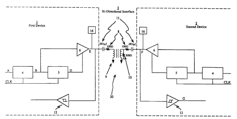
Figure 1 is a block diagram of the transceiver
circuits for each device of the present invention showing
the interconnection between the devices across the
isolation barrier of the interface.
Figure 2 is a detailed circuit diagram of the
present invention showing the use of a pulse transformer as
the isolation barrier.
Figure 3 is a detailed circuit diagram of the
present invention showing the use of a capacitative
coupling as the isolation barrier.
Figure 4 is a timing chart diagram for describing
the operation of the circuits of the present invention.
Figure 5 is a block diagram showing the
implementation of the present invention between the LLC and
PHY chips pursuant to the IEEE P1394 specification.
WO 94/16390 PCT/US93I12324
215 ~~7~
-lo-
The present invention relates to a method and
apparatus for the transmission of data signals across an
interface comprising an isolation barrier disposed between
adjacent devices connected via a bus. In the following
description, numerous details are set forth such as
voltages, currents, device types, etc., in order to provide
a thorough understanding of the present invention. It will
be obvious, however, to one skilled in the art that these
details are not required to practice the present invention.
In other instances, well-known circuits, methods and the
like are not set forth in detail in order to avoid
unnecessarily obscuring the present invention.
With reference to Figs. 1 and 2, the present invention
comprises a first device 1 and a second device 2
interconnected across an interface 3 by means of a bus 20.
The bus 20 comprises at least one transmission line 21 for
transmitting data and control signals and further comprises
an isolation barrier 9 coupled to the transmission lines 21
for electrically isolating the transmitting and receiving
circuitry of the two devices 1 and 2 to prevent ground
loops therebetween. Blocking capacitors 11 of
approximately .OOl~lf are coupled to the transmission lines
WO 94/16390 PC'TIUS93/1232a
215 137 3
-11-
21 of the bus.20 on each side of the isolation barrier 9 to
prevent DC current from being supplied to the isolation
barrier 9. In addition, as shown in Figs. 1 and 2, three
resistors, two series resistors 8 of approximately 10012
and a third shunt resistor 10 of approximately 300f2 (which
is connected to ground to shunt the pulse transformer 9),
are further coupled to the transmission lines 21 of the bus
20. The series resistors 8 are disposed on respective
sides of the isolation barrier 9 to provide signal voltage
attenuation and current limiting in order to protect the
input diodes (not shown) of each device 1 and 2. The shunt
resistor 10 determines the amount of voltage attenuation
and acts to help discharge the pin capacitance of each
device 1 and 2 when their drivers 6 are tri-stated. The
values for the components described above have been chosen
for transmission rates on the bus of approximately 50
Megabits/second so that for different transmission rates,
these values would have to be modified as is well-known in
the art.
According to one embodiment of the present invention,
the interface 3 between the devices is half duplex, bi-
directional such that each device 1 and 2 comprises a
transceiver having a transmitter or driver 6 consisting of
a tri-state gate and a receiver 12 consisting of a Schmidt
WO 94/16390 PCT/US93/123Z
215 ~~a3
-12-
trigger. Furthermore, according to this embodiment, the
isolation barrier 9 comprises a pulse transformer 9 (of 80
~1H) for galvanic isolation of the circuitry of each device
1 and 2 as is well-known in the art. In the following
description, the method and apparatus of the present
invention will be explained in terms of the transmitter 6
of the first device 1 transmitting the transmission signal
to the receiver 12 of the second device 2 where it is
reconstituted into the original data signal input to the
circuitry of the first device 1. Due to the bi-directional
nature of the interface 3, the configuration of elements
and their operation are identical for each device.
However, the present invention is applicable to uni-
directional interfaces 3 and to isolation barriers 9 other
than pulse transformers 9 and capacitative couplings shown
in Fig. 3).
In the first device 1, an NRZ input data signal A
having digital high and low values is generated from a
memory read, a peripheral input device or the like. As
shown in Fig. 1 and more specifically in Fig. 2, this data
signal A is supplied to a data synchronizer 4 consisting of
a first D-Q flip-flop 13 for synchronizing the data signal
A with a clock signal also input to the first D-Q flip flop
13. The synchronized data signal B derived therefrom is
WO 94/16390 PCT/US93/1232.
215 13 7 3
-13-
supplied along with the clock signal to a digital
differentiator 5 for differentiating the pulses of the data
signal A. As shown in Fig. 2, the digital differentiator 5
may comprise a second flip-flop 14 for receiving the
synchronized data signal B and the clock signal and
outputting a delayed data signal C. This delayed data
signal C is next supplied as input along with the
synchronized data signal B to an exclusive OR gate 15.
With reference to the signals B and C shown in the timing
chart of Fig. 3, the exclusive OR gate 15 senses both the
positive and negative transitions of the pulses in the
synchronized data signal B and outputs as the digitally
differentiated signal D a series of pulses corresponding to
these transitions.
Now referring to both Figs. 1 and 2, the synchronized
data signal B is supplied as a first (data) input to a
transmitter 6 or driver 6 consisting of a tri-state gate 6.
The tri-state gate 6 also receives as a second (control)
input the digitally differentiated signal D which enables
the gate 6 when high and disables the gate when low. A
bias voltage 16 is applied to the output of the tri-state
gate 6 to maintain the output of the gate 6 at an
intermediate state of approximately 2.5 volts when the gate
6 is disabled. As shown in Fig. 2, the bias voltage 16 is
WO 94/16390 PCT/US93/1232~
215 1373
-14-
generated by a tied back inverter 16, which in some
instances, may require two pins in order to connect the
input to the output. It is also permissible to set the
bias voltage 16 used in the present invention in other
ways, such as with an external resistor voltage divider
having SKS2 resistors.
When the gate 6 is disabled, a first intermediate
transmission signal E as the output of the gate 6 is driven
on the bus 20 and transmitted across the isolation barrier
9. When the digitally differentiated signal D goes high,
the gate 6 is then enabled, in which case, if the
synchronized data signal B is also high, a first high
transmission signal E as the output of the gate 6 is driven
onto the bus. This first high transmission signal E
comprises a high state of approximately 5 volts. However,
if the gate 6 is enabled and the input synchronized data
signal B goes low, then a first low transmission signal E
is driven onto the bus 20. This first low transmission
signal E comprises a low state of approximately 0 volts.
Therefore, the transmitter circuitry of the first device 1
converts the NRZ input data signal A into a DC balanced
transmission signal E (without increasing the signal's high
frequency bandwidths that can be effectively transmitted
across the isolation barrier 9. As would be obvious to one
WO 94/16390 PCT/US93/1232..
215 ~3~~
-15-
skilled in the art, the foregoing signal amplitudes may
vary (i.e., higher or lower) depending upon the specific
bias voltage 16 utilized and the specifications of the
particular electronic components also used.
When the first transmission signal E is driven onto
the bus, it is received as 0 volt DC input to the pulse
transformer 9. The transformer 9 magnetically couples this
signal to the bus 20 on the opposite side adjacent to the
second device 2 where the output is a second transmission
signal F. As can be seen from the timing chart of Fig. 9,
the second transmission signal F is substantially the same
as the first transmission signal E except that it varies in
amplitude therefrom. This second transmission signal F is
then received as input to a receiver 12 of the second
device 2 consisting of a Schmidt trigger 12. The Schmidt
trigger 12 reconstitutes the non-return to zero data of the
second transmission signal F into the digital pulses of the
synchronized data signal B originally received as input to
the digital differentiator 5.
The Schmidt trigger 12 comprises two threshold
voltages centered around the bias voltage 16, preferably
having the values of 2 volts and 3 volts, where 3 volts is
the threshold for rising edges and 2 volts is the threshold
WO 94/16390 PCT/US93/1232~t
215 1373
-16-
for falling edges which cause the Schmidt trigger 12 to go
high and low, respectively. With reference to the timing
chart of Fig. 9, the output of the Schmidt trigger 12 is
therefore a series of high and low transitions which in
effect reconstitutes the synchronized data signal B.
However, as an alternative to a Schmidt trigger 12, it is
noted that any electronic component can be utilized which
has as an output a high data signal when the voltage of its
input signal reaches a value substantially above the
voltage bias 16, and a low data signal when the input
signal reaches a value substantially below the voltage
bias.
In addition to the foregoing description, another
embodiment of the method and apparatus of the present
invention is designed specifically for implementation with
the multi-speed bus architecture scheme described in IEEE
Standards Document P1394 entitled "High Performance Serial
Bus". This document is appended hereto as Appendix A for
reference. The bus architecture scheme described in P1399
is intended to provide a multi-speed, serial bus 20 having
a low cost, universal interconnection between cards on the
same backplane, cards on other backplanes, and external
peripherals. It also provides for an arbitrary bus topology
where devices or nodes (i.e. addressable devices coupled to
WO 94/16390 PCT/US93112324
2151373
-17-
the bus having a minimum set of control registers) coupled
to the bus 20 need not be arranged in a cyclic network but
can be arbitrarily coupled to other device 5 via the serial
bus 20 to form an assorted number of network arrangements.
In this embodiment, as shown in Fig. 5, the multi-
speed serial bus 20 comprising a twisted pair cable 20 is
provided for universal interconnection between computer
devices arbitrarily configured on the bus. Each device 1
and 2 comprises a physical channel interface chip (or "PHY"
chip) 25 directly connected to the serial bus 20 for
arbitrating, transmitting, receiving and re-timing of the
data signals. Each device similarly comprises a link layer
chip (or "LLC" chip) 29 which transmits and receives the
data signals at a fixed speed to and from the PHY chip 25
and interfaces with the processing intelligence of the
device. The fixed speed transmission between the two chips
29 and 25 is enabled by a conversion process whereby the
bus 20 between the two chips 24 and 25 becomes wider (i.e.
more transmission channels are used) for faster data signal
transmissions. For example, for a 100 I~it transmission,
the bus 20 must be at least two bits wide; for a 200 I~it
transmission, the bus must 20 at least four bits wide; for
a 400 Mbit transmission, the bus 20 must be at least eight
bits wide; and so on. In this embodiment, the interface 3
WO 94116390 PC'T/LJS9311Z324
215 13~ 3
of the present invention comprising the isolation barrier 9
is implemented between the PHY and LLC chips 24 and 25 so
as to permit the development of a universal interconnection
in which a standard serial bus cable 20 can be connected
between the PHY chips 25 of adjacent devices 1 and 2.
In this implementation, the signals transmitted are in
the form of NRZ data signals which require very broad band
transmission capabilities. Due to the fact that a pulse
transformer 9 having a narrow band transmission channel is
implemented as the isolation barrier 9, it is necessary
that the transmitting and receiving circuitry of the PHY
and LLC chips 24 and 25 convert the data signals into
narrow band data signals for transmission between the PHY
and LLC chips 29 and 25. Therefore, according to the
method and apparatus of the present invention, the
circuitry described above is implemented between the PHY
and LLC chips so as to provide a simple method using
digital standard cell or gate array technology in a
standard digital CMOS process to pass the NRZ data signals
across the isolation barrier 9 of the interface 3 disposed
between the two chips 24 and 25.
While the present invention has been described in
conjunction with the above-embodiments, it is evident that
WO 94116390 PCT/US9311232~
_ 215 ~~7~
numerous alternatives, depictions, variations and uses will
be apparent to those skilled in the art in light of the
foregoing description. Specifically, the interface 3 may
be uni-directional or bi-directional and may represent the
communications 'channel between two separate devices 1 and
2, two IC chips 24 and 25 or the like. In addition, the
isolation barrier 9 coupled to the bus in the interface may
comprise a variety of devices or configurations which
electrically isolate the transmitting and receiving
circuitry of the two devices 1 and 2.