Note: Descriptions are shown in the official language in which they were submitted.
21~146~
94/15~2 PCT~S93/1~3
Description
HIGH CONTRAST THIN FILM
ELECTROTTJMTN~SCENT DISPLAY
Technical Field
This invention relates to electroluminescent
display panels and more particularly to high contrast
high specularity electroluminescent display panels.
Backy~uul,d Art
Thin film electroluminescent (TFEL) display panels
offer several advantages over.older display
technologies such as cathode ray tubes (CRTs) and
liquid crystal displays (LCDs). Compared with CRTs,
TFEL display panels require less power, provide a
larger viewing angle, and are much ~h i n~er . Compared
with LCDs, TFEL display panels have a larger viewing
angle, do not require auxiliary lighting, and can have
Fig. 1 shows a conventional TFEL panel 10. The
TFEL panel has a glass panel 11, a plurality of
transparent electrodes 12, a first layer of a
dielectric 13, a phosphor layer 14, a second dielectric
layer 15, and a plurality of metal rear electrodes 16
perpendicular to the transparent electrodes 12. The
transparent electrodes 12 are typically indium-tin
oxide (ITO) and the metal electrodes 16 are typically
Al. The dielectric layers 13,15 to protect the
phosphor layer 14 from excessive dc currents. When an
electrical potential, such as about 200 V, is applied
between the transparent electrodes 12 and the metal
electrodes 16, electrons tunnel from one of the
interfaces between the dielectric layers 13,15 and the
-- 1 --
W094/15~2 PCT~S93/1~3 ~
465
phosphor layer 14 into the phosphor layer where they
are rapidly accelerated. The phosphor layer 14
typically comprises ZnS doped with Mn. Electrons
entering the phosphor layer 14 excite the Mn causing
the Mn to emit photons. The photons pass through the
first dielectric layer 13, the transparent electrodes
12, and the glass panel ll to form a visible image.
Although current TFEL panels are satisfactory for
some applications, more advanced applications require
brighter higher contrast panels, larger panels, and
sunlight viewable panels. One approach in attempt to
provide adequate panel contrast under high ambient
illumination is the use of a circular polarizer filter
which reduces ambient reflected light. A circular
polarizer filter operates best with a TFEL panel which
is very specular. If the specularity of the metal rear
aluminum electrodes 16 can be increased, then the
efficiency of the circular polarizer filter will also
increase.
Disclosure of the Invention
An object of the present invention is to reduce
the reflection of ambient light and enhance the
contrast of a TFEL panel to provide a sunlight viewable
TFEL panel.
2S According to the present invention, the layered
structure of a TFEL panel includes a layer of phosphor
which is deposited using thermal evaporation at a rate
which is at least 50 Angstroms per second to enhance
the specularity of the panel.
According to another aspect of the present
invention, a display system includes an enhanced
specularity TFEL panel and a circular polarizer filter.
-- 2
21~1~6~
~ 094/15~2 PCT~S93112~3
-
When circularly polarized light from the filter
strikes a specular surface the direction of the
polarization (i.e., either clockwise or counter
clockwise) is reversed and this light can no longer
pass back through the linear polarizer plate which is
an integral part of the circular polarizer filter.
Therefore, the greater the specularity of the
electroluminescent panel the less reflected light which
passes back through the circular polarizer ~ilter and
hence the greater the contrast of the display panel.
The enhanced specularity TFEL display of the
present invention provides improved display contrast
and is comfortably viewable in elevated ambient
lighting conditions. These and other objects, features
and advantages of the present invention will become
more apparent in light of the following detailed
description of a preferred embodiment thereof, as
illustrated in the accompanying drawings.
Brief Description of the Drawings
Fig. 1 is an illustration of a partial sectional
view of the layered structure of an AC thin film
electroluminescent (TFEL) panel;
Fig. 2 is an illustration of an enhanced contrast
TFEL display system according to the present invention
including an increased specularity TFEL panel and a
circular polarizer filter;
Fig. 3 is a diagram illustrating ambient light
reflected off a prior art TFEL display panel and a
circular polarizer filter, and light emitted from an
illuminated pixel of the prior art TFEL display panel
all directed towards a viewer; and
Fig. 4 is a diagram illustrating ambient light
W094/15~2 2~S1~ PCT~S93/1~3~
reflected off the increased specularity display panel
and the circular polarizer filter both of Fig. 2, and
light emitted from an illuminated pixel of the
increased specularity panel all directed towards the
s viewer.
Best Mode For Carrying Out The Invention
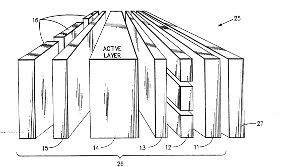
Referring to Fig. 2, a display system 25 according
to the present invention includes a highly specular AC
driven thin film electroluminescent (TFEL) panel 26 and
a circular polarizer filter 27. The filter 27 has a
transmission of 30%-40~, preferably about 37%, and an
anti-reflection coating ~hich provides about a 0.2%
reflectivity. As known, a circular polarizer filter
typically includes a linear polarizer and a quarter
wave plate such that non-polarized light is first
linearly polarized by the linear polarizer and then
input to the quarter wave plate which circularly
polarizes the light.
The layered structure of the highly specular panel
26 and the panel lO of Fig. l are essentially the same
and therefore similar layers will retain the same
numerical designation.
The first step in making a TFEL panel 26 like the
one shown in Fig. 2 is to deposit a layer of a
transparent conductor on a suitable glass panel ll.
The glass panel ll can be any high temperature glass
that can withstand the phosphor anneal step described
below. For example, the glass panel can be a
borosilicate glass such as Corning 7059 (Corning
Glassworks, Corning, NY). The transparent conductor
can be any suitable material that is electrically
conductive and has a sufficient optical transmittance
~ 094l15~2 21 5 1 ~ ~ ~ PCT~S931~33
for a desired application. For example, the
transparent conductor can be ITO, a transition metal
semiconductor that comprises about 10 mole percent In,
is electrically conductive, and has an optical
transmittance of about 85% at a thicknesc o~ about 200
nm. The transparent conductor can be any suitable
thickness that completely covers the glass and provides
the desired conductivity. Glass panels on which a
suitable ITO layer has already been deposited can be
purchased from Donnelly Corporation (Holland, MI). The
remainder of the procedure for making a TFEL display of
the present invention will be described in the context
of using ITO for the transparent electrodes 12. One
skilled in the art will recognize that the procedure
for a different transparent conductor would be similar.
ITO electrodes 12 can be formed in the ITO layer
by a conventional etch-back method or any other
suitable method. For example, parts of the ITO layer
that will become the ITO electrodes 12 can be cleaned
and covered with an etchant-resistant mask. The
etchant-resistant mask can be made by applying a
suitable photoresist chemical to the ITO layer,
exposing the photoresist chemical to an appropriate
wavelength of light, and developing the photoresist
chemical. A photoresist chemical that contains 2-
ethoxyethyl acetate, n-butyl acetate, xylene, and xylol
as primary ingredients is compatible with the present
invention. One such photoresist chemical is AZ 4210
Photoresist (Hoechst Celanese Corp., Somerville, NJ).
AZ Developer (Hoechst Celanese Corp., Somerville, NJ)
is a proprietary developer compatible with AZ 4210
Photoresist. Other commercially available photoresist
chemicals and developers also may be compatible with
wo94/1~2 ~5~ PCT~S93/12~3
the present invention. Unmasked parts of the ITO are
removed with a suitable etchant to form ch~nnels in the
ITO layer that define sides of the ITO electrodes 12.
The etchant should be capable of removing unmasked ITO
without damaging the masked ITO or glass 11 under the
lln~kP~ ITO. A suitable ITO étchant can be made by
mixing about 1000 ml H20, about 2000 ml HCl, and about
370 g anhydrous FeCl3. This etchant is particularly
effective when used at about 55 C. The time needed to
remove the unmasked ITO depends on the thickness of the
ITO layer. For example, a 300 nm thick layer of ITO
can be removed in about 2 minutes. The sides of the
ITO electrodes 12 should~be chamfered, as shown in the
figures, to ensure that the first dielectric layer 14
can adequately cover the ITO electrodes. The size and
spacing of the ITO electrodes 12 depend on the
dimensions of the TFEL display. For example, a typical
12.7 cm (5 in) high by 17.8 cm (7 in) wide display can
have ITO electro~es 12 that are about 30 nm thick,
about 250 ~m (10 mils) wide, and spaced about 125 ~m (5
mils) apart. After etching, the etchant-resistant mask
is removed with a suitable stripper, such as one that
contains tetraméthylammonium hydroxide. AZ 400T
Photoresist Stripper (Hoechst Celanese Corp.) is a
commercially available product compatible with the AZ
4210 Photoresist. Other commercially available
strippers also may be compatible with the present
invention.
The dielectric layers 13,15 can be deposited by
any suitable conventional method, including sputtering
or thermal evaporation. The two dielectric layers
13,15 can be any suitable thickness, such as about 80
nm to about 250 nm thick, and can comprise any
- 6 -
~ 094/15~2 215 1~ ~ ~ PCT~S93112~3
dielectric capable of acting as a capacitor to protect
the phosphor layer 14 from ~Y~s~ive currents.
Preferably, the dielectric layers 13,15 will be about
200 nm thick and will comprise SiO~. The phosphor layer
14 can be any conventional TFEL phosphor, such as ZnS
doped with less than about 1% Mn. According to the
present invention the phosphor layer is deposited at a
rate which is at least 50 ~,~L oms per reco~ (e.g.,
50-100 Angstroms/sec) in order to provide a smoother
layer which enhances the specularity of the panel 26.
The phosphor layer 14 can be about 5000-8000 Angstroms
thick (i.e., 500-800 nm), and preferably about 5000
Angstroms deposited at a rate of 50 Angstroms/second.
After depositing the phosphor layer 14 followed by
the second dielectric layer 15, the panel should be
heated to about 500-C for about 1 hour to anneal the
phosphor. Annealing causes Mn atoms to migrate to Zn
sites in the ZnS lattice from which they can emit
photons when excited.
After Anne~ling the phosphor layer 14, the metal
electrodes 16 are formed on the second dielectric layer
15 by any suitable method, including etch-back or lift-
off. The metal electrodes 16 can be made from any
highly conductive metal, such as Al. As with the IT0
electrodes 12, the size and spacing of the metal
electrodes 16 depend on the dimensions of the display.
For example, a typical 12.7 cm (5 in) high by 17.8 cm
(7 in) wide TFEL display can have metal electrodes 16
that are about 100 nm thick, about 250 ~m (10 mils)
wide, and spaced about 125 ~m (5 mils) apart. The
metal electrodes 16 should be perpendicular to the IT0
electrodes 12 to form a grid.
_ The present invention is based on the fact that
-- 7 --
WO94/15~2 ~ 6~ PCT~S93/12W
when circularly polarized light strikes a specular
surface, the direction of the circular polarization
(i.e., either clockwise or counter clockwise) is
reversed and this light can no ~onger pass back through
the linear polarizer plate which is an integral part of
a circular polarizer filter. Therefore, the amount of
ambient light incident on the surface of the panel
which reflects back to the observer can be reduced with
a highly specular TFEL panel and a circular polarizer
filter. Increasing the specularity of the panel
increases the efficiency of the circular polarizer
filter and results in improved display contrast since
less ambient light is reflected. An example of the
improvement in contrast provided by the present
invention over the prior art is now in order.
Fig. 3 is a functional illustration of a
conventional prior art TFEL display system 30 within an
ambient light environment of 2,000 foot-candles (fc) of
light. Ambient light 32 strikes the circular polarizer
filter 27 at a thirty degree angle taken from a line
normal to the plane of the face of the filter 27
resulting in four foot-lamberts (fl) of light 34 being
reflected off the face of the filter 27. The ambient
light 32 is also reflected off a conventional TFEL
panel 35 resulting in about forty-two fl of light 36
being reflected towards the viewer 38. The TFEL panel
35 also provides about 50 fl of light emitted from an
illuminated pixel. However, due to the 37%
transmission of the filter only about 18.5 fl of light
40 is emitted from the display system 25.
Contrast is the measure the panel's the reflected
light 34,36 compared to the emitted light 40, and
-- 8
94/15~2 21 514 6 ~ P~T~S93112~3
contrast is defined as:
Contrast = Panel emitted light + ambient reflected light
ambient reflected light 1 ]
Since the panel emitted light is 18.5 fl, and the
reflected light components from the filter and panel are
4 fl and 42 fl respectively, the contrast of the prior
art panel 25 is:
Prior art panel contrast = 18.5 + 42 +4 ~EQ.2]
42 + 4
~ = 1.4
Fig. 4 illustrates an enhanced display system 25 of
the present invention having the highly specular TFEL
panel 26 and the circular polarizer filter 27. Note,
the display system of Fig. 4 is substantially the same
as the display system in Fig. 3 and therefore where ever
possible elements which are essentially the same will
retain the same numerical designation. The high
specular panel 26 has an active area of 3.5" x 4.7" with
320 ITO column electrodes each 2000 angstroms thick and
sputter deposited, and 240 Al row electrodes each 1500
angstroms thick and deposited by thermal evaporation.
The phosphor layer is 8000 angstroms thick and deposited
by thermal evaporation at a rate of 50 angstroms per
second. The dielectric layers were each RF sputtered
2000 angstroms thick SiON. The display system 25 is
within an ambient lighting environment of 2000 fc, which
results in four fl of reflected light 34 off the filter
27 front surface. The ambient light 32 is also
reflected off the highly specular TFEL panel 26 with a
_ g _
_ PCT~S93/1~3
net result that only 4.4 fl of reflected light 42 passes
through the circular polarizer filter. Attention is
drawn to the fact that the reflected light 36 (Fig. 3)
from the prior art TFEL panel 35 was 42 fl in comparison
to only 4.4 fl of reflected light 42 (Fig. 4) from the
highly specular TFEL panel 26 of the present invention.
As a result, substituting the numbers associated with
the enhanced display system 25 into Eq. 1 results in a
display contrast of:
enhanced specularity = 18.5 + 4 + 4.4
panel contrast ~EQ~3~ 4 4
= 3.2
Therefore, the present invention provides about a
2-to-1 improvement in contrast over the conventional
specular display panel of Fig. 3. In addition since the
TFEL display panel of the present invention has
increased specularity it exhibits a diffuse reflectance
on the order of only 2%, whereas the prior art panels
exhibit diffuse reflectance of 15-20~.
The contrast improvement associated with the
enhanced display system 25 is primarily due to the
improvement in the specularity of the TFEL panel 26 and
the resulting increase in efficiency which the circular
polarizer filter provides. ~nh~ncing the specularity of
the TFEL panel 26 increases the efficiency of the
circular polarizer filter 27 and results in improved
display contrast since less light is reflected.
Incidently it will be appreciated that if the
display system of the present invention will be used
outside for prolonged periods, an ultraviolet (W)
filter should be placed in front of the circular
-- 10 --
~ 094/15442 21~14 6 ~ ~CT~S93/12233
polarizer 27 to ensure that W light does not destroy
the polarizing properties of the circular filter.
Although the invention has been shown and described
with respect to a preferred embodiment thereof, it
should be understood by those skilled in the art that
various other changes, omissions, and additions may be
made to the embodiments disclosed herein, without
departing from the spirit and scope of the present
invention.
We claim:
-- 11 --