Note: Descriptions are shown in the official language in which they were submitted.
W4 94I"i412b . , ~CT~13J11343
.1!
DESCf~IPTION
FAULT TOI.i»RANT MUkTIPOIIWT DATA COLLECTION SYSTEM
Technical Field
This invention relates to systems which collect data from multiple
sensors, particularly accelerometers installed at various points around a
manufacturing site, and bring the data to a central monitoring location.
It is particularly related to systems where the sensors are uniquely
addressable over a common data bus.
Background Art
Production line and process machinery needs to be monitored
for wear to avoid expensive, unexpected breakdowns. This is often
done with accelerometers installed on the bearings of motors, pumps
and her critical machinery to monitor the vibration of the equipment.
Breakdowns are often preceded by changes in the equipment vibration
level. These changes can be detected through regular monitoring,
allowing the equipment to be repaired during regularly scheduled
maintenance periods.
One method of monitoring the sensors is for maintenance
personnel to take regular readings of the vibration levels at the sensors
by Carrying a portable data storage unit directly to each sensor to collect
the data. This is time consuming, but effective.
Another method is for the sensors to be individually hard-wired
to a central station. In this arrangement, a separate wire pair runs from
each sensor to the central monitoring station or to a multiplexer which
is then connected to the central station. This design simplifies the data
collecti~ task by allowing the data to be collected from the central
station mounted in a canvenient location.
In the central monitoring station design, other types of sensors,
such as tachometers, pressure sensors, temperature senses and the like
may also be added to the system. This allows production process
monitcxing to be integrated into the vibration monitoring system.
wo ~ar~l~i~ d'~ r~crnrr~~~i
- _2_
In large systems, however, the numerous sensors makes the cost
of running individual wire pairs from the sensors to the central location
or multiplexer a major facto in the total, cost of the system. Moreover,
vibration sensors used to detect abn'~inal vibrations caused by wear,
usually need to be monitored oi~,ly briefly at widely scattered time
intervals. Thus, prior art systems with a single wire pair running to each
senses has far more data transmitting capacity than is required for the
majority of applications. A single data bus shared by the sensors is
therefore desirable to reduce cabling cost and complexity.
Although the technique of using a common data bus for
connecting to digitally addressable electronic elements is known, it has
certain difficulties in a factory environment when implemented for
monitoring sensors. One is that all the data from all the senscxs passes
over a single data bus. In the real world, with a network of sensors
spread throughout a factory environment, a single data bus is
susceptible to damage. An open circuit on the bus will cause the loss of
information from all sensors beyond the open circuit and a short circuit
makes communication impossible with any sensor on the bus.
Moreover, if the sensors are powered over the cable, the power
transmission capabilities of the cable become a factor. Accelerometers
are powered through the data bus wires over which the data is
transmitted. Reasonably sized data bus wires do not have the power
carrying rapacity to continuously and simultaneously power the large
number of sensors desired for many installations.
A further difficulty in a bus configuration design is that the
sensors need to be uniquely identified by an address so that a desired
sensor on the bus can be singled out and told to transmit its information.
A digital address and digital address circuitry is cle~ly the most suitable
for this task, but commonly available sensors generate analog data. This
requires the use of one pair of wires for addressing the sensors and
another set for transmitting the analog data. An alternative solution is to
convert the analog data to digital form and run an all digital bus, but this
requires expensive analog to digital circuitry at each sensor. Neither
solution is desirable.
2 ~t 5I 5 0 ~ ~r~~><
~ . .3-
Accordingly, one object of the present inv~eration is to provide a
bused data collection system wherein the system includes redundant
p~allel data buses for fault tolerance in the event that any one bus is
damaged.
Another object of the invention is to provide a design in which
each sensor is connected to several data buses, and a central controller
can electrically switch any sensor onto any selected one of the data
buses.
A further object of the invention is to provide a design in which
multiple parallel data buses may be simultaneously used to receive data
from different sensors to permit real time direct comparison between the
output of the sensors.
Still another object of the invention is to provide a design in
which digital sensor addressing and analog data transmission occur on a
shared data bus,
Another object of the invention is to provide a des#gn in which
multiple sensors shaue a single data bus, and that data bus is used
bidi~ectionally to transmit digital address data from the central location
to select a specific one of the sensors and to transmit analog senses data
from the sensor to the central location,
Still other objects and advantages of the invention will in part be
obvious and will in part be apparent from the specification.
Disclosure of Invention
The invention achieves fault tolerant multipoint data collection
through the use of a set of redundant parallel two-wire data buses
organized into a single cable. A central controller is connected to a
plurality of senses through the cable which connects to a
corresponding plurality of addressable sensor interfaces positioned
between the cable and the sensor interface. The central controller
generates an address signal identifying a selected sensor interface and a
selected data bus, and sends that signal through bus interfaces, one for
each data bus, connected between the controller and the corresponding
data bus.
Each sensor interface is connected to all the data buses in the
cable and includes a means responsive to the central controller signal
far recognizing its unique address in the signal and connecting its
corresponding sensor to a selected one of the data buses specified in the
signal.
The adc~ess signal is composed of a sensor address portion and a
bus address portiob. This permits the central controller to specify any
sensor and any one of the data buses by transmitting the central
controller signal over any one of the data buses.
The invention uses a particularly advantageous method of sharing
a single data bus for digital address signals, sensor power and analog
data from the sensor. This eliminates the need for a separate digital
address bus. In the simplest form of the invention, a single data bus is
shared for digital and analog data, but in the preferred design, the
benefits of the shared bus are multiplied through the use of multiple
parallel buses which provide redundancy for fault-tolerant operation.
The central controller supplies power to the sensors from a sensor
power supply means through the selected data bus. The sensor power
means provides power to the sensor, and the sensor uses that power to
generate analog data within a carefully controlled and restricted voltage
range having a preset upper and lower voltage limit.
The controller signal used to select the data bus and the desired
sensor is a digital signal; generated by a bus inderface, having an on
voltage greater than the maximum sensor power voltage and an off
voltage which is less than the minimum voltage. This places the
controller signal completely outside of the voltage range available for
data and permits the sensor interfaces to disaiminate between the two
on the basis of this difference.
In the preferred design, the central controller encodes the sensor
and bus address using a self-clocking format in which each data bit of
the address is delivered asynchronously and is preceded by a clock bit.
This makes the system insensitive to random propagation delays
incurred through long cable lengths connecting distant sensors to the
controller.
The sensor interface includes a circuit means for disconnecting
the sensor from the selected data bus whenever sensor power is
removed from the data bus.
~irr
wo yen
-5-
Brief D,e~cri~~ion of the Clrawin~
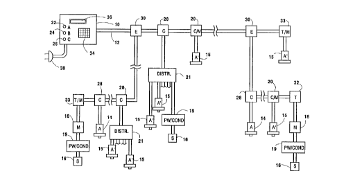
Fig. 1 illustrates the bus layout of the monitoring system.
Fig. 2 is a circuit diagram in block diagram form showing the
central cnntroiler.
Fig. 3 is a circuit diagram of a bus interface in the central
controller as shown in block form in Fig. 2 .
Fig. 4 is a circuit diagram of a sensor interface.
Fig. 5a is a graph of voltage versus time showing the tranarnission
of a digital address signal on a data bus followed by receipt of analog
data from the selected sensor on the same bus.
Fig. 5b is a 8raph of voltage versus time showing the p~uises
generated by address detector circuitry and used to read the self clocked
data in the address signal.
Fig. 6 is a circuit diagram of bias~mpedance converter circuitry
suitable for use with the accelerometers.
Modes for CacrYina 4~ui the inventifln
Referring to Fig. 1, the invention comprises a central controller
10 connected via a cable 12 to multiple specialized accelerometers 74
(mark- v A), generic accelerometers 15 (marked A') and generic sensors
1b (marked S). The central controller would normally be installed in a
convenient location where data from the sensors may be collected. It
accepts input specifying a sensor to be monitored, signals the sensor to
connect to a data bus within cable 12, provides power to the sensors
and associated address circuitry over the cable and provides the data at
an output.
The sensors 14, i 5 and 16 are caonnected to the buses within
cable 12 through sensor interfaces, described in ccuonec~ion with Fig. 4.
The sensors are typically scattered throughout a manufacturing facility
mounted at various critical monitoring points. By way of example,
accelerometers are often mounted in vibrationai contact with the
bearings of rotating machinery.
Each sensor has its own sensor interface which stores a unique
address, permitting the central controller to specify particular sensors via
the address of the corresponding sensor interface. In specialized sensor
type 14, which in the preferred design includes some or all of the
CVO 9r41i46~i FG"x/U~3n1343
accelerometers, the sensor interface is located within the case housing
the sensor. This provides a convenient one piece assembly, particularly
for accelerometers which comprise the majority of the sensors in many
installations.
The generic sensors 16 can be any orie of a wide variety of off
the-shelf sensors which are availabl~~to measure pressbre, temperature,
speed, strain, flow rate, or any other desired physical parameter. Such
sensors do not have the desired integal sensor interface, so it is
provided separately. Generic accelerometers 15, which also tads the
sensor interface may also be used with the system with the advantage
that existing vibration monitoring systems may be upgraded without the
necessity of replacing all the accelerometers.
For sensors without the integral sensor interface, the interface
may be located at any one of a number of suitable locations as shown in
Fig. 1. One such location is within a module 18 (marked M) dedicated
to the sensor interface function. A power and signal conditioner 19
(marked PW/COND) is also shown positioned between the sensor and
the interface module. Its function is to provide any specialized power
that the sen~r 16 may need and to convert the sensor's output signal to
a form rnmpatible with the monitoring system. The operation of power
and signal conditioner 19 depends upon the individual re~puirements of
the particul~ sensor attached to it, so it is not described in dc~ail, but it
produces an analog output signal similar within the same voltage range
as the accelerometer output signal described below.
Accelerometer types 14 and 15, and many neric sensors can
be supplied with power over cable 12 from power sources within, or
oon~ected to, the central controller 10. However, some specialized
sensors are powered more conveniently from power sources within the
power conditioners 19 which may need separate connexion to external
power sources.
Other suitable locations for the module containing the sensor
interface are within the connector 20 (marked C/M) making connection
to the cable 12, within a terminator connector 33 (marked T/M) or
within a multiple sensor distribution box 21 (marked DlSTR.). The
rnuitiple sensor distribution box is connected to the cable 12 with a
WO 9~ri4~26
1 ~ ~ J~ ~ ~ r~lrririi3
single connector 28; but contains several sensor interfs, each with its
own unique address, and each corresponding to one of multiple sensors
connected to it.
Regardless of where the senses interface is installed, the sensor is
ultimately connected to the cable 12 through 'the sensor interface via a
rnnnector which may take the form of a standard connector 28 (marked
C); a connector with integral senses interface 20 (marked C/M), a
terminator 32 (marked T) or a terminate with integral sensor interface
33 (marked T/lvu.
The connector makes connection to wire hairs within the cable
12 which act as multiple parallel buses to carry power and data to and
from the sensors. The preferred design for the system uses a cable 12
with an internal ribbon cable folded within a round outer sheath. The
sheath may be opened at perforated junctions spaced along its length to
expose the ribbon cable which is then unfolded to a normally flat shape.
Connection to the flattened ribbon cable is made with standard
insulation displacement connectors (IDC), the socket portion of which is
attached to the flattened ribbon cable and the plug portion of vuhich is
attached to the sensor interface. This arrangement permits the sensors to
be quickly attached to the cable at any location along its length and
repositioned or replaced as necessary.
The IDC connectors make contact with the wire pairs in cable
12, without interrupting them. Any connector capable of making such a
connection to the wires in the cable, and any cable configuration
containing multiple accessible wires would also be suitable. The
connectors 28 may be provided with impedance matching circuitry, if
necessary, in accordance with conventional bus design techniques.
Extension connectors 30 (marked E) provide a means of
branching the cable 12. They are similar to the connectors 28 in that
they are also IDGbased connections, but they connect a ixanch of the
cable 12; containing multiple additional sensors along its length, instead
of a single sensor. Terminator connectors 32 (marked T) are similar, but
include a standard resistive termination network to prevent ringing on
the bus.
'WO l~tJ'~ ~~ ~'
P'~»'~IVSl3/11343
_ ~
In the pre~red design Shown, the ri#~bon cable inside cable 12
includes three parallel wire pairs referenced externally as data buses A,
B and C. Those familiar with the art will recognize that more than three
or as few as one data bus may be used to increase or decease the fault '
tolerance of the data collection system. Even a~single data bus design
has advantages over direct wired prior art ~~lata collection systems by '
virtue of the fewer wires it employs.
Referring to Fig. 2, the data bus wire pair for data bus A includes
a signal wire 42 and a cd~responding ground wire 43: The data bus wire
pairs for data buses B and C include signal wires 44 and 46 and ground
wires 45 and 47. As described below the data buses A, B and C are
referenced by the controller 10 digitally in a bus address portion of an
address signal.
The data buses A, B and C are connected to data outputs 22, 24
i 5 and 26 on the central controller 10 through corresponding bus
interfaces 48, 50 and 52 (see Fig. 2). These outputs ere provided so that
a portable data storage unit may be connected to any one of them to
receive data from a selected senses over the corresponding data bus.
in the preferred design, the cable 12 also includes at least one,
and preferably two, additional wire pairs arranged as keep-alive power
buses, to power the sensor interfaces. They supply power to operate the
digital address circuitry in the sensor interfaces so that they can
recognize their address when selected and connect their sense to the
data bus. The sensor itself is not powered ova the keep-alive power
bus, but, instead, is powered over the selected data bus.
The address circuitry in each sensor interface simultaneously
rnonitas all of the data buses. The central controller 10 specifies an
interface and a data bus via an address signal containing the address of
the desired interface and the bus to be used. This~signal is sent to a bus
interface where it is formatted and placed on a data bus. Each sensor
interface receives the signal, and the sensor interface whose internally
stored address matches the address in the signal connects its sensor to
the data bus specified in the bus portion of the address signal so that
data transmission can begin. ,
v~o ~tr>L~ts
.g_
The acid~ess circuitry requires very Ilttle power compared to the
sensor, and a large number of sensor interfaces rnay be simultaneously
powered on the keep,alive bus. The second keep-alive power bus may
be used as a spare, or, where the number of sensors is so large that the
power transmission capability of one keep-alive power bus is exceeded,
the sensors may be split between the two buses.
The controller is powered via a standard AC power connection
38 and includes an input means 34, used to tell the controller what
sensor is to be activated and which data bus should be used to send the
7 0 data from that sensor. For manual operation, the input may be a keypad
34, as shown in Fig. 1 or a keyboard. These allow a sensor address to
be entered manually as well as the desired bus.
Alternatively, the system may be set up for more automated
operation under the external control of a computer or an automated
7 S data storage unit in which case an RS-232 serial interface or a direct
connection to a computer bus may be used as the input. These inputs
may be used instead of, or in addition to, a keypad or keyboard. in
each case, the principal function of the input means is to specify the
address of a senscx to be powered up for' data col lection and a bus over
20 which the data is to be transmitted.
The central controller also includes an output means for signaling
the status of the aantroller. This may take the form of an LCD display
36, as shown in Fig. t . It may also include an RS-232 serial interface, a
computer monitor, a connection to a computer bus or any combination
25 thereof. The output is used to supply information either directly to a
user of the system or to an automated data collector. The information
may include such items as the address of the currently selected sensor,
which of the data buses are in use , whether data is arriving on the buses
and whether the data is good and is not being distorted through
30 clipping.
Referring to Fig. 2, a miaocontroller 40 performs the job of
rnan~aging system operation and translating between the input and
output means 34, 36 on the one hand and the data collection system on
the other. It performs such functions as accepting data from the keypad
35 when keys have been pressed, interpreting the input specifying the
wo n~rc ~c~rrt~~ni~
_10-
~151'~t
sense and bus; preparing a digital address signal, t~xning on certain
trigger signals to activate portions of the bus interface, monitoring to see
if arriving data is gad, sending status information out the output and
other timing and sequencing functions to coordinate the system '
operation.
An optional digital input/output means such as the itS-232 '
connection 37 may be used instead of or in addition to the inputloutput
means 34, 36 to permit automated control of the system from a
computer or portable data logger.
As those familiar with conventional miaocontraller circuits will
recognize, the miarocontroller will also include additional support chips
(not shown), such as buffers, a programmable read only memory
(PROM) to store an inputloutput program which controls the
miaocontroller operation, and a random access memory (RAM) which
may be part of the mitxocontroiler chip or separate. All of these support
chips would be contained within the control section 41 of the central
controller 10, and the design of the microoontroller based control
section 41 is entirety conventional.
The data from the specified sensor gives at the central controller
over one of the specified two-wire data buses 42-43, 44-45 and 46-47;
and is made ex~ernaily available for recording by a data logger or other
device at data outputs 22, 24 and 26. The data buses are connected to
the central controller through three substantially identical bus interfaces
48, 50 and 52.
The microccantr~ler 4Q controls operation of the bus int~rf~uces
over control buses 58, 60 and 62. The control buses include multiple
control and status lines, described fully in connection with Fig,. 3, for
sending and receiving digital signals to and from the bus interfaces.
In addition to the six wires of the three data buses, the cable 12
includes two wires of the keep-alive power bus 54, 55 driven by the DC
power supply 56. The DC power supply also powers the
miarocontroller 40, the bus interfaces 48, 50, 52 and through them, the
sensors over the data buses. Additional two wire data buses and/or
keep-alive power buses may be incorporated into the cable 12 to
provide additional data and/or power pathways.
-11-
The DC power supply 56 dates at least three distinct wolta~ges
to pc~~r different portions of the circuitry, +KPV, +SPV and +DPV.
Power line 57 is shown to emphasize the fact that power is sent to the
bus interfaces and from there to the sensors over cable 12. Other parts
of the central controller are also powered irt a conventional fashion
although the power connections are not shown.
The highest voltage supplied by DC pa~wer supply 56 is the keep-
alive power voltage (+KPV). This is the voltage supplied to the ad~ess
circuitry over the keep.alive bus 54-55. As descxibecl below, this
voltage is also used as the binary "on" voltage in the digital address
signal sent over the data buses. The off voltage is essentially zero volts.
The second, and next lower voltage is sensor power voltage
(+SPV). This voltage is used to supply the constant current sensor
power source 86. The sensors set up a bias voltage that is less than
+SPV on the data buses, with the AC analog data fluctuating mound the
bias voltage. The analog data voltage can never exceed +SPV, and this
difference is used to prevent analog data from being confused with
digital data which is always 0 or +SPV. Re~rictions on the minimum
voltage level of the analog data makes the voltage ranges for valid digital
data and valid analog data mutually exclusive.
The last, and lowest voltage lerei is digital voltage
(+DPV). This voltage is used to power many of the digital integrated
circuits.
Turning nawv to the bus interfaces, Fig. 3 provides a detailed
circuit diagram for bus interface 48 c~necked to data bus A. As the
three bus interfaces 48, 50 and 52 are identical; only bus interface 48
will be fully described.
Digital control signals from the microcontro#Iaer 40 are sent to the
bus interface 48 over various control lines marked "A ADDR" 68, "A
ADDR ON" 70, "A OFF" 72, and "A AUX ON" 74. Digital status signals
from the bus interface are sent to the miaocontroller 40 over status lines
marked "A DATA" 76 and "A CLIP"' 78. The line marked "A AUX" 80 is
an auxiliary DC connection to the sensors over the data bus 42. It may
be used to supply power over the data bus to any sensor that may
require non-standard power, or it may be used for DC data output.
W~4'D~/i!B P'CTIK1S93/113~13
. 21~~,5~2
-~ a-
Genially; however, AC data output is provided at data output
22 from data bus 42 through a conventional AC output network
composed of resistor 64 and capacitor 66. They transmit the AC data
signal and block the DC bias on the data bus during the interval when '
data is being transmitted.
The control and status lines reared tc~ herein are part of the '
control bus 58 on Fig. 2, and the labeled control and status lines 68-$0
in Fig. 3 terminate at addressable inputs and oartputs of the
miaocontroller 40. The miaocontroller 40 also includes
corresponding control and status lines for the other two bus interfaces
50 and 52 within the control buses 60, 62.
The bus interface 48 performs the following exsential functions:
1. It receives a digital address signal from the miaocontroller 40
specifying a sensor address and a data bus, formats the address signal by
shifting its voltage from conventional zero to five volt TTL voltage levels
to zero to +KPV levels to enable the sensor interfaces to recognize it as
a digital address, and then transmits the signal over the data bus 42-43.
.2. It times a delay period during which the address signal is sent,
then applies a constant current power to the data bus 42 in order to set
up the bias voltage and power the selected accelerometer sensor.
3. As data begins to arrive on the data bus 42, the bus interface 48
monitors and tests that data and signals the micxocontroller a) that data
is now arriving and b) that the data is within the operating range.
4. At a subsequent point in time; upon command from the
microeontroller, the bus interface disconnects power from the data bus
42 which resets all the sensor interfaces to a standby mode in which
they await a new address signal.
These functions are principally performed by a timer circuit 82,
an address circuit 84, a sensor power supply 86 and two t2) data
monitoring circuits a8 and 90.
The first step in a data collection cycle is for the mia~ocontroller
to insure that the sensor power is turner! off on the data line 42 by
switching the A OFF line 72 low. This clears flip-flop 92 and opens FET
electronic switch 94 which is connected to the flip-flop 92 over line 96.
wo ~n~6 _ ~ ~. ~ ~, ~ ~ ~ r~crruss~n
-13-
Clearing the flip-flop output opens switch 94 end disconnects the senses
power supply 86 address bus 42.
When the sensor power is ren'toved frorra data bus A, any
' pre~riously selected sensor that is connected to and drawing sensor
power from that data bus will disconnect, reset and switch to the
' standby state.
Next, with tile data bus clear, the microcontro~ler 40 s3g~als the
bus interface that an address is to be sent over data bus A by turning the
A A~DR ON line 70 high.
TO Turning ifne 70 high closes FET switch 98, connecting the .
address circuit 84 to the data bus 42 and simultaneously starts the
timing cycle of timer circuit 82.
Timer circuit 82 will then begin to count out a preset timer
period via a 555 timer 100, as set by the RC time constant of resistor
108 and capacitor 712. At the end of he preset time period, the output
of timer 1 ~ will flip the state of )-K flip-flop 92, closing switch 94 and
supplying sensor power from the sensor power circuit 86 to the data bus
42.
Within the preset time period generated by tirtmr 100, the
micxacontroller 40 needs to generate an address signal specifying the
desired sensor, and send that signal to the bus interface so that the
appropriate sensor can be connected to data bus 42 to receive the
power. In the preferred design, timer 700 generates a delay of at least
700 milliseconds after the A ADDR ON line 70 goes high before it
switches the state of )-K flip-flop 92.
Once the A ADDR ON line 70 is turned high, the address signal
is sent from the micxocontroller 40 to the address circuit 84 over control
line 68. The address signal generated by the microcontroller includes
two portions. The first portion is the address of the sensor interface
connected to the sensor from which data is to be collected.
The second portion identifies the bus over which the data is to be
sent. The A bus interface 48 will be used to signal to a sensor that data
should be transmitted over the A data bus 42.43, the B bus interface 50
will be used to signal to a sensor that data should be transmitted over
the 13 data bus, etc.
wo ~tt~a~s pcrrtri
2151502
The address circuit 64 is basically a voltage level shifter,
converting the address signal generated by the microcontrolier 40 from
its original zero (ofd to five volt (on) levels to a zero (off) to +KPV (on)
digital address signal before it is sent on to the data bis 42.
When timer 100 times out, it clpens syvitch 98 and flips the state
of flipflop 92 closing switch 94 thereby disconnecting the address
circuit 84 from the data bus and connecting instead sensor power
supply 86.
Sensor power supply circuit B6 includes a three terminal power
regulator 102 configured as a constant current source by resistors 104
and 106. Because the power supply is powered with a maximum
voltage of +SPV which is less than +KPV, the analog sensor data
voltage cannot exceed +SPV and cannot be confused with digital
address signals which are either off or +KPV in magnitude.
Biasfmpedance converter circuitry at the accelerometer (see Fig.
6) sets up a nominal bias voltage of SO°k of +SPV from the current
supplied by the sensor power circuit 86. This circuitry also limits the
minimum voltage of the data from the sensor which prevents the
address circuitry on other sensor interfaces from confusing data with
address signals from the miaocontroiler 40. The absence of bias
voltage when the sensor power circuit 86 is disconnected by switch 94
can be uniquely detected in the sensor interface to reset the selected
sensor and take it off line.
The constant current so~ce is particularly suited for powering
erometers. For other types of sensors requiring different forms of
power, the A AUX line 80 maybe used to supply power, provided that
it is limited to the voltage range of minimum data voltage to +SPV as
previously described. The connection of the A AUX line is controlled
over the A AUX ON line 74 by the microcontroller.
The address circuitry 84 shifts the voltage level of the incoming
address bits on A ADDR line 68 so that a digital "an" is +KPV. The
address pulses from line 68 switch transistor 176. When the A ADDR
tine goes high, transistor 116 conducts, the voltage at the collector of
transistor 716 shifts low, which drops the voltage at the inverting input
of comparata 17 8 below the voltage set by the biasing resistors on the
2~.~i~o
,~o ~z.
_15.
non-inverting input of 118 causing tl~e output of i 18 at switch 98 to
shift high to approximately the full +ICPV voltage.
If the sensor interface, to be desaibeci below, is operating
properly, the sensor interface corresponding to the address specified in
the address siginal just transmitted will have connected its sensor to the
A data bus and the biasing circuitry thereon will have set up a bias
voltage on the A data bus of approximately 50% of +SPV. Analog data
ranging between the minimum data voltage and +SPV will begin to
appear on data bus A as the sensor operates, and this data passes to data
output A through capacitor 66.
To verify that good data is arriving, the ~rolt~a~e on data bus A is
monitored by modules 88 and 90. Module 88 monitors the DC bias
voltage, and module 90 monitors the AC voltage to verify that the signal
is in the valid range and is not being dist~ted as a result of clipping or
saturation.
Module 88 monitors the A data bus sisal line over wire 136
through resistor 150, which with capacitor 151 and resistor 149 acts as
a low pass filter and essentially shorts the AC component to ground.
Comparatars 138 and 140 set up a voltage window mound the expected
bias voltage and signal the central controller 40 by turning the A DATA
line 76 high whenever the bias voltage is good. This signals that data is
available on the A data bus. Typically, the microcontroller will then
turn on an indicator in the display 36 or signal an automatic data
collector that data can now be collected.
If the bias vohage g~aes too high, comparalar 138 will switch its
output low, turning of the good data signal on A DATA line 76. If the
bias voltage goes too low, comparator 140 will switch its output low,
turning off the data available signal on A DATA. Either situation will
signal the miaocontroller that good data is no longer available.
The monitoring circuit 90 operates in a similar manner to the
monitoring circuit 88, except that it lacks the low-pass filtering: It
includes two comparatars, 152 and '154 connected to the data bus 42
over line 156 through resistors 162 and 164. The oomparators 152 and
154 set up a much wider comparison window to monitor the AC nature
of the data signal than was set up with the DC monitor in module 88.
WO 9~i1141J~6 PCT~Ii 1343
-~ 6-
Resistors 158 and 160 are adjustable to s~ the voltages at which the
comparators turns off the signal on A CLIP 78.
If the swings of the AC signal fall outside of the wide voltage
window set by comparators 152 and 154, one of tile carnparators will
switch its output low as long as the voltage is outside its window. The A
CLIP data I'rne 78 will then go low, signaling the micxocontraller 40 that
the data is not good.
Fig. 4 presents the circuit diagram for a sensor interface 168. The
sensor interface 168 may be mounted in the housing for an
accelerometer 14, in a separate interface module 18, in a terminator 33,
in a bus connector 20 or in a multiple sensor distribution box 21. Each
sensor interface is identical except for the unique address stored within
it.
Power is supplied to the- sensor interface circuitry through the
keep,alive power bus 54, 55 carrying +KPV. This voltage is used to
generate a reference voltatpe in the detection of the distal pulses-on ~e
data buses. It is also used in a conventional way to produce a lower
voltage power, +DPV, for the digital circuitry through zener diode 169
and the associated resistors and filtering capacitors.
Each sensor interface 168 is connected to all three data bu es 42-
43, 44-45 and 46-47 and to the keep alive pov~rer bus 54~55. The data
buses are directly connected to an address detector 170 through diodes
172, 174 and 176.
The address detector first performs a voltage i~enrel detection with
comparator 178 which passes only the +KPV digital address signals as
set by the biasing resistors 180, 182, 184 and 186. Voltages at +5PV
and below do not pass through camparator 178:
Because the sensors in the system may be located at vying
distances from the central controller, delays of varying duration aye
introduced during propagation of the address signals. To avoid
problems due to the unknown length of these delays, each data bit in
the address signal is preceded by a clock bit. This "self clocking" is
more fully described in connection with Fig. 5 below, however, the
clock bit is used to trigger flip-flap i 88 to produce a timed output pulse
set by resistor 190 and capacitor 192 which strobes in the address bit
2i~~~a
'17-
immediately following the ciodc bit. This tirn~d output pulse has a
trailing edge that falls within the data bit that follows the clock bit.
The resulting output pulse from 188 is fed from the Q output to
the address comparator 194 and from the not Q output to the serial to
parallel converter 196 over lines 198 and 200, respectively. The
address bits which are following the clock bits are also fed to the
address comparator 194 and serial to parallel converter 196 over lines
202 and 204. The trailing edge of the timed pulse from 188 causes the
address comparator 194 and serial to parallel converter 196 to read the
data bits on lines 202, 204. (Actually, as described below, the input
gate of serial to parallel converter 196 is only open during the bus
address portion of the address signal, so it will only read data bits within
this portion.)
Address comparator 194 includes an E2ROM for storing the
unique address of this sensor interface. The preferred device fcx this
function is a progammable 16 bit code detector such as an HC2063.
The stored "code" is the unique adckess of the sensor interface, and it
can be entered or changed electrically over control bus 206. This is
usually done at the time the sensor is installed as the control bus is not
connected to the data bus. The control bus typically includes a pro8ram
line, a clock line, a data line, and lines far reading and modifying the
data in the E2ROM.
The address comparat~or 194 needs an initial "on" bit to begin its
compare, so the initial bit of the sensor address field is always one. This
bit is labeled "Compare On" in Fig. 5.
Upon receiving an address which matches the stored address,
address comparator i 94 switches output line 208 high causing the
bistable flip-#lop 210 to switch the COMPARE (H) line 212 high.
COMPARE (H) is a match signal signalling that this sensor has been
selected. It is connected to the A input of serial to parallel converter
196. The A and B inputs to converter 196 are the inputs to an AND
gate, so until the COMPARE (H) line 212 switches high, the address bits
arriving at the B input on line 204 are blocked.
The COMPARE (H) line switches high after the arrival of the first
8 bits (specifying the matching sensor address) in the 16 bit address
wo ~!ia~s ~ni
~1515~2
signal. The remaining ad~ess bits (which specify the data bus to be
used) are then passed into the serial to parallel converter.
A complete address signal, shown in Fig. 5a, includes a sensor
ad~ess field and a bus select field. In a sidgle data bus design, the bus
select field may be eliminated. Each field corn~ises eight data bits,
each data bit being preceded by , a c1odc bit. The clock bit has a
duration which is half the duration of the data bit. it tri~ers the address
detector 170 to generate a pulse (see Fig. 5b); the trailing edge of which
fails within the middle of the immediately following data bit. This bit
by bit self clocking avoids any problems in timing due to long cable
lengths.
The first data bit of the sensor address field is labeled "Compare
On", and the first bit of the bus select address is labeled "SW (H)".
These first bits of each field are always on, i:e. a digital one. Setting the
first bit of each field on simpli#ies the address circuitry. The remaining
seven bits in each taeld are the sensor address or the data bus address.
In the ~efierred embodiment, only the first three bits of the seven bits
available for the bus address, are used. The bits are set in a one-to.one
correspondence with the ttuee data buses. The seven bits of the sensor
address are a conventional binary number.
Compare On which is Bit 0 of the eight bit sensor address field
occurs between time t0 and time t4. The clock bit 250 corresponding
to that data bit occurs from time t0 to t1, and the data bit 252 (always a
one) occurs from time t2 to t4. In the periot! after the clock bit and
before the data bit the voliage always drops to zero generating a distinct
trailing edge from the clock bit. The trailing edge of the clock bit 250
will trigger flip-flop 188 producing timed pulse 254 (Fig. 5b) whose
trailing edge will strobe 194 and 196 to read in the subsequent data bit
at about lime tg~ right in the middle of that data bit. '
Bit 1 (the second bit of the address field and the first significant
bit of the address) begins at time t4. It has a preceding clock bit 256
from t4 to t5 , which because the preceding data bit is a one appears as
a continuation of that bit. However, it is the trailing edge of each clock
bit that produces the timed pulses from 188 shown in Fig. 5b, and the
w0 ins ~ 1 ~" ~ 5 ~ ~ ~carr~
-, ~-
trailing et~ge will always be distinct: At time t6 the pulse 258 reads in
data pulse 260 (another one).
Bit two (the third bit of the fi~rld) includes clock bit 262 whose
trailing edge starts pulse 264. The trailing edge of pulse 264 reads in
the data bit (a zero) at time t7. All the remaining bits are read in the
same manner with the clock bit ;~nerating a pulse in flip-flop 188
(shown in Fig 5b) whose trailing edge occurs in the middle of the data
bit. Not shown are bits 4-7 of the sensor address field and bits 13-15 of
the bus address field.
The three data bits following SWtH) correspond to the three data
buses. In the bus address Geld, bus A has been selected because data bit
266 is on and buses B and C are not selected because their
corresponding data bits are off.
The complete address signal shown in Fig: 5a comprises the
. Compare On bit (always a one), a seven bit binary sensor adc~ess, (the
first three bits of which are shown as 1, 0 and 0, and the last four bits of
which are not spawn), SW(H) (always a one), three bits for the bus
address(shown as 1, 0, and 0 indicating the A data bus is to be used),
and four unused bits (but which could be used for additional data
buses).
The entire transm ssio~n of the 16 bit address signal occurs during
the time period set by timer 100 in the bus interface. After this time
period, timer 100 will time out, and switch 94 will close, connecting
the sensor pouver to data bus A. Data will then begin to arrive on the '
data bus as shown. It will be restricted in voltage between the
minimum data voltage and +SPU as previously described.
Referring back to Fig. 4, the COMPARE (H) line on 212 prevents
input into the serial to parallel converter 196 until a matching address
has been recognized by address comparator 194. The serial to parallel
converter acts as a bus select means. Once the input is opened by a
digital high on COMPARE (H), the bus address is switched into 196 and
steps down the eight parallel outputs QA through QH. Using as an
example the bus address from Fig. 5, once the bus address has fully
entered the eight bit converter 196, SW (H) (which is always high) will
be at output QH and the bit corresponding to data bus A be at output
WD !W/l~
PC"~'lU~!33f113d3
-20-
QG. The bit corresponding to data bus B will be at output Qf, and the
bit corresponding to bus C will be at output QE.
SW (H) is also connected to line 214 at the bus AND gates 222,
224 and 226. This prevents the bus select switd~es 2ifi, 218 and 220
from operating until the complete bus select address has been entered
into the converter 196. Before the bus select address has entered, all of
the outputs QA-QH will be low. .B'ecause the first bit in the bus address
portion, SW (H) is always a one, the line 214 will switch high when the
bus select address has fully entered the converter 196. When line 214
goes high, the AND gates 222, 224 and 226 will permit the appropriate
bus select line 228, 230, 232 to trigger the corresponding bus select
switch 216, 218 and 220 to connect the sensor 234 to the specified data
bus through the impedance converter shown in fig. 6.
The sensor 234 continues to send data along the data bis until
sensor power is removed by the opening of sensor power switch 94
responsive to the signal in the A OFF line 72 from the central controller.
With ~sor power removed from the data bus 42, the reset
circuit 236 composed of voltage comparator Z38 and flip-flop 240 acts
to switch the OFF line 242 low. Voltage comparator 238 senses the
drop in voltage on the data bus. Whenever the data bus voltage drops
below the reference voltage set by voltage divider resistors 237 and
239, flip-flop 240 is triggered, changing the not Q output, which lowers
OFF line 242.
OFF line 242 trigs gate 244 and NAND gale 24fi set up as an
inverter. CLEAN line 248 then clears the serial to parallel converter 196,
causing output line 214 to lower, and opening all of the data bus
switches 220, 218 and 216. The sensor interface circuit is then in the
standby state awaiting the next address signal that will turn it vn and
connect its sensor to a data bis.
Sensor 234, which may be any one of a variety of different
sensors, is connected to the switch selected data bus via wire 300. As
an example, fig. 6 shows a conventional piezoelectric accelerometer
sensor 302 with an impedance converter and necess~y adaptations for
use with the present invention.
_ ~~51~U2
~21-
The principal change from s~ttand~d impedance converter design
is the use of diodes to maintain a minimum output voltage before the
signal is coupled to the data bus. This minimum voltage prevents
inadvertent operation of the reset circuit 236 which would cause the
sensor interface to disconnect from the data' bus and reset to standby
mode.
Recalling that the sensor power supply is a corrsrant current
source, the biasing circuitry of sensor 234 sets up a nominal bias voltage
which is 50°16 of the maximum sensor power voltage +SPV. The
vibration signal from the piezoelectric sensor 302 is an AC signal
imposed upon this DC bias voltage. The upper limit of the signal is
controlled by the maximum voltage +SPV and the lower limit of the
signal is controlled by diodes 304 and 306. Diodes 304 and 306 are
silicon diodes, with a nominal voltage drop of 0.6 volts in each.
Even if output transistor 308 is saturated, the output voltage on
wire 300 will be no less than the voltage over these two series mounted
forward biased diodes. With transistor 308 in cutoff, the output voltage
will be no more than the full +SPV. At either Limit, the voltage will be
within a restricted range that is above the value for a digital zero in the
address signal (voltage off) and below the value for a digital ore (+KPV)
as shown in Fig. 5.
The remainder of the impedance conv~ert~er is standard. The
piezoelectric sensor 302 generates an AC voltage when subjected to
vibrations. The signal is amplified through FET 322 which modulates
the constant current through transistors 310 and 308. Capacitor 324
and resistor 320 form the input load and bias FET 322. Resistors 318
and 316 are for additional bias and negative feedback. Resistor 314 is a
load for FET 322. The output voltage on the data bus is the collector to
emitter voltage on transistor 308 plus the voltage drop over diodes 304
and 308.
Other sense circuits, as necessary for otl'~er types of sensors,
v~nouid also be suitable provided that they restrict the voltage range
between +SPV and a minimum which is sufficiently above the found
voltage to avoid triggering reset circuit 236.
wo Farm rcr3n~~
Z~
2~~15~2
It will thus be seen that the o~a~ects set forth above, among those
made apparent from the preceding description, are efficiently attained
and, since certain changes may be made in the above ca~stre~ction(s)
without departing from the spirit and scope of the invention, it is
intended that all matter contained in the above desaipcion a shown in
the accompanying drawings) shall be interpreted as illustrative aid not
iri a limiting sense.
Thus, having described the invention, what is claimed is: