Note: Descriptions are shown in the official language in which they were submitted.
WO 94/14199 1PCT/US93/11697
- 1 -
METHOD FOR THE MANUFACTURE OF
IMPROVED EFFICIENCY TANDEM PHOTOVOLTAIC
DEVICE AND DEVICE MANUFACTURED THEREBY
Field of the Invention
This invention relates generally to photovoltaic
devices. More specifically, the invention relates to
tandem photovoltaic devices. Most specifically the
invention relates to a method for improving the photo
conversion efficiency of tandem photovoltaic devices and to
devices made by that method.
background of the Invention
Photovoltaic devices directly convert absorbed
illumination to electrical energy. They are silent in
operation and non-polluting and they are becoming an
increasingly more important source of electric power.
Tandem photovoltaic devices comprise a plurality of
individual cells disposed on a common substrate in an
optical and electrical series relationship. Light passes
in sequence through the stacked cells and the voltages
produced thereby are additive.
Tandem devices are generally more efficient than
single cell devices since the thickness of the individual
cells can be optimized to provide the highest operating
efficiency and the use of a stacked array increases the
utilization of all of the incident light. In some
instances the band gaps of the active layers of the cells
of the tandem device are varied so as to cause the upper
WO 94/14199 PCT/US93/11G97
2i51"~~ 6
- 2 -
most device to absorb the short wavelengths of light and
the lower cell to absorb the unabsorbed longer wavelengths
of light. In this manner a relatively large portion of the ,
solar spectrum may be usefully addressed.
Efficiency is a most important factor in any
photovoltaic device and efficiency may be categorized as
"operational" and "manufacturing."Operational efficiency
is determined by the percent of incident light energy which
a photovoltaic device converts to electricity. Obviously,
efficiency should be as high as possible in order to
minimize the area of a photovoltaic device needed to
generate a given amount of power. Manufacturing efficiency
is measured by the cost incurred in manufacturing the
devices. Clearly, the two parameters interact. A high
efficiency, very high cost device may be of lesser
commercial importance than a low cost device of more modest
efficiency.
Operational efficiency depends on both the
quality of the photovoltaic material as well as the device
configuration. Material quality is a measure of the
density of defect states in a semiconductor material;
material quality equates with the density of states in the
band gap of the material. Material quality is difficult to
measure directly, but it is readily correlatable with the
performance of a~device incorporating the material. Most
photovoltaic devices undergo some degree of
photodegradation in use which decreases their efficiency.
The amount of photodegradation will vary, and it has been
found that the quality of the material comprising the
WO 94114199 PCT/IJS93/11697
- 3 -
device will determine both the initial device efficiency as
well as the likelihood that the device will degrade in use.
Material quality has been found to be dependent, in at
least part, upon preparation conditions. In the instance
V
of thin film alloy materials such as glow discharge
prepared Group IVA materials, deposition parameters such as
power levels, gas pressures and deposition rate have been
correlated with material quality. Configuration of the
photovoltaic device is also determinative of operational
efficiency. As noted above, tandem arrays of cells are
frequently employed to produce a high efficiency device
and, as will be described in greater detail hereinbelow, it
is necessary to control the electrical parameters of the
various cells comprising the tandem device so as to
optimize current and voltage produced therefrom. Control
of these parameters is particularly important when cells
having different band gaps are disposed in a single device.
Manufacturing efficiency is strongly tied to the
utilization of raw materials and to the speed at which
devices are fabricated. In general, it is desirable to
have maximum throughput in a manufacturing facility, and in
the manufacture of photovoltaic devices this translates
into rapid deposition of the component semiconductor
layers. It has been found that photovoltaic materials
produced at relatively high deposition rates are generally
of lower quality than those produced at slower deposition
rates; hence, high rates of production often represent a
trade-off in device efficiency. To some degree slow
deposition rates can be compensated for by utilizing a
WO 94114199 PCTIUS93I11697
i
- 4 -
larger deposition facility albeit at increased overhead
costs. It will thus be appreciated that in the manufacture
of photovoltaic devices a practical balance must often be ,
struck between operational and manufacturing efficiencies,
particularly in those instances' where high volume,
relatively low cost consumer oriented products are being
produced. Therefore any method or device configuration
which can increase either the operational or manufacturing
efficiency of a photovoltaic device without adversely
affecting the other parameters will be of significant
commercial importance.
The present invention, as will be fully explained
hereinbelow, provides a relatively high speed, efficient
process for the manufacture of tandem photovoltaic devices
having high operational efficiencies. The present
invention also has great utility in the manufacture of high
volume consumer oriented photovoltaic devices such as those
used for power generation. These and other advantages of
the invention will be readily apparent from the drawings,
discussion and description which follow:
Brief Descriution of the Invention
There is disclosed herein a method for the
manufacture of a tandem photovoltaic device of the type v
which comprises a stacked array of photovoltaic cells
disposed in an optical and electrical series relationship.
The device comprises a substrate having a first cell
disposed thereupon and a second cell in superposed
relationship with the first. Each cell comprises a first
-WO 94/14199 PCT/US93/11697
- 5 -
layer of substantially intrinsic semiconductor material
interposed between a layer of P-doped semiconductor
material and a layer of N-doped semiconductor material.
The first cell is operative, when it is incorporated in the
tandem photovoltaic device and the device is subject to
illumination, to generate a first photocurrent in response
to the absorption of light thereby. The second cell, when
so disposed, is likewise operative to generate a second
photocurrent. In accord with the method of the present
invention the thickness of the layer of substantially
intrinsic semiconductor material of the second cell is
selected so that the second photocurrent is less than the
first photocurrent; and the first and second intrinsic
layers are prepared by deposition processes wherein the
material quality of the second layer is greater than the
material quality of the first layer.
In a particular embodiment, the first intrinsic
layer is deposited by a high rate, microwave energized
process and the second intrinsic layer is deposited at a
lower rate by a radio frequency energized deposition
process. In other instances, the device further includes
a third cell interposed between the first and second. The
third cell is operative to generate a third photocurrent,
~ and in accord with the invention, the photocurrent of the
second cell is less than the photocurrent of the first and
third cell. The material quality of the intrinsic layer of
the third cell may, in some instances, be intermediate the
material quality of the intrinsic layers of the first and
second cells. In some instances the intrinsic layers of
WO 94/14199 PCT/US93/11697~
2~51~36
- 6 -
the individual cells are fabricated from materials having
different band gaps.
In accord with the present invention, there is ,
also provided an improved tandem photovoltaic device of the
type described herein above, wherein the individual cell
which produces the lowest photocurrent is fabricated from
_L~
the highest quality semiconductor material. In particular
embodiments, the cells are fabricated from Group IVA based
semiconductor alloy materials.
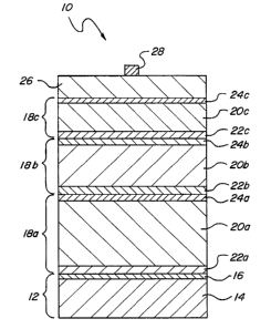
Brief Description of the Drawing
FIGURE 1 is a cross-sectional view of a tandem
photovoltaic device structured in accord with the
principles of the present invention.
Detailed Description of the Invention
Referring now to Figure 1, there is shown a
tandem photovoltaic device 10 of the type which may be used
in conjunction with the present invention. The device 10
comprises a stacked array of photovoltaic cells 18a - 18c
interposed between a substrate electrode 12 and a top
electrode 26.
The device 10 is fabricated upon a substrate 12
which supports the overlying semiconductor layers and .
provides a bottom electrode for the device. The substrate
12 may comprise a body of stainless steel or other such
metal or it may comprise an electrically insulating
material, such as a polymer, ceramic or glass, with an
electrically conductive coating thereupon. In the
~WO 94/14199 ~ PCT/US93/11697
-
illustrated embodiment, the substrate 12 is a composite
substrate formed of an electrically conductive, base 14,
preferably of stainless steel; having a light reflective
coating 16, such as a layer of silver or aluminum
thereupon. In this instance, the reflective coating 16
serves to further enhance the efficiency of the
photovoltaic device by redirecting any unabsorbed
illumination back therethrough. In some instances a layer
of an electrically conductive, substantially transparent
material such as zinc oxide may be disposed atop the
reflective layer 16. As is well known in the art, there
exist various configurations of back reflectors for use in
photovoltaic devices, all of which may be employed in
connection with the present invention. Therefore in the
context of this disclosure, the term "substrate" shall
include metallic substrates as well as electrically
insulating substrates having conductive coatings thereupon,
and shall further include any light reflective structures
associated with the substrate.
Disposed atop of the substrate 12 is a first
photovoltaic cell 18a. This cell is of P-I-N type
configuration and includes a body of substantially
intrinsic semiconductor material 20a interposed between a
layer of P-doped semiconductor material and a layer of N-
doped semiconductor material. In the illustrated
embodiment, the layer of N-doped material 22a is closest to
the substrate and the layer of P-doped material 24a is
disposed on the opposite side of the intrinsic body 20a.
It is to be understood that the location of the P-doped
WO 94/14199 PCT/US93/11697
~ ~. ~ 1'~ 3 G
_8_
layer 22a and N-doped layer 24a may be exchanged in some
instances. It should also be kept in mind that the layer
of intrinsic material 20a is referred to as a layer of ,
'°substantially°' intrinsic material in view of the fact that
n
such material may have a slight P-doping therein or a
slight N-doping therein. As is well known to those of
skill in the art, in a P-I-N type photovoltaic device, the
absorption of illumination in the intrinsic layer creates
electron-hole pairs which are separated by a field
resultant from the presence of the doped layers. The
separated carriers are collected and contribute to the
photocurrent generated by the cell.
A tandem photovoltaic device includes at least
two stacked photovoltaic cells; and within the context of
this disclosure, the device 10 includes a second
photovoltaic cell 18c in superposed relationship with the
first cell 18a. The second cell 18c includes a
substantially intrinsic body of semiconductor 20c
interposed between a layer of N-doped semiconductor
material 22c and a layer of P-doped semiconductor material
24c. The tandem device may include further cells
interposed between the first cell 18a and second cell 18c:
and as illustrated herein, the device 10 includes a third
cell 18b which is comprised of a layer of substantially
intrinsic semiconductor material 20b interposed between N-
doped 22b and P-doped 24b semiconductor layers. ,
The device 10 further includes a top electrode
26, which in this particular embodiment is a light
transmissive electrode fabricated from a transparent
WO 94/14199 ~' PCT/US93/11697
_ g _
conductive oxide (TCO) material such as indium oxide, tin
oxide, zinc oxide and various other such materials, taken
either singly or in combination. As is further illustrated
in the figure, the device also includes an electrically
conductive grid 28'disposed atop the top electrode 26. The
grid 28 is fabricated from a high conductivity material
such as a metallic paste or foil and operates to collect
photo generated current from the top electrode 26 and to
carry it to a collection point. In some instances, the
tandem photovoltaic device may be fabricated in an inverted
configuration wherein the substrate 12 is electrically
conductive and transparent and the top electrode 26 is
metallic.
In the photovoltaic device 10 of higure 1, light
passes through the transparent top electrode 26 and is
first absorbed by the second cell 18c so as to generate a
photocurrent. The unabsorbed light passes through the
second cell 18c to the third cell 18b where a portion is
absorbed to generate another photocurrent. The remaining
light passes through to the first cell 18a where it is
absorbed to generate a photocurrent. Any remaining
unabsorbed light is redirected by the reflective layer 16
for a second pass back through the stacked cells.
Since light passes in sequence through the
devices they are said to be disposed in an optical series
arrangement. The cells are also in an electrical series
relationship. It will also be noted that the intrinsic
layers 20 of the cells 18 vary in thickness. The reason
for the thickness variation is to equalize the photocurrent
WO 94/14199 PCTlUS93/11697
-
~~ -
produced by each of the cells 18a, since conventional
wisdom has heretofore held that maximum device efficiency
is obtained when currents are matched. As light passes ,
through the device 10 it is attenuated, and hence the
bottom most intrinsic layer 20a must be thicker than the
top most intrinsic layer 20c if equal currents are to be
produced in the first 18a and second 18c cells.
As noted above, the various cells 18 of the
device 10 may have intrinsic layers 20 which are all of the
same band gap or they may have intrinsic layers 20 which
differ in band gap. The absorption of light by a
semiconductor material is determined by its band gap, and
wide gap materials have an optical absorption beginning at
higher energies (optical edge) than do materials having a
lower band gap. Therefore, in the fabrication of a multi
gap tandem device, the bottom most intrinsic layer is made
from a relatively narrow band gap material and the top most
layer is made from a relatively wide band gap material. In
this manner, the top-most cell will absorb only the shorter
wavelength illumination and the bottom most cell will
primarily function to absorb longer wavelength
illumination.
In one typical tandem photovoltaic device the
substrate 12 comprises a layer of stainless steel and the
first cell 18a includes an amorphous silicon-hydrogen-
germanium alloy intrinsic layer of approximately 2000
angstroms thickness interposed between relatively thin
layers of N-doped 22a and P-doped 24a silicon-hydrogen
alloy material. In a most preferred embodiment, the layer
~WO 94/14199 PCT/LTS93/11697
- 11 -
of P-doped material 24a is a micro crystalline layer. In
this embodiment the intermediate cell 18b includes an
approximately 3000 angstrom thick intrinsic amorphous
silicon-hydrogen alloy layer 20b interposed between N-doped
22b and P-doped 24b layers as previously noted. In this
embodiment the topmost cell 18c is generally similar to the
intermediate cell 18b except that the intrinsic layer
thereof 20c is approximately 800 to 1000 angstroms in
thickness.
As noted above, conventional wisdom has dictated
that cell thicknesses should be optimized so as to match
the currents produced thereby in order to provide optimum
device performance. It has been found, in accord with the
principles of the present invention, that in a tandem
device, the cell producing the lowest current tends to
dominate the properties of the overall device. That is to
say, the contribution of a low current cell to the overall
performance of the device is disproportionate compared to
the contribution of the remaining cells. ~s noted above,
cell performance will depend, to a large degree, upon the
quality of the material comprising the intrinsic layer of
the cell. One measure of cell performance is the fill
factor of the cell. Fill factor is a device parameter
recognized in the art and is determined from the
characteristic current-voltage curve of the device when it
is subjected to illumination. In generating a curve of
this type, photogenerated voltage is measured as a function
of the load applied to the cell as the load varies from a
short circuit condition to an infinite load (i.e., open
WO 94/14199 PCT/US93/11697
- 12 -
circuit), and a series of points are graphed from this data
so as to define the characteristic curve of the device.
Fill factor is a measure of deviation of the area under
this curve from an ideal condition and the closer in value
i
the fill factor is to 1.0 the more useful power is provided
by the cell.
It has been found that the dual tandem device
wherein the fill factor of the top cell and the fill factor
of the bottom cell are of equal value, for example, a value
of 10~ below theoretical, the overall fill factor of the
resultant tandem device will be of the same value, namely
10~ less than ideal. However, if the fill factor of the
upper cell is 10~ less than ideal and that of the lower
cell is 20~ less than ideal, the overall device fill factor
will be approximately 12% less than ideal if the first cell
is the dominant cell and it will be approximately 18~ less
than ideal if the second cell is the dominant cell.
Similar values hold for the converse situation wherein the
upper cell is of lower quality.
The present invention represents a departure from
prior art teachings regarding tandem photovoltaic devices.
The prior art has taught that photocurrents from the cells
of a tandem device need to be matched. The present
invention recognizes that the cell producing the lowest
current contributes disproportionately to the device
performance; and in accord with the present invention, it
is taught that overall device performance can be
significantly improved, and an optimum balance between
manufacturing and operational efficiency can be achieved,
~O 94/14199 ~ PCT/US93/11697
- 13 -
by fabricating the highest quality cell of a tandem voltaic
device so that it is the dominant cell. Therefore, the
device is fabricated so that the cell having the best
material properties produces a somewhat lower photocurrent
under illumination than do the remaining cells.
Generally, it has been found that lower deposition rate
processes result in the preparation of higher quality
materials, albeit at the expense of some manufacturing
efficiency. For this reason it is generally preferable
that the topmost cell of the tandem device, which is the
thinnest cell, is fabricated from a slowly deposited, high
quality material and that it be configured to be the
dominant cell.
Vacuum deposition processes, as is well known in
the art, include evaporation and sputtering processes as
well as glow discharge deposition processes. Glow
discharge deposition processes are generally preferred for
the preparation of thin film semiconductor materials,
particularly Group IVA semiconductor materials. In
processes of this type, as is well known in the art, an
input of electromagnetic energy is employed to generate a
plasma from a process gas mixture which is maintained at
subatmospheric pressure. In the plasma the process gas is
decomposed to create deposition species which impinge upon
a substrate so as to deposit a semiconductor layer. Such
techniques are disclosed, for example in U.S. Patent
4,226,898 and U.S. Patent 4,517,223. As detailed therein,
electromagnetic energy may comprise do energy, radio
frequency energy or microwave energy, and it has been found
WO 94/14199 ' PCTIUS93/11G97
- 14 -
that microwave energized deposition processes tend to be
highly efficient in terms of gas utilization and deposition
rates, and radio frequency energized processes, while
somewhat slower, produce higher quality semiconductor
deposits.
In accord with one embodiment of the invention,
a tandem photovoltaic device is fabricated by a process
wherein the bottom most, relatively thick cell is
fabricated in a high rate, microwave energized deposition
process and the top most, relatively thin cell is a higher
quality device which is preferably deposited in a radio
frequency energized process. The top cell is made somewhat
thinner than dictated by conventional wisdom so that it
will produce a photocurrent less than the photocurrent
produced by the bottom most cell. Since the dominant top
cell is relatively thin, the increase in deposition rate
and/or machine size attributable to the use of a slow
deposition rate process will have a minor adverse effect
upon the manufacturing efficiency of the device and will be
offset by the increase in operational efficiency thus
obtained.
experimental
A series of P-I-N type photovoltaic devices and
two tandem devices were prepared in accord with the
principles of the present invention. The devices were
prepared upon stainless steel substrates by a radio
frequency energized glow discharge deposition process.
WO 94/14199 _ ~ ~ ~ I '~ 3 ~ PCT/US93/11697
- 15 -
In order to prepare a first P-I-N device, a
substrate was placed in a deposition chamber which was
sealed from the ambient atmosphere, and an atmosphere
comprising 20 SCCM of hydrogen, .75 SCCM of a 1~ mixture of
phosphine in hydrogen and .65 SCCM of disilane was flowed
therethrough. A pump associated with the deposition
apparatus was adjusted to maintain a pressure of 1.2 torr
therein. The substrate was heated to a temperature of 350
C. and the gas mixture energized with radio frequency
energy of 13.56 mhz from a cathode of approximately 3.5
inches in diameter at a power of 2 watts. Deposition
conditions were maintained until approximately 200
angstroms of N-doped silicon alloy material was deposited
on the substrate at which time cathode power was
terminated. An 800 angstrom thick intrinsic layer was then
deposited atop the N-doped layer and toward that end, a
deposition atmosphere of 20 SCCM of hydrogen and .65 SCCM
disilane was flowed through the chamber at a pressure of
1.2 torr. The substrate was maintained at ?.25~ C. and the
cathode energized as before for a time sufficient to
deposit an 800 angstrom thick layer of intrinsic material
at a deposition rate of 2.2 angstroms per second. In the
final stage, a microcrystalline, P-doped layer was
deposited atop the intrinsic layer by use of an atmosphere
of 95 SCCM of hydrogen, 3.25 SCCM of a 2~ mixture of BF3 in
hydrogen and 2.5 SCCM of a 5~ mixture of silane in
hydrogen, which was flowed through the chamber at a
pressure of 1.77 torr. The cathode was energized as before
and deposition conditions maintained for 65 seconds. The
WO 94/14199 PCT/US93/11697
~~~~~3~
- 16 -
thus fabricated device was provided with a transparent
conductive oxide top electrode in a conventional vacuum of
evaporation process.
Operational parameters of thus completed
photovoltaic cell were measured under the illumination of
a AM 1.5 solar spectrum. Measurements were made on the
device as prepared and after 600 hours of exposure to the
AM 1.5 solar spectrum. The initial efficiency of the cell
was 4.97% and after photo degradation it was 4.33% The
fill factor of the cell as prepared was .76 and after
degradation it was .703.
A second P-I-N cell was prepared as in the
previous example except that the deposition rate of the
intrinsic layer was 20 angstroms per second and the
thickness of the intrinsic layer was 1000 angstroms. This
cell manifested an initial efficiency of 4.52% and an
efficiency, after 600 hours of exposure of 3.27%. The fill
factor of the freshly prepared cell was .70 and the fill
factor of the cell after degradation was .575.
Two tandem photovoltaic devices were deposited on
stainless steel substrates precoated with a back reflector
structure comprising a layer of silver covered with a layer
of electrically conductive zinc oxide. The deposition
techniques were in accord with the prior experiments. Both .
devices included substantially identical bottom cells
fabricated from a layer of substantially intrinsic
amorphous silicon: germanium: hydrogen, interposed between
p and n doped layers as noted previously. The intrinsic
layers of the top cells of the tandem devices comprised
2~.~~.?36
~WO 94114199 ' PCT/US93/11697
- 17 -
amorphous silicon: hydrogen and were both deposited at a
temperature of 300 C. The intrinsic layer of the first
device (L5319) was deposited at 1.2 A/Sec and that of a
second (L5320) at 8.8 A/Sec. The operational parameters of
both devices were measured after preparation and after 163
hours of light soaking under a simulated AM 1.5 solar
spectrum. The parameters are reported in table 1 below,
and it is clear that the device in which the top cell is
deposited at the high rate, degrades more.
TABLE I
Js~ Voc FF
(mA/cm ) (Volts)
L5319 10.04 1.59 0.69 10.94 -
INITIAL
LIGHT-SOAKED 9.92 1.55 0.65 9.96 9.0
FOR 163 HOURS
L5320 9.58 1.60 0.66 10.11 _
INITIAL
LIGHT-SOAKED 9.24 1.53 0.57 8.04 20.5
FOR 163 HOURS
It will thus be seen from the foregoing that
tandem photovoltaic devices having improved efficiencies
may be fabricated by controlling the geometry and material
properties of the layers of the device. Specifically the
thickness of the respective intrinsic layers of the cells
of the tandem device is controlled so that the cell having
the best material quality is the cell producing the lowest
photocurrent. This approach, while counter-intuitive,
assures that the material properties of the cell fabricated
from the best material will dominate the operational
parameters of the tandem device. Ideally, the thinnest
WO 94/14199 ~ ~~ .~~ ~ PCT/US93/11697
- 18 -
cell of the device will be fabricated by a low deposition
rate process so as to provide superior material properties,
and the thickness of the intrinsic layer of that particular
cell will be made slightly lessernthan needed to match the
currents of the remaining cells of the device.
It will be appreciated that a variety of specific
processes may be implemented in accord with this broad
principles, to enable the fabrication of a variety of
differently configured tandem photovoltaic devices. For
example, deposition may be accomplished by microwave
processes, radio frequency energized processes, do
energized processes as well as thermally energized chemical
vapor deposition processes and combinations thereof, to
achieve the appropriate thickness and material quality
parameters. The principles of the present invention may be
adapted to all tandem devices having two or more cells
whether they are same gap or multiple gap devices. Thus,
it will be appreciated that the foregoing drawing,
discussion, description and examples are merely meant to
illustrate particular embodiments of the present invention
and are not meant to be limitations upon the practice
thereof. It is the following claims, including all
equivalents which define the scope of the invention.