Note: Descriptions are shown in the official language in which they were submitted.
2_1Sll ~5
Resonance Converter
RACR~-ROUND OF THE lNV~N-llON
1. Field of the Invention:
The present invention relates to a resonance
converter, and in particular to a high-output resonance
converter of the current resonance type.
2. Description of the Related Art:
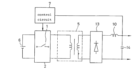
Prior art resonance converters of this type are
constructed as shown in Fig. l. In this figure, the
power outputted by direct current power source 6 is
on/off controlled by switching circuit 2 and supplied
to the primary side of insulating transformer 5, the
induced power from the secondary side of this
transformer 5 is converted to direct current power by
rectifying circuit 13 and smoothing circuit (composed
of choke coil 10 and condenser 14) and supplied to a
load not shown.
This direct current output voltage is inputted to
controller 7 for carrying out on/off control of
switching element l (usually, an FET element or a
bipolar transistor element) of switching circuit 2
according to the voltage level of the direct current
output voltage for the purpose of stabilizing the
direct current output.
A series resonance circuit having resonance coil 3
2151 79.~
and resonance condenser 4 is provided on the primary
side of insulating transformer 5, and a resonance
converter is formed by arranging insulating transformer
5, which is the load, in parallel with resonance
condenser 4. Resonance is generated between resonance
coil 3 and resonance condenser 4 by turning on
switching element 1, and a resonance current is
supplied to insulating transformer 5, which is the load.
If switching element 1 is turned off when this
resonance current is zero, switching loss at the
switching element, which can be expressed as (current)
x (voltage), theoretically becomes zero, and a highly
efficient high-power output can be obtained from the
circuit on the secondary side.
When using this type of prior art resonance
converter in switching large currents, however, the
resonance condenser is prone to deterioration due to
ripple current or saturation in the resonance coil,
while the use of a large resonance coil and resonance
condenser necessitates more installation space and
makes it difficult to provide a smaller, lighter, and
less expensive converter.
SUMMARY OF THE lNv~NllON
The object of the present invention is to provide
a resonance converter in which the entire circuit can
215~ 795
be made compact, light, and inexpensive by reducing the
size of the resonance coil and resonance condenser.
According to the present invention, a resonance
converter may be obtained which comprises an insulating
transformer, switching means for on/off control of the
electrical power impressed to the primary side of the
insulating transformer, and smoothing-rectifying means
for smoothing-rectifying the induced power on the
secondary side of the insulating transformer, and which
is characterized by having a resonance circuit
constituted by the leakage inductance and distributed
capacity of the insulating transformer.
In particular, in an insulating transformer having
high-voltage output greater than 1 KV, this leakage
inductance on the secondary side is several tens of
times greater than the leakage inductance on the
primary side. As a result, the resonance frequency
characteristic of the insulating transformer is
dominated by the resonance frequency due to secondary
side leakage inductance and distributed capacity.
In the present invention, this leakage inductance
and distributed capacity of the high-voltage output
insulating transformer is used constructively in the
resonance circuit to enable a compact and light-weight
device.
The above and other objects, features, and
21 ~1 7~
-- 4
advantages of the present invention will become
apparent from the following description based on the
accompanying drawings which illustrate an example of a
preferred embodiment of the present invention.
BRIEF DESCRIPTION OF THE DRAWINGS
Fig. 1 is a block circuit diagram of a resonance
converter of the prior art;
Fig. 2 is a block circuit diagram of one
embodiment of the present invention;
Fig. 3 shows operation wave forms of the circuit
shown in Fig. 2;
Fig. 4A is a block circuit diagram of another
embodiment of the present invention, and Fig. 4B is a
block circuit diagram of yet another embodiment of the
present invention; and
Fig. 5 is an equivalent circuit diagram of an
insulating transformer used in the embodiments of the
present invention.
DETATT~n DESCRIPTION OF THE PREFERRED ~MRODTM~NTS
Embodiments of the present invention will next be
explained with reference to the figures.
Fig. 2 is a circuit diagram of one embodiment of
the present invention in which the same reference
numerals are used for parts equivalent to those shown
21 Sl 79~
in Fig. 1. In this embodiment, an insulating transformer
of high-voltage output (1 KV or greater) is used as
transformer 5. The leakage inductance and distributed
capacity on the secondary side of this transformer are
constructively used as a resonance element, thereby
dispensing with the resonance coil 3 and resonance
condenser 4 used in the prior art converter of Fig. 1.
An equivalent circuit of this insulating
transformer 5 is shown in Fig. 5. Here, the portion
indicated by reference numeral 20 is an ideal
transformer, on the primary side of which exist
distributed capacity 9, leakage inductance 8,
equivalent resistance 21, and in addition, a parallel
circuit having resistance 22 and inductance 23 of the
primary side coil. In addition, the secondary side has
distributed capacity 9', leakage inductance 8', and
equivalent resistance 21', and distributed capacity 24
exists between the primary and secondary sides.
In this case, if a device in which an insulating
transformer of high-voltage output of at least 1 KV is
used, as described hereinabove, secondary side leakage
inductance 8' is several tens of times greater than the
primary side leakage inductance 8, and the resonance
frequency characteristic of this transformer 5 will be
dominated by a frequency due to this secondary side
leakage inductance 8' and distributed capacity 9'.
21~1 79~
The smoothing circuit which smoothes the rectified
output of rectifying circuit 13 is constructed as a
choke input type, and the secondary side load of
transformer 5 is of high impedance, and a resonance
current can therefore be efficiently generated on the
secondary side of transformer 5.
Since this resonance on the secondary side is the
load as seen from the primary side of transformer 5,
the primary side current also forms a resonance wave
form, and as shown in Fig. 2, when the primary side
resonance current wave form reaches a minimum value or
zero, frequency control is performed at control circuit
7 such that switching element 1 is turned off, thereby
allowing efficient transmission control of electrical
energy from the primary side to the secondary side of
transformer S.
Figs. 4A and 4B each show another embodiment of
the present invention, identical reference numerals
being used for parts equivalent to those shown in Fig.
2. Fig. 4A shows an example in which a condenser 12 for
resonance frequency regulation is parallel connected in
the secondary output portion of transformer 5.
By selecting the capacitance of this condenser 12,
variation in the resonance frequency that is caused by
variance in the distributed capacity and leakage
inductance of transformer 5 can be absorbed and made
2~1795
uniform, thereby enabling a constantly correct
frequency. Fig. 4B shows an example in which a
condenser 12 for resonance frequency regulation is
parallel connected in the output portion of rectifying
circuit 13.
The condenser 12 for resonance frequency
regulation in both Figs. 4A and 4B is for regulation
and its capacitance should therefore be small, with the
result that the addition of this condenser 12 will not
cause a decrease in the load impedance on the secondary
side of transformer 5.
As described hereinabove, according to the present
invention, a resonance current is generated by
constructively using the leakage inductance and
distributed capacity of an insulating transformer to
make up a resonance circuit, thereby eliminating the
need for a resonance coil and resonance condenser and
enabling a device that is not only more compact and
light-weight, but also less expensive.
In addition, when adjusting resonance frequency, a
favorable effect can be obtained by merely adding a
condenser of small capacitance.
It is to be understood, however, that although the
characteristics and advantages of the present invention
have been set forth in the foregoing description, the
disclosure is illustrative only, and changes may be
21 51 795
made in the arrangement of the parts within the scope
of the appended claims.