Note: Descriptions are shown in the official language in which they were submitted.
WO 94/15169 PCTIUS93/12319
21~1911
DIGITAL DELAY UNIT
BACRGROUND OF T~E: 1NV~:Nl ION
5 Field of the Invention
This invention relates to detonation devices using
electronic delay timing for use with non-electric blasting
initiation systems.
Backqround and Related Art
Blasting operations normally involve sequentially
timed detonations of explosive charges placed within bore-
holes drilled into the earth, for example, into a rock or
ore mass to be fragmented. Generally, one or more trans-
mission lines are deployed from a central initiating pointto send a signal to detonate the individual blasting
charges located within the respective boreholes. These
transmission lines may consist of one or more trunklines
connected to a plurality of "downlines" leading from the
trunklines into the boreholes to transmit the initiating
signal to a detonator, sometimes referred to as a blasting
cap, which, upon detonation, generates a shock wave that
detonates the main explosive charge within the borehole.
The timing of sequential detonations within each borehole
must be closely controlled to achieve the desired fragmen-
tation and movement of ore and rock. The time intervals
between borehole detonations are on the order of millisec-
onds to achieve the desired results and are attained by
providing a delay between the time the initiating signal
is received by the detonator and the detonation of the de-
tonator. Generally, at least an eight millisecond delay
is required between adjacent boreholes, and significantly
longer millisecond delays are o~ten used.
In non-electric blasting systems the requisite delay
periods may be obtained by the use of blasting caps and/or
in-line signal transmission caps which contain a pyrotech-
nic delay composition. As is well-known in the art, these
delay compositions provide a length of material within the
WO'94/15169 21~191 1 PCT~S9311~19
.~_
--2--
detonation train of the caps which burn at a controlled
rate to provide a preselected delay, e.g., 25, 50, 250 or
500 milliseconds, between the receipt of an incoming deto-
nation signal and the detonation of the primary charge
within the cap to transfer the detonation signal to the
main explosive charge in a borehole or to another length
of signal transmission line. The provision of such pyro-
technic delays in blasting caps is illustrated in U.S.
Patent 3,987,732 to Spraggs et al, which describes a de-
vice utilizing a pair of blasting caps having differentdelay periods. However, such pyrotechnic delays exhibit
inherent variances in burn time and hence, in the desired
delay interval. Consequently, the exact delay periods as-
sociated with a given blasting cap varies within a range
which depends on the manufacturing tolerances. This burn
time variance, which results from compositional and manu-
facturing variances which, as a practical matter, are una-
voidable, leads to time scatter or inaccuracy associated
with the delayed ignition of the borehole charges. The
variation or scatter of the ignition times can result in
poor rock fragmentation and possibly damage outside the
blast zone. If the time between sequential detonations is
very short, for example, at or near the eight millisecond
minimum, the time scatter resultinq from burn time vari~-
tions may approach or even exceed the programmed interval,thus resulting in out-of-sequence detonation of adjacent
boreholes.
Conventional detonatinq cords are noisy and have a
tendency to throw debris and shrapnel from destroyed con-
nectors and the like, which may result in cutting thetransmission line ahead of the signal, thereby disrupting
the desired blasting pattern. These disadvantages in a
transmission line may be overcome by the utilization of
known, non-destructive signal transmission lines. One
type is commonly referred to as "shock tube" and is illu-
strated in Thureson et al U.S. Patent 4,607,573. Other
non-destructive transmission lines include low velocity
signal transmission tubes as illustrated in Thureson et al
WO94/15169 21 51 91 1 PCT~S93/1~19
~_,
--3--
U.S. Patent 4,757,764. Shock tube and low velocity signal
transmission tube ("LVST tube") generally comprise hollow,
plastic tubing which is coated on its interior surface
with a thin layer of a suitable explosive (shock tube) or
deflagrating composition (LVST tube). Upon initiation of
the explosive or deflagrating composition within such sig-
nal transmission tubes, a shock wave, flame front or other
such impulse signal is transmitted through the tube. This
impulse signal may be utilized to detonate signal trans-
mission and blasting caps in order to initiate timed de-
tonation of the main charges.
As indicated above, the use of pyrotechnic delay de-
vices in signal transmission lines is known in the art.
For example, a pyrotechnic delay unit for a signal trans-
mission tube is shown in U.S. Patent 4,742,773, issued toBartholomew et al, on May 10, 1988. This Patent calls for
using, in a signal transmission tube, a delay assembly
comprising a delay element which contains a shaped pyro-
technic delay composition having a pre-selected combustion
time. As described beginning at column 3, line 49 of the
Bartholomew Patent, signal transmission tubes are received
in the opposite ends of the delay assembly and connected
to opposite ends of the delay element. An incoming im-
pulse signal from one of the transmission tubes connected
to the assembly initiates the timed combustion of the de-
lay element, starting at one end thereof. The combustion
time of the delay element may range from nine milliseconds
to ten seconds or longer, depending on the delay composi-
tion utilized (column 4, lines 11-15). When the combus-
tion proceeds from one end to the other end of the delayelement, the pre-selected delay period will have elapsed
and the burning delay element ignites the other, outgoing
signal transmission tube. Consequently, a selected delay
in timing of transmission of the signal through the trans-
mission tube connected by the delay unit is attained. Thepyrotechnic delay assembly of the Bartholomew Patent em-
ploys transition and delay chemical compositions compris-
ing various reactive chemical compounds, as explained be-
W0~4/15169 2 1 5 1 9 1 1 PCT~S9311~19
--4--
ginning at column 4, line 38.
The use of electrically-initiated detonators which
contain pyrotechnic delays is, of course, subject to the
same problems as described above with respect to non-elec-
trically-initiated systems insofar as inherent variances
of burn time of the detonator delays is concerned. The
use of electrical blast sequencing machines in conjunction
with instant detonators or electronically-timed detona-
tors, while capable of providing accurate borehole-to-
borehole time delays, requires an electrical potential ofhundreds of volts to reliably ignite all of the large num-
ber of blasting caps used in such systems, and such volt-
ages pose sometimes lethal safety hazards to workers in
the field. On the other hand, only a relatively small
amount of energy is required for the ignition of an indi-
vidual electric blasting cap so that premature or unin-
tended detonations can be caused by static electricity,
ground currents, currents induced by power lines, radio-
frequency or microwave sources or other sources of rela-
tively low energy electromagnetic noise. Further, theinterconnection of electric blasting caps in large blast
patterns can be extremely complex and an error in calcula-
tions could result in failure of the detonation of one or
more detonator caps, resulting in the very hazardous situ-
ation of undetonated main explosive charges in the muckpile caused by those charges which did explode.
U.S. Patent 5,173,569, dated December 22, 1992 des-
cribes an electrical delay detonator (blasting cap) for
use in non-electric blasting systems which enables the at-
tainment of a pre-selected delay in detonation of the de-
tonator's output charge in response to the arrival of an
incoming non-electric signal through the use of an elec-
tronically timed delay circuit disposed within the deto-
nator. This Patent details the use of a transducer, e.g.,
a piezoelectric element which is responsive to a pressure
wave generated by detonation o~ a booster charge which is
detonated by an incoming non-electric impulse signal,
e.g., from a shock tube, to power an electronic circuit
--5--
providing a preset, solid state-controlled time delay for detonation of the detonator
and thereby of the explosive charges served by the detonator. The disclosure of
U.S. 5,173,569 discloses a device in which the power generated by pressurizing
the transducer is the source of a power needed to initiate and operate the delay5 circuitry as well as to activate, i.e., detonate, the booster charge. The limited
amount of energy available by pressurization of the tr~n~dllcer necessarily limits
the duration ofthe delay which can be attained. The device of U.S. 5,173,569
required a booster charge to activate the transducer; the booster charge may be
omitted if the input tr~n~mi~ion line has sufficient energy to reliably energize the
0 transducer, e.g., if the input tr~n~mi~ion line is a low energy detonating cord.
SUMMARY OF THE INVENTION
Generally, the present invention provides a delay unit cont~inin~; an output
charge, e.g., a delay detonator, adaptable for in-line or downhole use which, in one
embodiment, utilizes cil.;uiLly which includes an energy source such as battery
means which is used to supply power to the delay circuit upon activation by a
signal received from the energized transducer. The battery means or the like is
designed to provide sufficient energy to power the delay circuit even for an
extended duration of delay, but the energy available from the battery means is
2 o limited so that even in the event of a short circuit or other malfunction, the energy
output of the battery means is insufficient to detonate the output charge. In
another embodiment of the invention, the delay unit includes one or more output
line retainer means for retaining one or more output tr:~n~mi~ion lines in
proximity to the output charge whereby detonation of the output charge ignites the
25 one or more output tr~n~mission lines.
Specifically, in accordance with the present invention, there is provided an
electrical delay unit, e.g., a delay detonator, for use in blasting initiation systems
V
WO94115169 PCT~S93/1~19
2151911
'".,
--6--
energized by a non-electric impulse signal. The delay
unit comprises a housing means, e.g., a tubular, electric-
ally conductive body, having one end thereof dimensioned
and configured to be coupled to an input transmission
line. The input transmission line may be, e.g., an input
transmission tube such as a shock tube, or it may be a low
energy detonating cord. In any case, the input transmis-
sion line is capable of transmitting an input non-electric
impulse signal. The housing means, which may be closed at
the end opposite the aforesaid one end, has: (i) a signal
conversion means disposed in signal-communicating rela-
tionship to the transmission line for receiving an impulse
signal from the transmission line and converting the im-
pulse signal to an electrical output signal, and (ii) an
electric circuit including delay means having an output
conductor means. The electric circuit is connected to the
signal conversion means to receive from it the electrical
output signal and thereupon start counting a selected time
interval. Upon lapse of the time interval, the electrical
output signal is trA~s~itted by the electric circuit to
the output conductor means. The delay unit of the present
invention further comprises (iii) an electrically operable
igniter means contained in the housing means and connected
to the output conductor means of the electric circuit and
to an output charge. The igniter means is energized to
detonate the output charge upon receipt of the electrical
output signal from the electric circuit.
In accordance with one aspect of the present inven-
tion, the electric circuit includes a battery means con-
nected thereto to supply the electric circuit with powerfor counting the selected time interval upon receipt by
the electric circuit of the electrical output signal.
Another aspect of the present invention provides that
the power output of the battery means is insufficient to
energize the igniter element sufficiently to detonate the
output charge.
In another aspect of the invention, the electric cir-
cuit comprises an oscillator for generating cycles con-
WO'~4115169 PCT~S93/1~19
2151911
_ -7-
nected to the battery means to receive power therefrom for
generating the cycles, a counter connected to the oscilla-
tor for counting the cycles, and means for preloading the
counter with an initial value. There may be a voltage re-
gulator connected to the energy storage means.
According to still another aspect of the invention,
the housing means may comprise one or more output line
retainer means for retaining one or more output transmis-
sion lines in proximity to the output charge whereby deto-
nation of the output charge can ignite one or more outputtransmission lines disposed therein.
Yet another aspect of the present invention provides
for the inclusion of a booster charge disposed within the
housing and positioned to be detonated by the impulse sig-
nal received from the input transmission line to amplifythe impulse signal received by the signal conversion.
Other aspects of the invention provide for the elec-
tric circuit to comprise means to convert the electrical
output signal to a first signal which starts the counting
of the time interval and a second signal which energizes
the igniter element at the end of the time interval; other
aspects of the invention provide for the signal conversion
means to comprise (a) a transducer, e.g., a piezoelectric
qenerator, for converting the input impulse signal to
electrical energy and (b) an energy storage means, e.g., a
storage capacitor, connected to the transducer to receive
therefrom and store electrical energy for release from the
energy storage means as the electrical output signal.
Any of the foregoing embodiments may include an input
transmission line, e.g., an input transmission tube, e.g.,
a shock tube, or a low energy detonating cord coupled
thereto. Some embodiments may include programming means
carried by the housing. The programming means is effec-
tive to program the duration of the time interval of the
delay circuit. Optionally, the programming means may be
accessible from the exterior of the housing and may fur-
ther include an interface connector connecting the pro-
gramming means to the delay circuit whereby the duration
~ -8- ~ 7 t
of the time interval of the delay circuit may be
programmed. The interface connector may comprise an
inductive, pick-up means.
A method aspect of the present invention provides
for interposing a time delay between the application of
an input non-electric impulse signal received from a
transmission line and the detonation of an output charge.
The method comprises the following steps. (a) Converting
the input impulse signal to a first electric signal.
This step may be carried out by pressurizing a piezo-
electric generator with the impulse input signal. The
input signal may optionally be amplified by using it to
detonate a booster charge which in turn pressurizes the
piezoelectric generator. (b) Transmitting the first
electric signal to an oscillator. (c) Counting the number
of cycles generated by the oscillator in response to the
first electric signal; the power to carry out this step
may optionally be supplied from a battery means. (d)
Generating a second electric signal upon the completion
of a preprogrammed count of the number of cycles. (e)
Transmitting the second electric signal to an
electrically operable output charge to detonate the
output charge. Optionally, the method may comprise using
the energy of the output charge to ignite one or more
output transmission lines, to emit one or more output
signals.
Other aspects of this invention are as follows:
An electrical delay unit for use in blasting
initiation systems energized by a non-electric impulse
signal comprises a housing means having one end thereof
dimensioned and configured to be coupled to an input
transmission line capable of transmitting a non-electric
impulse input signal has: (i) a signal conversion means
.~
~ ~ 5 ~ z~
_ -8a- -
disposed in signal-communicating relationship to the
transmission line for receiving a non-electric input
impulse signal from the transmission line and converting
the impulse signal to an electrical output signal: (ii)
an electric circuit including delay means having an
output conductor means, the electric circuit being
connected to the signal conversion means to receive
therefrom the electrical output signal and thereupon to
start counting a selected time interval and, upon lapse
of the time interval, to transmit the electrical output
signal to the output conductor means; the electric
circuit further including a battery means connected
thereto to supply power for counting the selected time
interval independently of the electrical output signal;
(iii) an electrically operable igniter means connected to
the output conductor means of the electric circuit and to
an output charge; the igniter means being energized to
detonate the output charge upon receipt of the electrical
output signal from the electric circuit.
A method for interposing a time delay between the
application of a non-electric impulse input signal
received from an input transmi~sion line and the
detonation of an output charge, comprising the steps of:
(a) converting the non-electric input impulse
signal to a first electric signal;
(b) transmitting the first electric signal to
an oscillator;
(c) counting the number of cycles generated by
the oscillator in response to the first electric signal
by employing an electronic timer;
(d) generating a second electric signal upon
the completion of a preprogrammed count of the number of
cycles,
(e) transmitting the second electric signal to
an electrically operable output charge to detonate the
output charge; and
-8b-
(f) supplying power to carry out the counting
of step (c) independently of the first electric signal.
These and other aspects of the present invention,
together with objects and advantages thereof, will be
apparent in the details of construction and operation as
more fully hereinafter described and claimed, reference
being had to the accompanying drawings forming a part
hereof.
BRIEF DESCRIPTION OF THE DRAWINGS
Figure l is a schematic view partly in cross section
showing one embodiment of a delay detonator of the
present invention having a shock tube input transmission
line coupled thereto;
Figure lA is a view, on a scale which is enlarged
relative to Figure 1, of the isolation cup and booster
W0~4/15169 PCT~S93/1~19
2151911
charge components of the detonator of Figure l;
Figure lB is a partial schematic view partly in cross
section showing a second embodiment of a delay detonator
of the present invention having a low energy detonating
cord input transmission line coupled thereto;
Figure 2 is a schematic cross-sectional view showing
one embodiment of a delay unit of the present invention
including an input transmission line and an output trans-
mission tube attached thereto;
Figure 2A is a view, enlarged relative to Figure 2,
of the low energy booster detonator of the delay unit of
Figure 2 and certain connections thereto;
Figure 2B is a view, enlarged relative to Figure 2,
of the output detonator of the delay unit of Figure 2 and
certain connections thereto;
Figure 2C is a schematic block diagram representing
the structure of the embodiment of Figure 2;
Figure 2D is a schematic cross-sectional view corre-
sponding to that of Figure 2 but with parts broken away,
showing another embodiment of the delay unit of the pre-
sent invention including an input transmission line at-
tached thereto;
Figure 2E is a schematic block diagram of one embodi-
ment of a delay circuit utilizable in accordance with the
present invention, e.g., in the embodiments of Figures 2,
2C and 2D;
Figure 3 is a schematic block diagram depicting the
major components of the ignition and electronic delay cir-
cuitry of the present invention;
Figure 4 is a schematic block diagram depicting the
electronic counting and programming circuitry of a typical
embodiment of the present invention;
Figure 5 is a schematic block diagram depicting addi-
tional programming circuitry usable in conjunction with
the circuitry of Figure 4;
Figure 6 is a schematic partial view generally cor-
responding to that of Figure 1 but showing a schematic
structural rendition of piezoelectric generator 30 instead
WO94/15169 PCT~S93/1~19
2151911
--10--
of the schematic box rendition of Figure l;
Figure 7 is a schematic exploded view of the compo-
nents of Figure 6 on a scale enlarged relative to Figure
6, with the piezoelectric generator component thereof
shown in a more detailed, schematic rendition; and
Figure 8 is a view on a scale enlarged with respect
to Figure 7 o~ a more detailed schematic view of the piez-
oelectric generator of Figures 6 and 7.
D~T~TT~ D~SCRIPTION O~ T~E lNv~ ION
AND ~K~KK~ EMBODIM~NTS l~Kh~F
The accuracy of the timing of initiation of individu-
al explosive charges in a multiple-charge blasting system
must be closely controlled to achieve the desired fragmen-
tation of ore and rock, and to reduce the influence of theblast on structures outside the blast zone. The accuracy
of timing of the initiation of individual charges controls
the effectiveness of the blast by providing the required
distribution of blast induced shockwaves. The present in-
vention provides delay detonators that can be used for
closely controlling the timing of the transmission of de-
tonation signals through signal transmission lines and the
initiation of individual explosive charges in non-electric
multiple-explosive charge blast operations.
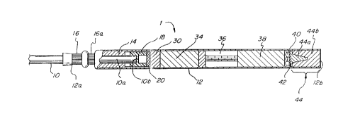
Referring now to Figure 1 there is shown one embodi-
ment of an extended range digital delay detonator 1 of the
present invention for use in detonating a downhole charge.
In the illustrated embodiment, the delay detonator is
coupled to a suitable input transmission line which com-
prises, in the illustrated case, a shock tube 10. It is
to be understood, however, that other nonelectric signal
transmission means such as a detonating cord, low energy
detonating cord, low velocity shock tube and the like may
be used. Generally, any suitable nonelectric, impulse
signal transmission means may be employed. As is well-
known to those skilled in the art, shock tube 10 comprises
hollow plastic tubing, the inside wall of which is coated
with an explosive material so that, upon ignition, a low
WO'94115169 PCT~S93/1~19
21~1911
~ .
--1 1--
energy shock wave is propagated through the tube. See,
for example, Thureson et al, U.S. Patent 4,607,573. Shock
tube 10 is fitted to a suitable housing 12 by means of an
adapter bushing 14 about which housing 12 is crimped at
5 crimps 16, 16a to secure shock tube 10 and form an envi-
ronmentally protective seal between adapter bushing 14 and
the outer surface of shock tube 10. Housing 12 has an
open end 12a which receives bushing 14 and shock tube 10,
and an opposite, closed end 12b. Housing 12 is made of an
electrically conductive material, usually aluminum, and is
preferably the size and shape of conventional blasting
caps, i.e., detonators. A segment lOa of shock tube 10
extends within housing 12 and terminates at end lOb in
close proximity to, or in abutting contact with, an anti-
static isolation cup 18.
Isolation cup 18, as best seen in Figure lA, is of atype well-known in the art and is made of a semiconductive
material, e.g., a carbon-filled polymeric material, so
that it forms a path to ground so as to dissipate any
static electricity which may travel along the interior of
shock tube 10. For example, see Gladden U.S. Patent
3,981,240. A low energy booster charge 20 is positioned
adjacent to anti-static isolation cup 18. As best seen in
Figure lA, anti-static isolation cup 18 comprises, as is
well-known in the art, a generally cylindrical body (which
is usually in the form of a truncated cone, with the larg-
er diameter positioned closer to the open end 12a of hous-
ing 12) which is divided by a thin, rupturable membrane
18b into an entry chamber 18a and an exit chamber 18c.
The end lOb of shock tube 10 (Figure 1) is received within
entry chamber 18a (shock tube 10 is not shown in Figure lA
for clarity of illustration). Exit chamber 18c provides
an air space or stand-off between the end lOb of shock
tube 10 and booster charge 20. In operation, the shock
wave traveling through shock tube lO will rupture membrane
18b and traverse the stand-off provided by exit chamber
18c and impinge upon and detonate booster charge 20.
Booster charge 20 itself comprises a booster charge
WO94/15169 PCT~S9311~19
2151911
-12-
shell 22 of cup-like configuration within which is pressed
a small quantity of primary explosive 24, such as lead
azide, which is closed by a first cushion element 26.
First cushion element 26, which is located between isola-
tion cup 18 and primary explosive 24, protects primaryexplosive 24 from pressure imposed upon it during manufac-
ture.
- A non-conductive buffer 28, which is typically 0.030
inches thick, is located between booster charge 20 and a
piezoelectric generator 30 to electrically isolate piezo-
electric generator 30 from booster charge 20.
Adapter bushing 14, isolation cup 18, first cushion
element 26, and booster charge 20 may conveniently be fit-
ted into a booster shell 32 as shown in Figure lA. The
outer surface of isolation cup 18 is in conductive contact
with the inner surface of booster shell 32 which in turn
is in conductive contact with housing 12 to provide an
electrical current path for any static electricity dis-
charged from shock tube lO. Generally, booster shell 32
is inserted into housing 12 and housing 12 is crimped to
retain booster shell 32 therein as well as to protect the
contents of housing 12 from the environment.
Referring again to Figure l, a capacitor 34 is con-
nected to piezoelectric generator 30 to receive electrical
output from generator 30 for storage. Capacitor 34 may be
a lO micro-farad unit rated at 35 volts. Its series re-
sistance is preferably low to accommodate the fast rise-
time of the l to 2 microsecond-long pulses it will receive
from piezoelectric generator 30.
A battery means 36 is positioned next to capacitor 34
and adjacent to battery means 36 is a timing module 38
next to which is located an electrically activated igniter
means 40. A second cushion element 42, which is similar
to first cushion element 26, is interposed between output
charge 44 and an electrically activated igniter means 40
for the same purpose as first cushion element 26. Output
charge 44 comprises a primary explosive 44a and a second-
ary explosive 44b, which has sufficient shock power to
WO94/1~169 2151911 PCT~S931L~19
-13-
detonate cast booster explosives, dynamite, etc., the det-
onation of which is the usual purpose to which such deto-
nators are put. Igniter means 40, which is connected to
the output of timing module 38, when energized, detonates
primary explosive 44a, which in turn detonates secondary
explosive 44b, i.e., igniter means 40 serves to detonate
output charge 44. Igniter means 40 is positioned within a
preferably non-conductive bushing (not shown) which serves
to prevent inadvertent detonation of output charge 44 by
igniter means 40 by virtue of the relatively low resis-
tivity of the bushing and its contact with housing 12.
The components contained within housing 12 are suit-
ably encased within potting compounds to protect the com-
ponents, and minimize the chances of detonation or damage
by mechanical impact or electrical signals. The fact that
housing 12 is made of aluminum or other electrically con-
ductive material, also helps to shield the internal compo-
nents against both electrical signals and mechanical
shocks that could inadvertently activate booster charge 20
or output charge 44. The electrically conductive housing
12 provides a high degree of attenuation of potentially
damaging electrical fields by forming a Faraday cage
around the electrically sensitive components. The size
and configuration of the housing 12 is, as noted above,
preferably selected to duplicate industry stAn~rd detona-
tor sizes currently in use.
In operation, the digital delay detonator l of Figure
l receives a pressure input pulse via shock tube lO which
detonates booster charge 20, the explosive output of which
is thus an amplification of the pressure input pulse de-
livered by shock tube lO. Piezoelectric generator 30 is
subjected to the energy delivered by the explosion of
booster charge 20 and converts the energy into electrical
energy. This electrical energy is stored in storage capa-
citor 34 and a part of it is used to activate the timingcircuit of timing module 38 and, after lapse of a pre-se-
lected interval, to energize igniter means 40 to detonate
output charge 44. Battery means 36 is used to supply the
WO~4/15169 21519 1 1 PCT~S93/1~19
-14-
necessary power to operate the delay timing circuitry of
timing module 38. Upon completion of its timing cycle,
the stored energy from capacitor 34 is applied to electri-
cally activated igniter means 40, thereby detonating pri-
mary explosive 44a and secondary explosive 44b. The delaydetonator 1 may thus be employed to provide a very accu-
rately controlled delay in the initiation of an explosive
charge as may be required in blasting patterns in which a
large number of charges are to be detonated in a predeter-
mined timing pattern. The electric circuit control of thedelay permits much more accurate delays than those which
are attainable by conventional pyrotechnic delays, and the
battery-powered timing means permits the selection of much
longer delays than would be attainable if the piezoelec-
tric generator 30 had to supply the power for both power-
ing the timing circuits and energizing the igniter means
40.
Referring now to Figure lB, in which parts identical
to those of the Figure 1 embodiment are identically num-
bered except for the addition of a prime indicator, analternative embodiment of the present invention comprises
a detonator 1', only a portion of which is shown in Figure
lB. In this embodiment, shock tube 10 of the Figure 1 em-
bodiment is replaced by a transmission line comprising a
low energy detonating cord 46 which is mounted within
adapter bushing 14' located at open end 12a' of housing
12' so that a portion 46a thereof is sealed within housing
12' by crimps 16', 16a~ cooperating with bushing 14' and
detonating cord 46. The energy output of detonating cord
46 is selected to be low enough not to destroy components
of delay detonator 1' so as to prevent it from function-
ing, but high enough to cause the input impulse signal
provided by the explosive output of low energy detonating
cord 46 to act, without need for amplification, directly
on piezoelectric generator 30~. Generator 30' responds to
the shock wave from low energy detonating cord 46 to gen-
erate electrical energy that is transmitted for storage in
storaqe capacitor 34'. Consequently, booster charge 20 of
WO94tl~169 PCT~S9311~19
2151911
the ~igure 1 embodiment is omitted from the embodiment of
Figure lB, as is isolation cup 18, for which there is no
need in the embodiment of Figure lB. Otherwise, the other
parts of the Figure lB embodiment, their arrangement and
operation are the same as those discussed in conjunction
with the embodiment of Figure 1 and it is therefore not
necessary to repeat the illustration and description
thereof. Generally, in the Figure lB embodiment, the
energy necessary to energize piezoelectric generator 30
is derived directly from the shock wave coming from low
energy detonating cord 46.
Figure 2 shows another embodiment of the present in-
vention as an in-line delay unit 210. In this embodiment,
housing 212 may be made of any suitable dielectric mater-
ial such as a synthetic organic polymer (plastic), for ex-
ample, polyethylene or other thermoplastic material, and
it contains the other components of the in-line delay unit
in suitable cavities formed therein. Housing 212 also
serves to receive and connect the input and output trans-
mission lines, i.e., input shock tube 214 and output shocktube 216. A suitable inlet bore (unnumbered) is formed in
housing 212 and receives and securely retains the input
shock tube 214, as described in more detail below. Input
shock tube 214 comprises a hollow plastic tube, the inner
surface of which is coated by an explosive powder layer
214a (Figure 2A). Input shock tube 214 terminates within
housing 212 adjacent to a booster charge 226.
Low energy booster detonator 218 (Figures 2 and 2A)
comprises a detonator shell 220, within which are disposed
an anti-static cup 222, a first cushion element 224, and a
booster charge 226. A transducer which, in the illustrat-
ed embodiment, comprises a piezoelectric generator 228,
and a first conductor means which, in the illustrated em-
bodiment, comprises a pair of leads 230a, 230b are mounted
within housing 212 adjacent to low energy booster detona-
tor 218. Detonator shell 220 is crimped around a bushing
231 within which input shock tube 214 is received to help
retain the end of the shock tube securely in place within
~0941l5169 2151911 PCT~S9311~19
-16-
low energy booster detonator 218. In addition, the one
hundred eighty-degree return bend configuration of the in-
let bore (Figure 2) which receives input shock tube 214
provides a strain relief which helps to hold input shock
tube 214 firmly in place within housing 212. This em-
placement of input shock tube 214 within housing 212,
which is usually carried out in factory assembly of the
device, resists the tendency of mechanical forces to dis-
lodge input shock tube 214 from housing 212.
As best seen in Figure 2A, booster charge 226 is sep-
arated from anti-static cup 222 by first cushion element
224, the function of which is to distribute, during fac-
tory assembly of booster detonator 218, the pressure of a
steel pin used to insert booster charge 226 into detonator
shell 220. This distribution of pressure reduces the
chance of detonation of booster charge 226 during the man-
ufacturing process. First cushion element 224 has a cen-
tral aperture 224a formed therein and closed by a thin,
rupturable membrane (unnumbered) to seal booster charge
226. Central aperture 224a provides a low-resistance path
to booster charge 226 for the impulse signal delivered by
input shock tube 214.
Anti-static cup 222 is in the shape of a truncated
cone with a thin, rupturable membrane 222a extending
across its midsection and against which the end of input
shock tube 214 is seated, providing an air-gap "stand-off"
between the end of input shock tube 214 and booster charge
226. Anti-static cup 222 contacts the sides of detonator
shell 220 and serves to ground any electrostatic discharge
traveling through input shock tube 214 against shell 220
to reduce the possibility of an electrostatic charge pre-
maturely detonating booster charge 226.
A buffer 225 is provided between the booster detona-
tor shell 220 and piezoelectric generator 228. Buffer 225
is a dielectric material and serves to electrically iso-
late piezoelectric generator 228 from detonator shell 220.
Piezoelectric generator 228 is thus located in close
proximity to booster charge 226 with only shell 220 and
WO94/15l69 PCT~S93/1~19
2151911
-17-
buffer 225 intervening between them. Piezoelectric gener-
ator 228 comprises multiple alternating layers of a con-
ductor and a piezoelectric ceramic wherein the metal lay-
ers are interconnected in parallel to form the output ter-
minals tnot shown) of piezoelectric qenerator 228. Leads
230a, 230b connect the output terminals of piezoelectric
generator 228 to a delay module provided in the illustrat-
ed embodiment by digital delay module 232 (Figures 2 and
2C). Referring to Figure 2C, digital delay module 232 in-
cludes an energy storage capacitor 234, a trigger circuit236, a delay circuit 238, and a programming interface
means 242 mounted thereon. Energy storage capacitor 234
is, in the illustrated embodiment, about a 3 micro-farad
unit rated at 35 volts. Its series impedance is prefer-
ably low to accommodate the fast rise time of the 1 to 2microsecond pulses generated by piezoelectric generator
228.
Referring to Figures 2 and 2B, the output of digital
delay module 232 is electrically connected by second con-
ductor means to igniter element 246 of output detonator248. In the illustrated embodiment (Figures 2 and 2B),
the second conductor r~s comprise a pair of leads 244a,
244b, the ends of which are connected by a bridge wire 245
embedded within an igniter element 246 (Figure 2B). As
best seen in Figure 2B, output detonator 248 comprises the
igniter element 246 contained within an igniter cup 247
positioned within output detonator shell 250 in close
proximity to an output charge 254. Leads 244a, 244b are
retained within output detonator shell 250 by a bushing
251 held in place by the necked-down portion (unnumbered)
of shell 250. A second cushion element 252 identical to
first cushion element 224 abuts and separates igniter ele-
ment 246 from output charge 254. Second cushion element
252 contains a central aperture 252a which serves the same
function as central aperture 224a of first cushion element
224 and is similarly closed with a thin, rupturable mem-
brane (unnumbered) to seal output charqe 254.
The end of housing 212 adjacent to output detonator
WO94/15169 PCT~S93/1~19
2151911
-18-
248 is configured to provide a plurality of output line
retainer means for retaining one or more output transmis-
sion lines in proximity to output detonator 248. In the
illustrated embodiment, these output line retainer means
are provided by a combination of output line bores 256 and
cleats 258. Output line bores 256 have entry mouths 256a
and exit mouths 256b. Cleats 258 are generally hook-shap-
ed, terminate in flexible lips 258a, and are located adja-
cent to and aligned with the exit mouths 256b of output
line bores 256. Output line bores 256 and cleats 258 thus
cooperate to provide the output line retainer means in the
illustrated embodiment. Although only two such output
line retainer means are illustrated in Figure 2, it will
be appreciated that more than two such output line retain-
er means could be provided. For example, in the illus-
- trated embodiment, four or even six such output line re-
tA;n~r means could be evenly spaced about the periphery of
housing 212.
Output shock tube 216 has a terminal end 216a which
is closed and sealed against the environment by seal 216b
which flattens and seals shock tube 216. A suitable deto-
nator cap (not shown) is crimped onto the remote end (not
shown) of shock tube 216 and may be emplaced within an ex-
plosive charge or may be utilized as a signal amplifying
and transmission cap to ignite another signal transmission
tube to which it is connected. Obviously, any suitable
length of output shock tube 216 may be employed and delay
unit 210 may remain on the surface whether output shock
tube 216 comprises a surface transmission line or a down-
hole line. Alternatively, delay unit 210 may be placedwithin a borehole, e.g., when it is used in conjunction
with an instantaneous blasting cap to provide an accurate
delay period for a downhole blasting cap. A period ta~
216c is attached near the terminal end 216a of shock tube
216 to indicate the delay period of the detonator cap (not
shown) attached to the remote end (not shown) of shock
tube 216. In the illustrated embodiment, the legend ~Per-
iod Zero" on period tag 216c indicates that the detonator
WOg4/l5169 2151911 PCT~S9311~19
--19--
cap attached to the remote end of shock tube 216 has no
delay period, i.e., it is a zero period or instantaneous
detonating cap. Obviously, depending on the design of a
particular blasting pattern, the detonator cap at the re-
mote end of shock tube 216 may, if desired, have an elec-
tronically controlled time delay period and such would be
reflected in period tag 216c. A digital delay detonator
cap of the type described in U.S. Patent 5,173,569 would
provide an accurate cap delay period.
10Shock tube 216 is easily and securely attached to
housing 212 by bending the tube back on itself a short
distance away from terminal end 216a so as to form a loop
or bight in shock tube 216, and forcing the bight of the
tube upwardly into entry mouth 256a of bore 256 and out
15through exit mouth 256b to protrude beyond mouth 256b.
The bight is advanced to protrude a distance sufficient to
enable folding over of the shock tube to bring the bight
thereof beneath the associated cleat 258 in the vicinity
of the lip 258a thereof. The overlapping lengths of the
shock tube are then pulled downwardly in the direction of
the unnumbered arrow in Figure 2, to pull the bight of the
tube upwardly past flexible lip 258a and thus seat the
looped shock tube 216 firmly within cleat 258 as shown in
Figure 2. Additional output transmission tubes may be
secured to the other output line retainer mean(s) of hous-
ing 212 in the same manner. The proximity of shock tube
216 (and of any other output transmission lines similarly
attached to housing 212) to output detonator 248 assures
that the detonation of output detonator 248 will initiate
an output signal in the connected output transmission
lines. The combination of output detonator 248 and ignit-
er element 246 provides an electrically detonatable output
charge.
A programming interface means 242, which may comprise
any suitable electrical, optical or other programming in-
terface means is programmable from exteriorly of housing
212 and may be connected to digital delay module 232 by
any suitable means represented by interface connector 262.
~094/l5169 PCT~S93/1~19
2151911
-20-
A programming window 268 is formed in housing 212 against
which a suitable programming interface means 242 (not
shown), such as a hand-held programmer, may be placed to
carry out programming of delay unit 210 to provide a se-
lected delay period for it. A guide-ridge 268a is formed
about the periphery of programming window 268 to guide
placement and retention of the programming interface means
242 in proper alignment with programming window 268.
Interface connector 262 may comprise any suitable
connector means, e.g., soldered electrical wires, which,
in the illustrated embodiment, serve to connect program-
ming interface means 242 to digital delay module 232 to
enable the entry of a specific time delay into delay mod-
ule 232. The power necessary to perform this function and
the programming signal can be transferred by induction in
a pick-up coil comprising part of programming interface
means 242, in a well-known manner. In this way, program-
ming interface means 242 need not have any external pins
or metallic conductive means requiring one or more physi-
cal openings in housing 212. This helps to assure the in-
tegrity of housing 212 and the contents thereof against
environmental and stray electric field effects.
If the programming of digital delay module 232 is to
be performed via an optical path, a small battery having a
long shelf life, such as a lithium battery, is provided to
supply the power necessary for performing the programming
function. The voltage and capacity of the battery is cho-
sen to ensure that the energy available from the battery
is not sufficient to trigger igniter element 246 in case
of a malfunction.
In a typical embodiment, housing 212 is made of a
non-conductive polymer that shields the internal compo-
nents against both electrical signals and mechanical
shocks that could inadvertently activate low energy boost-
er detonator 218 or output detonator 248. To increase
shielding effectiveness against electrical disturbances,
conductive members (not shown) may be encased within the
walls of housing 212 to provide a high degree of attenua-
W(~94/15169 PCTJUS93/12319
21~1911
--21--
tion of magnetic or electrical fields thereby protecting
the internal circuitry, including the programming cir-
cuits, by forming a Faraday cage around the electrically
sensitive components. Alternatively, housing 212 may com-
5 prise a semi-conductive material to provide shielding for
the circuitry components.
Assembly of the components may be carried out by en-
capsulating the components with potting compound within
suitable recesses formed in housing 212, which may be gen-
10 erally cylindrical in configuration. Preferably, the in-
put transmission line such as shock tube 214 will be fac-
tory-installed and sealed within housing 212. The delay
unit of the present invention may thus be provided with
only a suitable length of shock tube 214 (or other suita-
15 ble input transmission line) attached thereto. In suchcase, the connections to output transmission tubes, such
as illustrated output shock tube 216, may be made in the
field as reguired. Alternatively, both input and output
transmission lines may be factory-installed or field-as-
20 sembled.
A cover (not shown in the drawings) may be providedfor housing 212 to cover and seal the installed compo-
nents. As a final step in the assembly of housing 212,
the cover may be secured in place by integral clips, ul-
25 trasonic welding, solvent bonding, ultrasonic staking, oran adhesive in order to provide a moisture-tight enclosure
protected from the environment.
The operation of the delay unit 210 of Figures 2 and
2C is described with reference to Figures 2, 2C and 2E,
30 the latter Figure showing details of one embodiment of the
circuitry of delay module 232. Ignition of the input
shock tube 214 delivers an impulse signal to low energy
booster detonator 218, where it ruptures the membrane of
anti-static cup 222 and first cushion element 224 to im-
35 pact upon booster charge 226 and detonate it. Piezoelec-
tric generator 228 converts the shock energy delivered to
it by the detonation of booster charge 226 into electrical
energy which is delivered to digital delay module 232 via
WO94/15169 PC~S93/1~19
21Sl91l
-22-
leads 230a, 230b. Digital delay module 232 stores the
electrical energy delivered to it from piezoelectric gen-
erator 228 in capacitor 234. In the illustrated embodi-
ment, piezoelectric generator 228 and energy storage ca-
pacitor 234, respectively, comprise the transducer and en-
ergy storage means which together comprise the signal con-
version means of the present invention. The electrical
energy stored in capacitor 234 is used in one embodiment
for two purposes: the powering of the electronic timing of
the digital deiay module 232 and, after the preset time
delay, the ignition of igniter element 246. More specifi-
cally, when the voltage of the el~ectrical energy stored in
capacitor 234 is above a selected threshhold, the logic
and timer portion of the delay module 232 (Figure 2C) is
energized.
Referring to Figure 2E, the first electric signal
generated by piezoelectric generator 228 is transmitted
through steering diode 266 to capacitor 234, which stores
the electrical energy. When a predetermined minimum volt-
age is reached on capacitor 234, voltage regulator 277 is
activated to apply a portion only of the power generated
by piezoelectric generator 228 to the timing circuits of
oscillator 278, counter 280, and power-on reset circuit
282. A silicon controlled rectifier ("SCR") 284 is acti-
vated by counter 280 at the conclusion of the timing in-
terval, thereby supplying the remaining energy in capac-
itor 234 to the second conductor means provided, in the
illustrated embodiment, by leads 244a, 244b.
During operation of the circuit of Figure 2E, the
power-on reset circuit 282 preloads the counter 280 with
count information from interface connector 262 (~igures 2
and 2C) or, in an embodiment of the invention (not illus-
trated) which does not include a programming interface
means such as programming interface means 242, preloads
the counter with an initial preset count value. This pre-
loading occurs at the time capacitor 234 receives the
electrical signal from piezoelectric generator 228.
Concurrently, oscillator 2?8 starts generating pulses (or
WO~4/1~169 PCT~S9311~19
2151911
'
-23-
cycles) that are counted by counter 280. As the counter
280, activated by the pulses from oscillator 278, reaches
a pre-selected count as, for example, 1, the preprogrammed
delay period expires and an activation signal is sent to
SCR 284. The activation signal puts SCR 284 in a conduct-
ing state which allows it to conduct the electrical energy
in capacitor 234 to leads 244a, 244b and bridge wire 245
which, in the illustrated embodiment, provide the second
conductor ~ns which serve to detonate igniter element
246 and thereby detonate output charge 254 (Figure 2B)
which, in turn, ignites the shock tube(s) 2l6 retained in
proximity to detonator 248.
The arrival at SCR 284 from capacitor 234 of the en-
ergy needed to detonate output charge 254 is seen to be
delayed by an interval essentially equal to the time re-
quired for the counter 280 to count the pulses from oscil-
lator 278 from the initially preset amount from power-on
reset circuit 282, to some value, for example, l.
In other embodiments of the invention, a battery may
be included in the circuit to supply energy for program-
ming the time delay. In yet another embodiment, the bat-
tery energy may also be used not only for programming the
time delay, but also for powering the delay circuits.
However, in all embodiments of the invention, ignition of
the output charge (item 254 in the embodiment illustrated
in Figure 2B) is powered by energy emitted from the trans-
ducer (piezoelectric generator 228 in the embodiment illu-
strated in Figure 2A) and not by battery or other stored
energy sources. The battery or other stored energy source
utilized is of insufficient power to detonate the output
charge. This provides a safety factor because the piezo-
electric generator is designed to be actuated substantial-
ly only by the impulse signal imposed upon it by detona-
tion of the booster charge (item 226 in the embodiment il-
lustrated in Figure 2A) or the detonating cord, describedbelow in connection with the embodiment of Figure 2D.
Thus, the transducer (e.g., the piezoelectric generator
228) is of sufficiently low sensitivity that mechanical
W094/15169 2151911 PCT~S93/1~19
,_
-24-
shocks or vibration imposed upon it by rough handling, be-
ing dropped or impacted in normal or rough usage, or by
nearby explosions, e.g., in an adjacent borehole, will not
cause the transducer to be activated. Thus, the transduc-
er will generate electric power sufficient to ignite theigniter element (item 246 in the embodiment illustrated in
Figure 2B) and thereby ignite the output charge (item 254
in the emhodiment of Figure 2B) to generate the outgoing
signal substantially only by the input impulse signal or
the amplification thereof by the booster charge (item 226
in the embodiment of Figure 2A).
Thus, in cases where a battery or other suitable
stored energy source is provided, instead of using the
power derived from the piezoelectric generator, e.g.,
piezoelectric generator 228 of the illustrated embodi-
ments, for both the timing and ignition of the output
charge (output charge 254 in the illustrated embodiments)
the delay circuits are powered by a source, e.g., a bat-
tery, connected therethrough through a silicon controlled
rectifier (SCR) switch which is activated by a signal de-
rived from the energy output of the piezoelectric genera-
tor. An embodiment of the invention illustrating the
utilization of battery power for both programming the time
delay and powering the delay circuits is illustrated in
Figure 3. The utilization of battery power enables the
provision of a much longer delay period than that which
could be attained if the piezoelectric generator were the
sole source of power.
Further details of the operation of the present in-
vention are illustrated in Figure 2C which diagrammatical-
ly shows input shock tube 214 for delivering a pressure
input pulse to low energy booster detonator 218 which de-
tonates to provide the amplified signal used to generate a
pressure pulse on piezoelectric generator 228. Energy
storage capacitor 234, trigger circuit 236 and delay cir-
cuit 238 are part of digital delay module 232. Piezoelec-
tric generator 228 generates the first electric signal
pulse in response to the pressure imposed on it from low
WO'94115169 2151911 PCT~S9311~19
-25-
energy booster detonator 218. This first electric signal
is stored in an energy storage capacitor 234 to be subse-
quently used by trigger circuit 236 and delay circuit 238.
Delay circuit 238 activates trigger circuit 236 after the
time interval programmed into delay circuit 238 has elaps-
ed. Trigger circuit 236 allows electrical energy stored
in energy storage capacitor 234 to flow as a second elec-
trical signal to igniter element 246, thereby triggering
output charge 254 to qenerate a pressure output pulse
large enough to initiate one or more output transmission
lines such as shock tube(s) 216 which are retained in
close proximity to output charge 254.
Optionally, delay circuit 238 communicates through
interface connector 262 and programming interface means
242 with any suitable external means (not shown) placed
against programming window 268 and oriented thereagainst
by guide-ridge 268a (Figures 2 and 2C). The signals from
the external programmer means are encoded by any suitable
well-known techniques to both power and pass delay infor-
mation to delay circuit 238 via interface means 242 and
interface connector 262. By way of illustration, an in-
fra-red emitter 260a and receiver 260b are shown in Figure
2 as the means to provide communication between the exter-
nal programmer means and interface means 242.
Figure 2D shows another embodiment of the present in-
vention in which items similar to those of the embodiment
of Figures 2 and 2C are identically numbered to those of
Figure 2 but with the addition of a prime indicator.
Identical components are identically numbered. In the em-
bodiment of Figure 2D, the input transmission line con-
nected to delay unit 2l0' is provided by a low energy de-
tonating cord 2 14 ', which is used in lieu of input shock
tube 214 and booster charge 226 of the embodiment of Fig-
ures 2 and 2C. In the illustrated embodiment of Figure
2D, detonating cord 214' is mounted in housing 212 in the
same manner as shock tube 214 of the Figure 2 embodiment,
but terminates in opposite-facing proximity to piezoelec-
tric generator 228 within a chamber 215 defined by detona-
WO 94/15169 2151911 PCTtUS93112319
-26-
tor shell 220'. The impulse input signal required to ac-
tivate the piezoelectric generator is provided in this em-
bodiment directly by low energy detonating cord 214'. The
low energy detonating cord has a solid explosive core
214a' of sufficiently low explosive power to ensure the
preservation of the integrity of the housing 212 of the
in-line delay unit 210'. Nonetheless, detonating cord
214' has sufficient explosive power to directly excite the
piezoelectric generator 228 to produce electrical energy
sufficient to generate the electric signal needed to deto-
nate the output charge (not shown in Figure 2D). Piezo-
electric generator 228 responds to the input impulse sig-
nal provided by the explosion shock wave generated by
detonation of low energy detonating cord 214' by generat-
ing electrical energy that is stored in energy storage
capacitor 234 (not shown in Figure 2D). All the compo-
nents of the embodiment of Figure 2D other than as specif-
ically set forth above, are identical to those illustrated
in Figure 2 and function in exactly the same manner.
Therefore, it is not necessary to illustrate them in Fig-
ure 2D or to repeat the description of their function.
It will be appreciated that the above-described em-
bodiment of the present invention thus provides an accu-
rate time delay between an impulse input signal (flame
front, pressure wave, explosion, etc.), i.e., a non-elec-
tric signal, carried by an input transmission line and an
output impulse signal transmitted by one or more output
transmission lines to, e.g., each borehole in a group of
multiple boreholes. In addition, the signal line connect-
or embodiment described above provides for a field pro-
grammable delay detonator, adjustable in small time incre-
ments, thereby requiring only a single type of in-line de-
lay unit to be kept in stock and used for the implementa-
tion of different in-line delays at a blasting site.
Figure 3 details schematically an example of an elec-
tric timing circuit suitable for use in timing module 38
of the embodiment of Figure l or digital delay moduIe 232
of the embodiment of Figure 2, with which the optional in-
WO'94/15169 21~191 1 PCT~S93/1~19
-27-
terface connector 262 may be employed, as described above.
Elements of Figure 3 which are also illustrated in Figure
1 are identically numbered in both Figures, although it
will be understood that corresponding elements can also
generally be found in the embodiment of Figures 2-2D.
Piezoelectric generator 30 generates electrical current
when it is pressurized as described above, e.g., by deto-
nation of booster charge 20 (Figure 1) or low energy deto-
nating cord 46 (Figure lB). The output energy from gener-
ator 30 passes through steering diode 48 and is stored instorage capacitor 34. The voltage reached by capacitor 34
is divided by resistors 52 and 54 to activate silicon con-
trolled rectifier ~"SCR") 56. Once activated, SCR 56
causes the power from battery means 36 to be applied to
the timing circuits comprising oscillator 60, programmable
counter 62, and power-on reset ("POR") circuit 64. At the
conclusion of the preset timing interval, SCR 66 is acti-
vated by programmable counter 62 thereby releasing the
electrical energy stored in capacitor 34 to flow to igni-
ter means 40.
During operation of the timing circuit of Figure 3,the POR circuit 64 preloads the programmable counter 62
with count information, setting the counter 62 with an in-
itial preset count value. This preloading occurs upon the
activation of SCR 56, i.e., at the time capacitor 34 re-
ceives the electrical input from piezoelectric generator
30. Concurrently, oscillator 60 starts generating pulses
(or cycles) that are counted by counter 62. As the count-
er 62, activated by the pulses from oscillator 60, reaches
a preselected count, as for example 1, the preprogrammed
delay period expires and an activation signal is sent to
SCR 66. The activation signal puts SCR 66 in a conducting
state which allows SCR 66 to conduct the electrical enerqy
in capacitor 34 to igniter means 40 via lead 40a, bridge
wire 41, and lead 4Ob, thereby detonating output charge
44. (Output charge 44 is not shown in Figure 3 but is
shown in Figure 1.)
The arrival of the energy from storage capacitor 34
WO94/15169 2 1 5 1911 PC~S93/1~19
~_ -28-
at igniter means 40 and the consequent detonation of out-
put charge 44 is therefore delayed by an interval essen-
tially equal to the time required for the programmable
counter 62 to count the pulses from oscillator 60 from the
initial preset amount established by POR circuit 64 to
some value, such as, for example, 1. This arrangement
provides an accurate time delay means for a non-electric,
pressure-type signal, i.e., an impulse input signal pro-
vided to the delay detonator of the present invention by a
suitable transmission line such as shock tube 10 (Figure
1) or detonating cord 46 (Figure lB). The programmed de-
lay will have an exceedingly small unit-to-unit variance.
Consequently, the variance in time delay detonation of
each borehole in a group of multiple boreholes will corre-
spondingly be exceedingly small. The programmability ofthe circuitry allows a single type or model of delay deto-
nator in accordance with the present invention to be used
for the implementation of different delays. Thus, a sin-
gle stock item may be used to provide an entire series of
highly accurate detonators of selected delay periods.
Figure 4 is a more detailed version of the circuitry
of Figure 3, in which some details of typical circuitry
suitable for oscillator 60, programmable counter 62 and
POR circuit 64 are shown. Elements of Figure 4 which are
illustrated in Figure 3 are identically numbered in both
Figures.
As described above in connection with Figure 3, upon
activation of the piezoelectric generator 30, current
flows through the steering diode 48 to charge the storage
capacitor 34 and the voltage divider formed by resistor 52
and resistor 54 provides a trigger signal to SCR 56, which
causes the power from battery means 36 to be applied to
the timing circuitry. Referring to Figure 4, programmable
counter 62 is seen to comprise a first counter 62a, and a
second counter 62b, both of which typically may be well-
known monolithic counters such as an industry standard
part number 40193. Figure 4 shows standard nomenclature
to indicate various parts and connectors, viz., VDD =
WO94/15169 PCT~S93/1~19
215191~
-29-
power and VSS = ground. The POR circuit 64 includes re-
sistor 110, capacitor 111, Schmidtt-Trigger buffer 133,
and inverter 112. Alternatively, an oscillator circuit
could be made up of a crystal oscillator, as is well-known
in the art. In any case, upon application of input volt-
age to it, POR circuit 64 preloads first counter 62a.
Once the voltaqe from the battery means 36 has increased
beyond a threshold setting, first counter 62a begins de-
crementing with each input pulse from the oscillator 60.
As the counter decrements past zero, the output to SCR 66
is activated and the energy in storage capacitor 34 is ap-
plied to the igniter means 40.
There are many known methods of accomplishing the de-
lay aspect of the operation and Figure 4 shows one exem-
plary circuit which will accomplish the timing task. Thecircuit of Figure 4 may be comprised of commercially
available components and the specific embodiment of the
invention illustrated incorporates items such as counters
62a and 62b, and the components numbered 107 through 133
onto a single complementary metal oxide semiconductor in-
tegrated circuit ("I.C.") 106.
The circuit of oscillator 60 is comprised of timing
resistor 107, timing capacitor 108, and a commercially
available LM 555 timer 109. The programming circuitry
utilizes steering diodes 114-117, and 123-126, as well as
fuses 118-121 and 127-130.
Once SCR 56 is triggered on as described above, power
is applied to the delay circuitry from battery means 36.
Capacitor 111 of POR circuit 64 is slowly charged through
resistor 110 by the voltage apparent at node 135. Once
the voltage at capacitor 111 has attained a level of two-
thirds of the voltage of node 135, buffer 133 switches the
signal of node 137 from a low t~o a high state. While node
137 is held low, the preset inputs to the counters are ac-
tive, causing the signals apparent at the respective sets
of inputs Pl to P4 to be loaded into the counters 62a and
62b. At this point, the inhibit signal node 138 is held
high to prevent the oscillator 60 from functioning. Once
WO94/15169 PCT~S93/1~19
2151911
~_ -30-
node 137 switches from low to high, both the oscillator 60
and counters 62a, 62b are enabled and begin functioning.
The output of the oscillator 60 at node 139 directly
decrements counter 62a from its preset value. As counter
62a decrements past zero, node 140 is pulsed low and trig-
gers second counter 62b to decrement one count. Operation
continues in this manner until counter 62b decrements past
zero. At this time, the borrow output from counter 62b is
switched low, gets inverted to a high by inverter 131 at
node 141, and activates SCR 66, causing the energy in
storage capacitor 34 to be applied to igniter means 40 as
described above.
Proqramming of the circuit illustrated in Figure 4 is
accomplished by applying a voltage to pins 6 to 13. This
voltage application produces a current flow through fuses
118-121 and 127-130. Pin 3 connected to node 139 is pro-
vided to allow measurement of the actual oscillator fre-
quency. Through the use of this measurement, it is possi-
ble to program extremely precise delay intervals without
the complications of precision trimming the oscillator 60
to a specific frequency.
Generally, fuses 118-121 proqram first counter 62a to
divide by an integer up to 16, as is well-known in the
art. Similarly, fuses 127-130 program second counter 62b.
In this configuration, first counter 62a will output a
signal after a number of cycles have been received from
the LM 555 timer 109 of oscillator 60, i.e., a signal will
be output when the counter has counted down by the number
of preprogrammed cycles or pulses received from oscillator
60. Second counter 62b receives its input from the output
of first counter 62a. The input to second counter 62b
will be essentially divided as programmed by fuses 118-
121. The state of these fuses determines the counting
program of counters 62a and 62b, as is well-known in the
art.
During counter operation, the output pulses from os-
cillator 60 will be divided by both first counter 62a and
second counter 62b as programmed by fuses 118-121 and
WO'94/15169 PCT~S93/1~19
21Sl91l
.~....
-31-
127-130. For example, if first counter 62a is programmed
to count down (or divide) from 6, and second counter 62b
is programmed to count down from 8, then SCR 66 will be
activated after 48 pulses have been generated by oscilla-
tor 60 and counted down by both counters.
While a two-stage counter circuit (counter 62a and
62b) is shown in Figure 4, additional stages may be cas-
caded as is well-known in the art for longer time delays
or improved programming resolution.
The programming section of Figure 4 is simple in that
parallel connections are used and the fuses are all burned
at the same time. While this produces no difficulties for
factory programming of the units, the number of external
connections required makes programming in the field pro-
hibitive. If field programmability of the delay detonator
is desired, additional programming circuitry may be uti-
lized to reduce the number of external connections to a
point where programming in a field environment is feasi-
ble. An example of such additional circuitry is schemati-
cally illustrated in Figure 5, wherein a dual, four-stage
static shift register, stAn~Ard part number 4015, is illu-
strated and st~n~rd nomenclature is shown to indicate
various parts and connectors, viz., VDD = power, VSS =
ground, CKA and CKB = clocks for segments A and B respec-
tively, DA and DB = data for segments A and B respective-
ly, and QlA-Q4A and QlB-Q4B = data outputs for segments A
and B respectively. The illustrated SCRs 202 through 209
are used to select the appropriate fuses (shown in Figure
4) for programming. Activation of these SCRs is performed
by loadinq the required data lines serially into shift re-
gister 201. A commercially available 4015 shift register
is shown schematically in Figure 5 but a preferred embodi-
ment would include these functions on the I.C. 85 of Fig-
ure 4. Once the required programming SCRs are active, a
high signal is applied to SCR 210. This high signal ap-
plies the programming voltage through the selected SCRs
(202-209) and burns out the associated fuse illustrated in
Figure 4. By utilizing the circuit of Figure 5, the re-
WO~4/15169 PCT~S93/1~19
2151911
-32-
quired number of pins for programming is made independent
of the number of stages used for the counter.
While any suitable transducer may be employed in the
practice of the present invention, an effective type of
piezoelectric generator is schematically illustrated in
Figures 6, 7 and 8, in which elements which are also shown
in Figures l and lA are numbered identically in both sets
of Figures.
The piezoelectric generator 30 comprises a piezocera-
mic material stack 50 comprised of a stack of multiplelayers 5l of thin piezoceramic material. The stack 50 is
supported on a suitable plastic (synthetic organic poly-
meric material) housing 53, through which terminals 68A
and 68b (Figure 7) extend. The output energy from the
booster charge 20 impinges substantially directly upon a
load distributing disc 70 (not shown in Figures l or lA),
which in turn evenly transmits the energy from the booster
charge 20 to the multiple layers 51 of suitable thin piez-
oceramic material which comprise one embodiment of the
stack 50 of piezoelectric generator 30. As best seen in
the schematic representation of Figure 8, the piezoceramic
material layers 5l are stacked in vertical layers with op-
posite faces of each layer connected in parallel through
the use of electrode layers 72a and 72b interposed between
each layer or element 5l. In one embodiment, the piezo-
electric generator of the present invention uses 84 active
layers, each approximately 20 microns thick, with discrete
positive and negative electrodes as marked on Figure 8
formed from the inner connections. This construction pro-
vides output energy levels much greater than those whichcan be obtained from an otherwise comparable monolithic
piezoceramic structure.
Referring to Figures 6, 7 and 8 jointly, the plastic
housinq 53 and load distributing disc 70 contribute, in a
preferred structure of the present invention, to obtaininq
the maximum benefit from the output shock wave of the
booster charge 20 and the physical pressure attendant
thereto. The stack 50 of piezoelectric generator 30 is
WO3411~169 PCT~S93/1~19
21Sl91l
-33-
mounted to a smooth, flat and hard surface 53a of plastic
housing 53 (Figure 7). Surface 53a is substantially par-
allel to the shock wave front generated by detonation of
booster charge 20 and perpendicular to the direction of
shock wave travel. To further obtain maxium benefit from
the output shock wave of the booster charge 20, the load
distributing disc 70 is disposed substantially parallel to
and between the output end of the booster charge 20 and
the input face of the piezoelectric generator 30 to evenly
transmit and distribute the output shock wave energy of
the booster charge 20 to the piezoelectric generator 30.
This arrangement also helps to prevent premature shatter-
ing of the piezoelectric generator 30 which would render
it inoperable. Terminals 68a and 68b are electrically
connected to electrode layers 72a and 72b to establish the
desired electrical connection to the timing module 38.
Plastic housing 53 and load distributing disc 70 also
serve to insulate piezoelectric generator 30 against un-
intended and random mech~n;cal forces, any electrical
charges, etc., and serves to help maintain the piezoelec-
tric generator in the desired position.
Although the present invention has been shown and de-
scribed with respect to preferred embodiments, various
changes and other modifications which are obvious to per-
sons skilled in the art to which the invention pertainsare deemed to lie within the spirit and scope of the in-
vention. For example, the input pressure signal need not
be limited to shock tubes but can be derived from other
non-electric, pressure transmission devices such as low
energy detonating cord, or low velocity shock tube, or any
other source of shock energy that can be made to reach the
piezoelectric generator to produce the input pressure
needed to output the required electrical signal. Further-
more, the timing circuit described can also comprise other
ways of timing an interval as is well-known in the art.
While the invention has been described in detail with
respect to preferred embodiments thereof, it is to be un-
WO94/15169 PCT~S93112319
~4151911
derstood that upon a reading of the foregoing description,variations to the specific embodiments disclosed may occur
to those skilled in the art and it is intended to include
such variations within the scope of the appended claims.