Note: Descriptions are shown in the official language in which they were submitted.
2152109
-
U:UKk~ MODE DaIVI3R FOR D1Y~ BIJS
FTRT.n OF ;T~7T~ I ~V~-~L1ON
This invention relates to circuits that can be used to drive
differential backplane buses and more particularly to circuits which drive
these buses in a way such that the difference in voltage on the bus
represents a digital binary value.
D~er~TPTION OF TS~ ~T.~T~3D ART
10A typical prior art differential bus for ECL (emitter coupled
- logic) consists of differential leads that must be isolated from the bus
when a master is not using the bus. ECL achieves this isolation by using a
third output state of the driver which is a high impedance isolation state.
When using ECL type signal levels, both signal paths are biased equally to
an appropriate ECL termination voltage which is normally 2 volts below the
top rail voltage. With this termination bias arran~e~ t, an nnh~l~nced
signal wave will propagate when going into or out of the high impedance
isolation condition. Since the first bit that is driven after coming out of
the isolation condition propagates as an nnhllinced wave, its electrical
characteristics are significantly poorer than a differentially driven
signal. This causes a constraint that limits the speed of the bus.
Another difficulty with ECL is that- it does not provide a
boolean function on the bus which can be used for arbitration and control
functions. If one bus master asserts a logic zero while another bus master
asserts a logic one in ECL, the signal on the bus is undefined, and the
output is simply noise. Single ended buses such as TTL do provide a boolean
function but as pointed out hereinabove such buses suffer from high power or
lack of noise immunity.
Still another difficulty with commonly used interface
technologies, such as TTL, PECL, ECL, BTL, and GTL, is that they use voltage
mode bus drivers which drive the bus to certain predetermined voltages to
represent the logic states. As the speed requirement in buses for
telecnmm-~ln;cations applications increases, the time slot period for one bit
approaches the amount of time that a signal edge takes to traverse a
fraction of the backplane length. As a result, the last digital bit from
one of the masters can be passing a second master on the bus when it is time
for that second master to begin transmission. If the second master sees the
2152109
digital value on the bus which it intends to transmit, the voltage mode bus
driver from that second master will not contribute to the bus until that
last bit from the first master is ended. This causes the bus driver in the
second master to produce a first digital bit with less than the full time
slot period, and this short digital bit typically cannot be properly
received.
The problems pointed out herein above with respect to prior art
backplane buses are solved in accordance with the invention described in my
copending application entitled "Backplane Bus For Differential Signals"
which has been filed on the same date herewith. In this invention a
~ backplane bus for differential signals is provided wherein two signal leads
are present for each of the digital bits to be transmitted on the bus. The
two signal leads for each one of the digital bits are terminated with their
characteristic impedances by a network at each end of the transmission
paths, and these networks bias the two signal leads with a different DC
voltage on each one of the two leads. This normally present DC voltage
difference between the two leads represents one of the two binary digital
states. Digital information is coupled to the two leads of the bus for each
digital bit through a current mode bus driver which couples current into one
of the two leads and out of the other one of the two leads in response to
the other binary digital state, thereby changing the difference in voltage
between the two leads. Accordingly, the current mode bus driver for this
new advantageous bus must be isolated from the bus for one of the two binary
digital states and must couple current into one of the two leads of the bus
and out of the other one of the two leads-of the bus for the other one of
the two binary digital states.
2152109
SnMU~Y OF T~R I NV~lON
The present invention involves a current mode bus driver which
is useful in coupling an input digital signal to a differential voltage bus
of the type which is biased with a voltage difference representing one
binary type. In accordance with the present invention, a current source is
connected to one lead of the bus and a current sink is connected to the
other lead of the bus when the input digital signal represents the other
binary type, thereby changing the voltage difference on the bus to represent
that other binary type. When the input digital signal represents the first-
mentioned binary type, the ~uLLent source and are ~LLent sink are connected
together and isolated from the bus.
It is an aspect of the present invention that the current source
and current sink are switchably connected together or to the bus by MOSFETs
whose gates are driven by unique buffer driver circuits each of which uses
an NPN transistor to drive the gate of a MOSFET with a high peak current
- thereby ensuring rapid switching of voltages on the bus.
It is another aspect of the present invention that the current
source and current sink are provided by a unique combination of MOSFETs and
NPN transistors thereby permitting the differential voltages on the bus to
swing around a lower voltage than would otherwise be permitted.
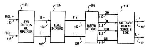
R~TRF DRC~TPTIQN OF T~R DRAWING
Figure 1 is a block diagram of the entire current mode bus
- -25 driver which illustrates how figures 2-5 must be placed in order to obtain
a complete schematic diagram of the circuit;
Figure 2 is a schematic diagram of the level shifters and
amplifier used to process input PEC~ signalsi
Figure 3 is a schematic diagram of level shifters used to
further shift the level of signals at the output of the circuit of Fig. 2;
Figure 4 is a schematic diagram of buffer driver circuits used
to convert the level shifted signals from Fig. 3 into signals with
sufficient peak current to drive the gates of the MOSFET switches in Fig. 5;
and
Figure 5 is a schematic diagram of a current source and current
sink used to drive the MOSFET switches which either connect the current
source and current sink to the leads of the bus or connect the current
2152109
source to the current sink in isolation from the bus.
DESCRIPTION OF T~E p~ n EpsoDrMvNT
A current mode bus driver of the type useful in coupling pseudo
or positive emitter coupled logic (PECL) signals to the D2L backplane bus
disclosed in my above-identified copending application is shown in Fig. 1.
As indicated in Fig. 1, the circuits of figures 2, 3, 4 and 5 are connected
in tandem as shown to provide an apparatus which causes the PECL
differential voltage signals to operate the signal leads L+ and L- of the
3US. The operation of the entire apparatus will be more readily understood
after reading the following detailed description of the operation of the
individual circuits of Figs. 2-5.
As pointed out in my cop~n~;ng patent application, the ~ss~n~
characteristic of the current mode bus driver of Fig. 1 is to supply a
current source to one signal lead of the bus and a current sink to the other
signal lead of the bus for an input binary value of one type, and to isolate
the current source and sink from the bus for an input binary value of the
other type. The part of the apparatus in Fig. 1 which accomplishes this
task is present in the circuit of Fig. 5, and it is therefore most useful in
obta;n;ng an understin~ing of the present invention to discuss this circuit
first. The L. ;ning circuits of Figs. 2-4 simply modify the voltage levels
of the PECL signals at the input of the apparatus and increase their power
level to the point where they can effectively switch the current source and
sink at a high rate of speed with digital signals on lines 110-113 at the
- - 25 input of block 114 in Fig. 1.
In Fig. 5, a fixed reference potential, Vc8, is coupled to the
base of an NPN transistor 501 whose emitter is connected through a resistor
502 to ground thereby establishing a reference current into the collector of
transistor 501. The collector of transistor 501 is connected to, and the
reference current is drawn from, the drain of a metal oxide semiconductor
field effect transistor (MOSFET) 503 of the p-~h lnn~l ~nh~nr- - type. The
gate of MOSFET 503 is also connected to its drain, and its source electrode
is connected to a potential source 515 of V., which in the present embo~ n~
is equal to 5 volts. A MOSFET 504 of the p-channel ~nh~nc~nt type also
3s has its source electrode connected to the potential source of V~, and has its
gate electrode connected to the gate electrode of MOSFET 503. As will be
appreciated by those skilled in the art, MOSFET's 503 and 504 are connected
2152109
in a current mirror arrangement whereby the current out of the drain of
MOSFET 504 is related to the current out of the drain of MOSFET 503 by the
ratio of the widths of the gate electrodes. Since the current out of the
drain of MOSFET 503 is only used as a reference current, it is set, by
choosing the value of resistor 502, equal to about one-fourth the current
out of the drain of MOSFET 504 in order to reduce the amount of power
consumed. In the present embodiment, the desired current is equal to about
10 ma., and the reference current is equal to about 2.5 ma. Accordingly,
the width of the gate electrode of MOSFET 504 is chosen to be equal to four
times the width of the gate electrode of MOSFET 503.
A MOSFET 508 of the p-channel enhancement type also has its
source electrode connected to the potential source, V., and its gate
electrode connected to the gate electrode of MOSFET 503 with a gate
electrode width equal to that of MOSFET 504. As a result a mirrored current
of about 10 ma. is available from the drain of MOSFET 508 on line 516. This
is the current which in selected cases will be switched in a manner to be
described hereinafter onto signal lead 102 (L+) of the BUS.
To provide a current sink, the mirrored current out of the drain
of MOSFET 504 is coupled into the collector electrode of an NPN transistor
505. The collector of transistor 505 is connected to its base electrode
through the base-emitter junction of an NPN transistor 507, the collector
electrode of which is connected to the potential source 515 of V~. The
emitter of transistor 505 is connected through a resistor 506 to ground. An
NPN transistor 509 with an emitter area equal to that of transistor 505 has
-- ~ 25 its base electrode connected to the base of transistor 505, and its emitter
electrode connected to ground through a resistor 510 subst inti~lly equal in
value to resistor 506. Those skilled in the art will recognize the circuit
arrangement provided by transistors 505, 507 and 509 as a current mirror
which provides a current sink at the collector of transistor 509 for a
current, I-, on line 517 equal in value to the current being driven into the
collector of transistor 505. As pointed out herein above, this current into
the collector of transistor 505 is equal in value to the current, I+, on
line 516, and therefor the magnitude of current source of I+ is
substantially equal to the magnitude current sink of I-.
The current, I+, on line 516 is connected to the drain of an n-
rh~nn~l ~nh~nc~m~nt type MOSFET 510 whose source is connected to signal lead
102 (L+) and whose gate is connected to receive a digital signal (COH)
2152IO9
present on line 1}0. When the gate of MOSFET 510 is hard driven with a
sufficiently high positive pot~nt;~l, the current, I+, is coupled through to
signal lead 102 (L+) of the BUS. Similarly, the current, I-, on line 517 is
connected to the source of an n-channel ~nh~nc~ t type MOSFET 511 whose
drain is connected to signal lead 101 (L-) of the BUS and whose gate is
connected to receive a digital signal (COL) on line 111. When the gate of
MOSFET 511 is hard driven with a sufficiently high positive potential,
signal lead 101 (L-) of the BUS is connected through to the current sink, I-
, on line 517.
The current, I+, on line 516 is also connected to the drain of
a n-~h~nn~l ~nhAnc~ t type MOSFET 512 whose gate is connected to receive
a digital signal (CBH) on a line 112. The source of MOSFET 512 is directly
connected to the drain of an n-rh~nn~l enhancement type MOSFET 513 whose
gate is connected to receive a digital signal (CBL) on line 113 and whose
source is connected to the current sink, I-, on line 517. When the gates of
MOSFET's 513 and 514 are hard driven by a sufficiently high positive
potential on line 112 (CBH) and line 113 (CBL), the current source I+ is
coupled through the MOSFET's to the current sink I-. As a result, by
operating COH and COL out of phase with CBH and CBL, the current source and
current sink can be rapidly switched between the signal leads of the BUS and
isolated from the BUS without introducing large transient effects.
Consequently, the circuit of Fig. 5 can be driven by signals from any other
type logic system such as ECL or PECL by translating the signals from that
other logic system into signals on lines 110-113 with the correct polarity
~- - 25 and sufficient power to operate the switches.represented by MOSFET's 510-
513.
The amount of current required to drive the ~OSFET switches into
saturation at a rapid rate is quite high, in the order of 6 ma. peak
current. The circuit of Fig. 4 has four novel buffers which can
advantageously provide this high peak current on lines 110-113 in response
to two digital input signals F+ and F- on lines 107 and 108 respectively.
In Fig. 4, lines 110-113 are each connected to the emitter of an NPN
transistor 400-403 respectively. The collector electrodes of these
transistors 400-403 are all connected to the positive potential source 515
3s of Vg. p-~h~nnel enhancement type MOSFET's 410-413 are connected with n-
~h~nn~l ~nh~nc~m~nt type MOSFETs 420-423 to form four standard compl~m~nt~ry
metal oxide semiconductor (CMOS) inverters. The base electrode of each of
2152103
the NPN transistors is connected to the output of one of these inverters.
Consequently, if the gate of any one of the MOSFETs 410-413 is driven with
a sufficiently low voltage relative to the positive pot~ntill source, V" the
MOSFET drives its respective NPN transistor toward conduction and the
correspon~ing MOSFET switch in Fig. 5 is closed. As shown in Fig. 4,
MOSFET's 410 and 411 are driven by the F- signal on line 108 whereas
MOSFET's 412 and 413 are driven by the F+ signal on line 107.
In the present embodiment each F signal has a voltage
transition of about 2.0 volts centered about 2.5 volts, that is, each F
signal swings between 1.5 and 3.5 volts. With a signal potential of about
3.5 volts on either of the lines 107 or 108, the correspon~ins p-channel
MOSFET (410-413) passes so little current that the correspon~;ng NPN
transistor is no longer able to conduct since the corresp~n~ing n-channel
MOSFET (420-423) is driven toward saturation by the 3.5 volts thereby
effectively removing current which would otherwise flow into the base
electrode of the corresponding NPN transistor.
Finally the circuit of Fig. 4 must remove current from the gate
electrodes of the MOSFET switches of Fig. 5 when the switch is intended to
be turned off. To accomplish this task n-channel Pnh~n~m~n~ type MOSFET's
430-433 each has its drain electrode connected to one of the lines 110-113
respectively, and its source connected to ground. The gate of each of the
MOSFET's 430-433 is connected to the F signal driving its respective switch
in Fig. 5. Consequently, when the F- signal on line 108 is driven to the
3.5 volt level, MOSFET's 430 and 431 are driven toward saturation thereby
- 2S causing MOSFET switches 510 and 511 in Fig. 5 to be turned off. Similarly,
when the F+ signal is driven to the 3.5 volt level, MOSFET's 432 and 433 are
driven toward saturation thereby causing MOSFET switches 512 and 513 in Fig.
5 to be turned off. In summary, the low level of 1.5 volt for the F-signal
on line 108 causes the circuit of Fig. 5 to connect the current source and
sink to the signal lines 102 and 101 of the BUS, and the low level of 1.5
volt for the F+ signal on line 107 causes the current source and sink to be
connected together and isolated from the BUS. The high level signal of 3.5
volt on either of the F signals causes its corresponding MOSFET switch to be
rapidly turned off.
To summarize thus far, differential voltage digital signals
represented by F+ and F- on lines 107 and 108 respectively can be used to
drive a D'L bus of the type disclosed in my above-identified copending
21S21,09
application. As indicated herein above, the F signals have a 2.0 volt swing
around a median value of about 2.5 volts. Those skilled in the art can use
this information to design circuits which can translate any one of the well
known digital formats into F signals that can be used to drive the Figs. 4
and 5 apparatus. The present embodiment shown in Fig 1 uses input signals
on lines 115 and 116 from a positive or pseudo ECL (PECL) system. Each PECL
signal has a swing of about 0. a volts around a median voltage of about 3.6
volts. The function of the rPm~-n~Pr of the circuits shown in Figs. 2 and
3 is to translate the input PECL signals into F signàls on lines 107 and 108
= 10 which can properly drive the buffer driver circuits of Fig. 4.
In Fig. 1, the fixed reference potential (VCs) of about 1.8
volts is connected to the base of an NPN transistor 201. The emitter of
transistor 201 is connected through a resistor 202 to ground and its
collector is connected to the drain of a p-~h~nnPl ~nh~nCPm~nt type MOSFET
203. MOSFET 203 is connected with a P-~h lnnPl Pnh~n~Pm~nt type MOSFET 204
in a current mirror arrangement which functions in a fashion identical to
that of the current mirror a~ L~. - discussed herein above in connection
with MOSFET's 503 and 504. As a result, the reference current established
into the collector of transistor 201 is mirrored out of the drain of MOSFET
204, and this mirrored current is coupled into the collector of an NPN
transistor 205 which in turn is connected with transistor 206 and resistor
225 in an arrangement which functions in a fashion identical to that
described herein above with respect to elements 505-507 in Fig. 5. As a
result, a reference potpntiil~ VLS~ is established at the base of transistor
-- 25 205.
The fixed reference potential, VCs~ is also connected to the
base electrodes of transistors 207 and 223 each of which has its emitter
electrode connected through a resistor (208 and 224 respectively) to ground.
The current into the collector of transistor 207 is drawn from the emitter
of an NPN transistor 209 whose collector is connected to the 5.0 volt
potential source 515 and whose base is connected to line 116 to receive the
PECL- signal. The emitter follower stage formed by transistor 209 simply
drops the PECL- signal by about 1 volt. In a similar fashion an NPN
transistor 219 provides an emitter follower stage with the current into the
collector of transistor 223 to receive and drop the potential of the PECL+
signal on line 115.
The reference potential of VLS on the base of transistor 205 is
21521 09
g
coupled to the bases of NPN transistors 211, 213, and 221 each of which has
its emitter electrode connected through resistors 212, 214 and 222,
respectively, to ground thereby forming three more current sinks into their
collector electrodes. The NPN transistors 210 and 220 are connected to two
of these current sinks to form two additional emitter followers that serve
to drop the PECL- and PECL+ signals out of the first emitter follower stages
by an additional volt. The resulting digital signals at the emitters of
transistors 210 and 220 are now centered around a pot~nti~l of about 1.6
volts as compared with the 3.6 volt of the original PECL signals.
The current into the collector of transistor 213 is drawn from
the emitter electrodes of NPN transistors 215 and 216 each of which has its
collector electrode connected through a resistor 217 and 218 respectively to
form a differential amplifier stage. This differential amplifier stage has
its inputs (bases of transistors 215 and 216) connected to receive the
signals at the emitters of transistors 210 and 220. The amplified signals
are the D+ and D- signals provided on the lines 104 and 105 in Fig. 1.
These amplified D signals have about a 2 volt swing centered around about
3.5 volt~.
In Fig. 3, the reference potential of VTC from Fig. 2 is
connected by way of line 301 to the base electrodes of NPN transistors 302
and 304 each of which has its emitter electrode connected through a resistor
303 and 305, respectively, to ground. The resulting current sinks into the
collectors of transistors 302 and 304 are drawn from the emitters of NPN
transistors 306 and 307 each of which has its collector electrode connected
- - 25 to positive pot~nti~l source 515 in order tq form two additional emitter
~- follower stages. The D+ and D- signals on lines 104 and 1;05 are coupled to
the base electrodes of transistors 306 and 307 respectively. As a result
the amplified digital D signals from Fig. 2 are dropped by about an
additional volt to now provide the F+ and F- signals on lines 107 and 108
respectively. As pointed out herein above these F signals are now centered
about 2.5 volts with a swing of about 2 volts and are now of the proper
potential and magnitude to drive the buffer driver circuits of Fig. 4.
What has been described herein above is an illustrative
embodiment of the present invention. Numerous departures may be made by
those skilled in the art without departing from the spirit and scope of the
present invention. For example, many other types of circuits could be used
to translate either PECL signals or other forms of digital signals into the
21~2109
- 10 -
proper amplitude and polarity so as to drive the buffer amplifiers of Fig.