Note: Descriptions are shown in the official language in which they were submitted.
215~132
Docket DF-2784
Inventor:
Bela Nagy
2 Old Barnway
Acton, MA 01720
Arjun Partha
28 Seneca Drive
Hudson, MA 01749
INTEGRATED CIRCUIT PACK~GE WITH DIAMOND XE~T SINK
3ACKGROUND OF THE INVENTION
The ever-increasing demand for smaller, higher performance
information systems has lead to the adoption of the integrated
circuit ("IC") as the information processing center of the modern
computer. These integrated circuits, or chips, are typically
housed within standard ceramic, plastic or metal packages and carry
information between the chip and other information processing units
within the system.
~ In~one type of plastic encapsulated dual in-line package, such
as the pac~age 1 shown in Figure 1, an integrated circuit chip 2
having a plurality of chip bonding pads 3 at its perimeter is
fastened to a die substrate 4 which is held by two tie bars 5
embedded in thermopIastic molding compound 6, such as a polyamide.
A plurality of metal legs, or leads 7 are also embedded in the
plastic compound 6 with (typically) nic~el-plated wire bonding pads
8 at their inner ends. The leads 7 and substrate 4 are parts which
2152132
have been separated from a lead frame in the course of assembly of
the package 1. Lead wires 9 are bonded to the pads 3 and the
bondins pads 8 of the leads 7 to connect the chip 2 to the leads 7,
which provide connection means to other circuit components.
Because electrical inefficiencies in the chip generate heat,
the temperature of both the chip 2 and other parts of the package
supporting the chip 2 significantly rise during use. It is known
that such elevated temperatures can degrade the system's
performance. For example, because many of the system's critical
processes rely on kinetic ph~nom~n~ which become accelera~ed by
increased temperature, failures in metallization and~ bonded
interfaces occur during extended use. Accordingly, heat production
by the chip, often termed "thermal density", has become a
significant design consideration which threatens to limit the
further miniaturization of information systems within reasonable
cost constraints.
Conventional treatment of the thermal density problem has met
with limited success. For example, in the prior art design shown
in Figure 1, heat generated by the chip is dissipated through the
plastic molding, the die pads and the bonding wires connecting the
chip and the legs of the lead frame. However, each of these
thermal conduits is only marginally effective. In particular, the
wires are poor thermal conduits because they have a small cross
section (i.e., about 0.002 inch thickness). The die pads, while
~152132
having a good cross section (i.e., about O.O10 inch thic~ness) are
ineffective thermal conduits because they are truncated at each end
of the IC pac~age, and so there are no metal thermal paths
available to the outside after the IC molding process. The plastic
molding has an extremely low thermal conductivity. One present
improvement in thermal dissipation -connects a more thermally
conductive, high surface area material (known as a "heat spreader")
to the chip. Although heat spreaders succeed in dissipating hot
spots on the chip, they do not significantly assist in removing
heat from the package as a whole. Another present improvement
involves blowing air across either the chip or attach~d r heat
spreader, thereby removing heat convectively fro~ the package.
Although this improvement succeeds in removing more heat from the
pac~age, it adds cost and requires geometry changes in the area
around the pac~age.
Therefore, it is the object of the present invention to
provide a pac~age which can provide electrical connection between
the chip and the lead frame, yet still maintain the chip at low
temperatures.
20 SUMM~RY OF THE INVENTION
In accordance wïth the present invention, there is provided a
plastic encapsulated integrated circuit pac~age comprising:
a) a th~rm~lly conductive, electrically resistive base,
b) an integrated circuit mounted on the base,
21~2132
c) a plurality of legs in electrical connection with the
integrated circuit, and
wherein the base is in intimate thermal contact with both the
integrated circuit and the plurality of legs of the lead
frame.
Also in accordance with the pEesent invention, there is
provided an integrated circuit package comprising:
a) an integrated circuit,
b) a lead frame having a plurality of legs in electrical
connection with the integrated circuit, and ;
c) a diamond film base,
wherein the diamond fil~ base is in intimate thermal contact
with both the integrated circuit and the plurality of legs of
the lead frame.
5 DESCRIPTION OF THE FIGURES
Figure 1 is an elevated perspective view of a conventional
dual in-line integrated circuit package (DIP).
Figure 2 is an elevated perspective view of the present
invention.
0 DETAILED DESCRIPTION OF THE INVENTION
It has been found that mounting a conventional chip on a
thermally conductive, electrically resistive substrate (such as
diamond film) and providing intimate thermal contact of it with
leads allows each of the leads to be used as a direct conduit for
~ 21S2132
thermal dissipation. Because these leads have thicknesses of about
0.010 inches, they possess a much greater cross-section than the
conventional wires, and are therefore more thermally conductive
than the plastic encapsulent, the present invention provides for
increased heat dissipation from the entire pac~age yet does not
interfere with its electrical properties.
For the purposes of the present invention, 'lintimate thermal
contact" means that the thermal conductivity of the interface
connecting the device die pad to the lead exceeds 2 W/cm K, so that
there is essentially no thermal resistance provided by any gap
therebetween. Preferably, the base touches both the leads and the
chip.
Any substrate having a thermal conductivity of at least about
2 W/cm K and an electrical resisitivity of at least about 10 E6
ohm-cm at 10 V dc can be used as the thermally conductive,
electrically resisitive base of the present invention. These
substrates include, but are not limited to, diamond~ aluminum
nitride, beryllia, diamond-coated substrates, and insulator-clad
metals. Preferably, the thermal conductivity of the base is at
least about 6 W/cm K, more preferably at least about 10 W/cm K.
Preferably, the electrical resisitivity of the base is at least
about lOE8 ohm-cm, more preferably exceeds 10 E10 ohm-cm. The
thic~ness of the base may be between about 100 and about 500 um,
pre~erably between about 150 and 200 um.
;
2152132
Most preferably, the base is diamond film because it is both
an excellent thermal conductor and an excellent electrical
insulator. Such diamond film can be any high thermal conductivity
diamond (free st~n~i ng or coating~. In some embodiments, the base
is a diamond film having a thermal conductivity of at least about
10 W/cm K and an electrical resisitivity of at least about 10 E10
ohm-cm. Typically, the diamond film is chemically vapor deposited
(CVD) diamond which has a thickness of between about 150 and about
200 microns. Because the diamond fil~ can be so thin, its
utilization in the present invention offers a design advantage in
that it can be incorporated into conventional system designs
without a significant change in the package geometry.
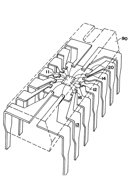
In one embodiment of the present invention, as shown in Figure
2, there is provided a plastic encapsulated~package~ comprising a
chip 11 having die pads 12 which is mounted upon a diamond
substrate 20. Leads or legs 13 having leg connection bonding pads
14 are not only placed in electrical connection with chip 11 via
wires 16, they are also placed in intimate thermal contact with
diamond fil~ 20 by virtue of their abutment thereto. The entire
pac~age is encapsulated in plastic molding 90, save one end of each
leg. Because diamond film is an excellent electrical insulator, its
presence does not effect the transmission of information between
chip 11 and legs 13. Because diamond film is also an excellent
th~rm~l conductor, heat generated within chip 11 flows through the
2152132
diamond film and into each of the eight legs 13 and subsequently
out of the package ~ . In contrast to the prior art design shown
in Figure 1, wherein heat generated by the chip is dissipated
directly (and poorly) only through thin wires and through the
plastic molding, the present invention allows heat from the
substrate to be dissipated not only-through the thin wires and
plastic molding but also directly through each of the wide leads
13. Because the present invention presents many more avenues for
heat dissipation than the conventional design, it will dissipate
heat much faster. Thermal analysis of the legs and encap~ulant
reveals that the copper leads have a thermal conductivity of about
228 BTU/(hr ft F) while the polyamide has a thermal conductivity of
only about 0.19 BTU/(hr ft F~. Since the thermal conductivity of
the legs are about 1000 times superior to that of the encapsulant,
lS it is contemplated that the advantage o~ the present invention
increases essentially directly with the number of legs in the
pac~age.
In one embodiment of the present invention containing 24 legs,
finite element analysis revealed that the Tja (i.e., the
temperature differential between the device junctlon and the
ambient temperature) was only about 60 degrees C. In contrast, the
Tja for a comparable conventional IC pac~age was about 400 C for
the same power input.
~ 2l52l32
The method by which the diamond film is attached to the chip
can be any conventional attachment means, including soldering,
clamping, bonding agents, and silver loaded epoxies. Similarly, the
method by which the diamond film is attached to the~legs of the
package can be any conventional attachment means, including
clamping, soldering, bonding agents,- silver loaded epoxies, and
brazing.
Any conventional chip and lead frame design can be used with
the present invention as long as the design allows for a diamond
film to be in intimate thermal contact with both the chip and the
legs of the lead frame. Conventional chips include integrated
circuits and discrete active devices such as transistors and
diodes. Conventional pac~age designs include both plastic and
ceramic DIP, SIP, PGA, QFP, BGA and LCC designs. When another
thermally conductive, elec~rically resistive substrate other than
diamond is used for a die pad, the IC package of the present
invention is plastic encapsulated.
Because the thermally conductive, electrically resistive base
o~ the present invention provides for greater heat dissipation, the
IC packages of the present invention can tolerate larger amounts of
power than the standard package without exceeding the critical
device junction temperature. In particular, the present invention
provides an improved JEDEC pac~age capable of dissipating up to at
least about 600~ more power than the st~n~rd JEDEC package in
.
~ 21~2132
forced air with a convection coefficient of about 50 W/m2 C at 50 C
while still maint~;n;ng a maximum junction temperature of 125 C.
In one embodiment, finite element analysis revealed that a 24 pin
DIP of the present invention was capable of dissipating about 12
watts of power in forced air with a convection coefficient of about
50 W/m2 C at 50 C while- still maintaining a maximum junction
temperature of 125 C. In contrast, the standard JEDEC 24 pin DIP
could dissipate only 1.6 watts.
'~!,
. -,. . .