Note: Descriptions are shown in the official language in which they were submitted.
WO94/153~2 ~1 5 2 ~ 7 ~ PCT~S93/11791
TRIODE STRUCTURE FLAT PANEL DISPLAY EMPLOYING FLAT
FIELD EMISSION CATHODES
RELATED APPLICATION
This application is a continuation-in-part of
Serial No. 07/851,701, which was filed on March 16,
1992, is entitled "Flat Panel Display Based on Diamond
Thin Films" and is incorporated herein by reference.
TECHNICAL FIELD OF THE INVENTION
This invention relates, in general, to flat panel
displays for computers and the like, and, more
specifically, to flat panel displays that are of a
field emission type using a tr`iode (three terminal)
pixel structure with flat cathode emitters in which the
pixels are individually addressable.
W094/15352 ~l~i2~'12 -2- PCT/[JS93/1179
BACKGROUND OF THE INVENT I ON
Field emission computer displays, in the general
sense, are not new. For years there have been displays
which comprise a plurality of field emission cathodes
and corresponding anodes, the anodes emitting light in
response to electron bombardment from corresponding the
cathodes. Before entering a discussion on such
displays, however, it is helpful to gain an
understanding of the nature of field emission.
Field emission is a phenomenon which occurs when
an electric field proximate the surface of an emission
material narrows the width of a potential barrier
existing at the surface of the emission material. This
allows a quantum tunnelling effect to occur, whereby
electrons cross through the potential barrier and are
emitted from the material.
The field strength required to initiate emission
of electrons from the surface of a particular material
depends upon that material's "work function." Many
materials have a positive work function and thus
require a relatively intense electric field to bring
about field emission. Some materials do, in fact, have
a low, or even negative, work function and thus do not
require intense fields for emission to occur. Such
materials may be deposited as a thin film onto a
conductor, resulting in a cathode with a relatively low
threshold voltage required to produce electron
emiss ions .
In prior art devices, it was desirable to enhance
field emission of electrons by providing for a cathode
geometry which focussed electron emission at a single,
relatively sharp point at a tip of a conical cathode
(called a micro-tip cathode). These micro-tip
21~2~2
WO94/15352 PCT~S93111791
--3--
cathodes, in conjunction with extraction grids
proximate the cathodes, have been in use for years in
triode field emission displays.
For example, U.S. Patent No. 4,857,799, which
issued on August 15, 1989, to Spindt et al., is
directed to a matrix-addressed flat panel display using
field emission cathodes. The cathodes are incorporated
into the display backing structure, and energize
corresponding cathodoluminescent areas on a face plate.
The face plate is spaced 40 microns from the cathode
arrangement in the preferred embodiment, and a vacuum
is provided in the space between the plate and
cathodes. Spacers in the form of legs interspersed
among the pixels maintain the spacing, and electrical
connections for the bases of the cathodes are diffused
sections through the backing structure. Spindt et al.
employ a plurality of micro-tip field emission cathodes
in a matrix arrangement, the tips of the cathodes
aligned with apertures in an extraction grid over the
cathodes. With the addition of an anode over the
extraction grid, the display described in Spindt et al.
is a triode display.
Unfortunately, micro-tips employ a structure which
is difficult to manufacture, since the micro-tips have
fine geometries. Unless the micro-tips have a
consistent geometry throughout the display, variations
in emission from tip to tip will occur, resulting in
unevenness in illumination of the display.
Furthermore, since manufacturing tolerances are
relatively tight, such micro-tip displays are expensive
to make.
Another example of micro-tip cathodes is found in
U.S. Patent No. 5,038,070, which issued on August 6,
1991 to Bardai et al., directed to a triode display and
-
WO 94/15352 PCTIUS93/11791
2~ 2
discloses a plurality of field emitters in the form of
hollow, upstanding pointed cones or pyramids formed by
a molding process. The plurality of field emitters
extend from a surface of an electrically conductive
layer. An electrically conductive mesh is adhered to
an opposite surface of the conductive layer by a high
temperature brazing process in electrical connection
with the conductive layer. The mesh provides a strong
metal base with good thermal conductivity for mounting.
Additional elements such as a gate and anode structure
may be formed on the conductive layer in alignment with
the field emitters to form a field emitting triode
array or the like.
A disadvantage of the field emitter structure
taught in Bardai et al. is that emitter cones must be
photolithographically grown, which is a very complex
and expensive procedure.
Yet another triode micro-tip structure is
illustrated in "Recent Developments on 'Microtips'
Display at LETI," published in the Technical Digest of
IVMC, Nagahama, 1991. Author R. Meyer describes a
micro-tip display having two salient features: (1) cold
electron emission by field effect from a large matrix
array of "micro-guns" (or micro-tips) and (2) low-
voltage cathodoluminescence (of a few hundred volts).Again, Meyer uses micro-tip cathodes which have the
disadvantages which have been noted above.
Another patent to Spindt et al., U.S. Patent
No. 5,015,912, which issued on May 14, 1991, teaches a
matrix-addressed flat panel display using micro-tip
cathodes of the field emission type. Spindt et al.
discloses a grid structure for use in conjunction with
micro-tip cathodes.
2152472
WO94/1~352 PCT~S93/11791
--5--
An attribute of the invention disclosed in Spindt
et al. is that it provides its matrix-addressing scheme
entirely within the cathode assembly. Each cathode
includes a multitude of spaced-apart electron emitting
tips which project upwardly therefrom toward a face
structure. An electrically conductive gate or
extraction electrode arrangement is positioned adjacent
the tips to generate and control electron emission from
the latter. Such arrangement is perpendicular to the
base stripes and includes apertures through which
electrons emitted by the tips may pass. The extraction
electrode is addressed in conjunction with selected
individual cathodes to produce emission from the
selected individual cathodes. The grid-cathode
arrangement is necessary in micro-tip cathodes
constructed of tungsten, molybdenum or silicon, because
the extraction field necessary to cause emission of
electrons exceeds 50 MV/m. Thus, the grid must be
placed close (within approximately l micrometer) to the
micro-tip cathodes. These tight tolerances require
that the gate electrodes be produced by optical
lithographic techniques on an electrical insulating
layer which electrically separates the gates of each
pixel from the common base. Such photolithography is
expensive and difficult to accomplish with the accuracy
required to produce such a display, thereby raising
rejection rates for completed displays. Moreover, the
extraction grid taught in Spindt et al. was
specifically designed to operate in conjunction with
micro-tip cathodes, and not with other geometries.
The two major problems with the device disclosed
in Spindt et al. are l) formation of the micro-tip
cathodes and 2) formation and alignment of the
extraction electrodes with respect to the cathodes.
The structure disclosed in Spindt et al. is extremely
WO94/15352 PCT~S93/11791
2~2~72 -6-
intricate and difficult to fabricate in the case of
large area displays.
The prior art has been directed to micro-tip
cathodes, even in view of their formidable
manufacturing difficulties, because they are
advantageously used with an extraction grid in a triode
(three terminal) structure.
In a triode (three terminal) pixel structure, an
electron extraction grid structure is interspersed
between corresponding cathode and anode pairs. In the
case of triode displays, the grid gives an extra
control parameter which produces several advantages.
First, the grid can be controlled independent of the
cathodes and anodes to thereby produce independently
controllable cathode-anode and cathode-grid electric
fields. This allows use of a very low control voltage
to be applied to the cathode-grid field to effect
electron emission, while the grid-anode voltage can be
very high (several hundred to several thousand volts)
to thereby result in higher power efficiency of the
display. This is so because the anode phosphor
material can be excited by electrons falling through a
greater potential and, hence, be struck by electrons
having a greater kinetic energy. Second,.voltages
selectively applied to address and excite individual
grid-anode pairs can be lower (on the order of 40
volts), thereby allowing use of more conventional
electronics in drive circuitry. Finally, the lower
electric field between the grid and the anode (on the
order of 1-5 volts per micrometer) reduces dielectric
requirements for spacer material used to separate
cathode and anode assemblies. Prior art extraction grid
structures were designed to cooperate with micro-tip
21~ 2 4 7 2 PCT~S93/11791
WO94115352
--7--
cathodes to enhance control of electron extraction and
emission.
In Serial No. 07/851,701, which was filed on March
16, 1992, and entitled "Flat Panel Display Based on
Diamond Thin Films," an alternative cathode structure
was first disclosed. Serial No 07/851,701 discloses a
cathode having a relatively flat emission surface. The
cathode, in its preferred embodiment, employs an
emission material having a relatively low effective
work function. The material is deposited over a
conductive layer and forms a plurality of emission
sites, each of which can f~ield-emit electrons in the
presence of a relatively low intensity electric field.
Flat cathodes are much less expensive and
difficult to produce in quantity because the fine,
micro-tip geometry has been eliminated. The advantages
of the flat cathode structure was discussed at length
therein. The entirety of that application, which is
commonly assigned with the present invention, is
incorporated herein by reference.
A relatively recent development in the field of
materials science has been the discovery of amorphic
diamond. The structure and characteristics of amorphic
diamond are discussed at length in "Thin-Film Diamond,"
published in the Texas Journal of Science, vol. 41, no.
4, 1989, by C. Collins et al., the entirety of which is
incorporated herein by reference. Collins et al.
describe a method of producing amorphic diamond film by
a laser deposition technique. As described therein,
amorphic diamond comprises a plurality of
micro-crystallites, each of which has a particular
structure dependent upon the method of preparation of
the film. The manner in which these micro-crystallites
-
WO94/15352 PCT~S93/11791
21~247 2 -8-
are formed and their particular properties are not
entirely understood.
Diamond has a negative electron affinity in the
(lll) direction. Thus n-type diamond has a negative
work function. That is, only a relatively low electric
field is required to distort the potential barrier
present at the surface of diamond. Thus, diamond is a
very desirable material for use in conjunction with
field emission cathodes. In fact, the prior art has
employed diamond films to advantage as an emission
surface on micro-tip cathodes. However, the prior art
has failed to recognize that amorphic diamond, which
has physical qualities which differ substantially from
other forms of diamond, makes a particularly good
emission material. Serial no. 07/851,701 was the first
to disclose use of amorphic diamond film as an emission
material. In fact, in the preferred embodiment of the
invention described therein, amorphic diamond film was
used in conjunction with a flat cathode structure to
result in a radically different field emission cathode
design. The micro-crystallites present in the amorphic
diamond film are more or less disposed to function as
electron emission sites, depending upon their
individual structure. Therefore, over the surface of a
relatively flat cathode emission surface, amorphic
diamond micro-crystallites will be distributed about
the surface, a percentage of which will act as
localized electron emission sites.
The prior art has been entirely directed to triode
flat panel displays based on micro-tip cathodes
constructed of molybdenum, tungsten, silicon or similar
materials. The prior art has failed to provide a
matrix-addressable flat panel display that is 1)
relatively simple in design, 2) relatively inexpensive
~ W094/15352 21 S 2 4 7 2 PCT~S93/11791
to manufacture and 3) uses a triode (three terminal)
pixel structure employing a cathode which has a
relatively flat emission surface comprising a plurality
of distributed localized electron emission sites.
The prior art has also failed to address the
problem of providing an appropriate grid structure for
use in conjunction with flat cathodes.
The purpose of the present invention is to build
on the idea of depositing amorphic diamond film on the
surface of relatively flat field emission cathodes, by
providing a triode display structure employing a novel
extraction grid proximate ~he flat cathodes to cause
emission therefrom.
WO94/15352 PCT~S93/11791 ~
2~ 52 ~7 ~ -lo-
SUMMARY OF THE INVENTION
The present invention relates to a flat panel
display arrangement which employs the advantages of a
luminescent phosphor of the type used in CRTs, while
maintaining a physically thin profile. Specifically,
the present invention provides for a flat panel display
comprising (l) a plurality of corresponding light-
emitting anodes and field-emission cathodes, each of
the anodes emitting light in response to emission from
each of the corresponding cathodes, each of the
cathodes including a layer of low work function
material having a relatively flat emission surface
comprising a plurality of distributed localized
electron emission sites and (2) a grid assembly
interspersed between the corresponding anodes and
cathodes to thereby control emission levels to the
anodes from the corresponding cathodes, the grid
assembly having apertures therein, the apertures having
diameters equal to that of corresponding cathodes, such
that the cathodes do not lie under the grid assembly.
In other words, the flat panel display is of a
field emission type using a triode (three terminal)
pixel structure. The display is matrix-addressable by
using grid and cathode assemblies arranged in strips in
a perpendicular relationship whereby each grid strip
and each cathode strip are individually addressable by
grid and cathode voltage drivers, respectively.
Effectively, a "pixel" is formed at each intersection
of a grid strip and a cathode strip. The result is
that each pixel within the display may be individually
illuminated.
The grid strips themselves have a novel construction
which allows them to operate with flat cathodes. More
specifically, the grid strips comprise a substrate,
~ WO94/15352 21~ 2 ~ 72 PCT~S93/11791
--11--
preferably of SiO2, upon which is deposited a
conductive layer, preferably of a metal. The
conductive layer is etched to produce apertures
therein, the apertures corresponding to particular
cathode-anode pairs, edges of the apertures being
located substantially above edges of corresponding
cathodes.
The cathode assembly comprises a plurality of flat
cathodes are, in the preferred embodiment of the
present invention, photolithographically patterned
either (1) through the apertures in the grid or (2) in
alignment with the apertures in the grid. Each cathode
comprises a conductive material deposited over a
substrate and a resistive material deposited over the
conductive material. A thin film of low effective work
function is then deposited over the resistive layer.
The resistive layer provides a degree of electrical
isolation between various subdivisions of the cathode
strips.
The anode assembly consists of a conductive
material (such as indium-tin oxide in the preferred
embodiment) deposited over a substrate with a low
energy phosphor (such as zinc oxide in the preferred
embodiment), deposited over the conductive layer. In
an alternative embodiment of the present invention, a
plurality of red, green and blue phosphors can be
deposited over the conductive layer to provide a color
display.
The resulting anode assembly and cathode
assemblies are joined together with a peripheral glass
frit seal onto a printed circuit board. Proper spacing
between the assemblies is maintained by spacers
consisting of either glass fibers or glass balls or a
fixed spacer produced by typical deposition technology.
WO94/15352 PCT~S93/11791 ~
2152~7~ -12-
The assemblies are hermetically sealed and a vacuum
drawn within the space between the anode and cathode
assemblies via an exhaust tube. Systems for
maintaining vacuums within such structures are well
known in the art. Residual gases within the vacuum are
collected together by a device called a getter.
The individual rows and columns of grid strips and
cathode strips are externally accessible by flexible
connectors provided by typical semiconductor mounting
technology. These connectors are attached to grid and
cathode drivers so as to provide the addressability of
each pixel within the display.
An individual pixel is illuminated when the
electrical potential difference between portions of a
cathode and grid strip corresponding to that pixel is
sufficient to extract electrons from the emission
material coating the cathode, thereby causing emission
of electrons from the cathode, through the control grid
and toward the anode. As the electrons travel to the
anode, they strike the low energy phosphor material,
thereby producing light.
In a triode display, the gap between the cathode
and grid is on the order of l micrometer. Because the
spacing is so close, only 40 volts or so is required to
cause emission. Commercially available devices are
available in the prior art to switch 40 volts. These
voltage drivers are also referred to as grid drivers
and cathode drivers. A pixel is addressed and
illuminated when the required driver voltage is applied
to a corresponding grid strip and cathode strip
resulting in emission of electrons from that portion of
the cathode strip adjacent to the grid strip.
Electrons are not emitted in a particular pixel area if
only the corresponding cathode strip or corresponding
WO94/15352 ~ I 52 ~ 72 PCT~S93/11791
-13-
grid strip is driven by the required driver voltage
since the required threshold potential between the
cathode and grid is not achieved.
- The present invention has the ability to implement
the display in grey scale mode by controlling the
voltage supplied to the control grid which, in turn,
modulates emissions of electrons from the cathode to
the anode, thus varying photon emission of the phosphor
material deposited on the anode.
The grid is supported by a layer of dielectric
material. The dielectric material is anisotropically
etched to eliminate dielectric material between the
cathode and its corresponding aperture. This results
in the existence of a plurality of mushroom-shaped
structures of dielectric material supporting the grid
layer. In the alternative the dielectric layer can be
isotropically etched until the mushroom-shaped
structures are etched away, leaving the grid locally
suspended. This results in an air-bridge structure.
Some of the advantages of the present invention
include low power consumption, high brightness and low
cost. Additionally, the cathode assembly of the present
invention is less complicated and less expensive to
manufacture since sophisticated photolithography is not
required to produce the preferred flat cathode
arrangement and grid assembly.
The foregoing has outlined rather broadly the
features and technical advantages of the present
invention in order that the detailed description of the
invention that follows may be better understood.
Additional features and advantages of the invention
will be described hereinafter which form the subject of
the claims of the invention. It should be appreciated
~ 1~ 2 ~ 7 2 - l4- PCT~S93/11791
by those skilled in the art that the conception and the
specific embodiment disclosed may be readily used as a
basis for modifying or designing other structures for
carrying out the same purposes of the present
invention. It should also be realized by those skilled
in the art that such equivalent constructions do not
depart from the spirit and scope of the invention as
set forth in the appended claims.
WO94/15352 215 2 4 ~ 2 ~CT~S93/11791
-15-
BRIEF DESCRIPTION OF THE DRAWINGS
For a more complete understanding of the present
invention, and the advantages thereof, reference is now
- made to the following descriptions taken in conjunction
with the accompanying drawings, in which:
FIGURE 1 illustrates a top view of joined cathode
and extraction grid assemblies;
FIGURE 2 illustrates a cross-sectional side view
of a triode display;
FIGURE 3 illustrates a partial side view of the
joined cathode and extraction grid assemblies of
FIGURE 2;
FIGURE 4 illustrates a partial side view of an
emitter array without supporting pillars before cathode
deposition;
FIGURE 5 illustrates a partial side view of an
emitter array without supporting pillars after cathode
deposition;
FIGURE 6 illustrates a partial side view of an
emitter array with supporting pillars before cathode
deposition;
FIGURE 7 illustrates a partial side view of an
emitter array with supporting pillars before cathode
deposition;
FIGURE 8 illustrates an ineffective-grid
structure; and
FIGURE 9 illustrates a perspective view of the
joined cathode and extraction grid assemblies with an
intervening dielectric layer.
, . . . _ = .
....
WO94/153~2 2 ~ 5 2 4 7 2 PCT~S93111791
-16-
DETAILED DESCRIPTION OF THE rNvENTIoN
Turning now to FIGURE l, shown is a top view of
joined cathode and extraction grid assemblies of the
present invention. Their structure and function will
be more completely described in a description
pertaining to FIGURE 2. The grid structure 102 is
divided into electrically isolated and individually
addressable strips which are arranged in a
perpendicular manner with cathode strips, which,
together, form a cathode structure l0l. The cathode
strips are parallel to anode strips (not shown). In
this orthogonal arrangement, the strips in the
structures l0l, 102 provide a vertically and
horizontally addressable structure which forms the
basis for a flat panel display. External connectors
220 provide electrical access to the cathode structure
l0l and the grid structure 102. In the preferred
embodiment of the present invention, the cathode strips
and grid strips are separated by a dielectric layer.
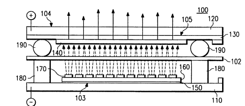
Turning now to FIGURE 2, shown is a side view of a
"pixel" l00 of a triode flat panel display of the
present invention. Each cathode strip 103 of the
cathode structure l0l of FIGURE l comprises a substrate
l0l, a conductive layer 150, a resistive layer 160 and
flat cathodes 170. The individual flat cathodes 170
are spaced apart from each other resulting in their
isolation maintained by the resistive layer 160. The
anode assembly 104 consists of a substrate 120,
typically glass, a conductive layer 130, typically
indium-tin oxide (ITO) and a low energy phosphor 140,
such as zinc oxide (ZnO). However, if a color display
is desired, then red, green and blue phosphors can be
substituted for the ZnO. The anode assembly 104 is
separated from a grid structure 102 by a plurality of
21~2472
WO94/153~2 PCT~S93/11791
-17-
dielectric spacers l90, which maintain a desired
distance of separation between the anode assembly 104
and the grid structure lO2.
Interspersed between the cathode strips 103 and
anode assembly 104 is the grid structure 102.
Electrons passing through openings in the grid
structure 102 are accelerated toward the conductive
layer 130, striking the low energy phosphor 140 and
causing the low energy phosphor to emit light in
response thereto. The grid structure 102 is separated
from a substrate under the cathode strips 103 by a
spacer 180 which, in the preferred embodiment of the
present invention, is a layer of dielectric material,
preferably silicon dioxide (sio2). As will be
lS explained later, apertures will be etched through the
grid structure and the SiO2 to form a channel from the
cathodes, through corresponding apertures in the grid
structure and to the corresponding anodes.
The pixel lO0 is illuminated when a sufficient
driver voltage is applied between the conductive layer
150 associated with the pixel lO0 and the grid
structure 102 corresponding to that particular pixel
lO0. The two driver voltages combine with the constant
DC supply voltage to provide a sufficient threshold
potential between the sections of the grid and cathode
structures 102, lOl (both of FIGURE 1) associated with
the pixel lO0. The threshold potential results in
electron emission from the flat cathodes 170.
Turning now to FIGURE 3, shown is a partial side
view of the joined cathode and extraction grid
assemblies of FIGURE 2, taken along Section 3-3 of
FIGURE 2. In the embodiment shown in FIGURE 3, spacers
180 are provided to maintain the proper distance
between the grid structure 102 and the substrate under
WO94/15352 ~5 2 ~7 2 PCT~S93/11791
-18-
the cathode strips 103. Again, the spacers 300 are
preferably a layer of dielectric material. The grid
structure 102 is provided with a plurality of apertures
310 therein, the apertures aligned or to be aligned
with corresponding cathodes (not shown~.
Turning now to FIGURE 4, shown ~is a partial side
view of an emitter array without supporting pillars
before cathode deposition. The emitter array comprises
the substrate, cathode conductive layer and resistive
layer, all illustrated and described in detail with
respect to FIGURE 1. An SiO2 dielectric layer 400 is
deposited over the substrate and provides a base for an
extraction gate conductive layer 102. As shown in
FIGURE 4, layer 102 has already been deposited on layer
400 and apertures photolithographically etched therein.
Since FIGURE 4 is a cross-section, the apertures are
shown as spaces in the layer 102. Once the apertures
have been etched, the SiO2 layer is isotropically
etched until it is removed from under that part of the
layer 102 which is between the dielectric layer 400.
Because a plurality of gate apertures corresponding to
a particular pixel are closely spaced in the region of
the pixel, isotropic etching of the SiO2 layer results
in an air-bridge structure wherein the layer 102 is
locally suspended over the pixel, without support from
pillars therein. Even though a particular pixel
comprises a plurality of cathodes and gate apertures in
the preferred embodiment of the present invention, the
layer 102 is still supported on all sides around the
pixel by the layer 400, as shown in FIGURE 4. Note in
particular, however, that the isotropic etch of the
SiO2 results in the layer 102 being etched back
somewhat from the edges of the various apertures. This
is an important feature of the present invention and
will be explained in detail with respect to FIGURE 5.
~ W094/15352 215 2 ~ 72 PCT~S93111791
--19--
Turning now to FIGURE 5, shown is a partial side
view of an emitter array without supporting pillars
after cathode deposition. Cathodes 500 are shown as
having been deposited through the apertures and on the
~ 5 resistive layer. It is important to note that the
cathodes are as wide as the apertures in the grid
structure. It is a key feature of the present
invention that the cathodes lie entirely under the
apertures. This is so that the electric field existing
about a cathode by virtue of the grid is relatively
uniform over the surface of the cathode. This results
in even electron emission over the surface.
Furthermore, since no part of the cathodes lie directly
under the grid, electrons, once emitted, do not have a
tendency to strike the grid instead of the anode. This
results in greater display efficiency, because power is
not wasted on electrons which will fail to strike the
anode.
Turning now to FIGURE 6, shown is a partial side
view of an emitter array with supporting pillars before
cathode deposition. Once apertures are etched in the
grid layer 102, the SiO2 dielectric layer 400
underneath is anisotropically etched until all SiO2 is
etched away from under the apertures. This leaves a
plurality of mushroom-shaped pillars 600 between the
individual apertures.
Turning now to FIGURE 7, shown is a partial side
view of an emitter array with supporting pillars before
cathode deposition. It is important to note that the
cathodes are as wide as the apertures in the grid
layer. It is also important to note that the pillars
600 are etched somewhat back from the edges of the
apertures in the grid layer. Recall, as in the case of
FIGURE 5, that the cathodes to be deposited are of the
WO94/15352 ~5 2 4 ~ 2 PCT~S93111791
-20-
same diameter as the apertures. It is highly
undesirable to allow the dielectric layer to touch the
cathodes directly (thereby creating a "triple junction"
of cathode, SiO2 and space), otherwise electrons
emitted from the cathodes have a tendency to climb the
walls of the dielectric layer, creating a low
resistance path and inhibiting emission of electrons to
the corresponding anode. This, as in the case described
above, results in display inefficiency. Therefore, by
providing a dielectric layer etched back from the
apertures and thus removed by a small distance from the
cathode, this phenomenon is minimized.
The method of depositing the cathodes through the
apertures in the grid conductive layer, using the grid
conductive layer as a mask, is the preferred manner of
producing the present invention. In an alternative
method to that illustrated in FIGURES 4-7, the cathodes
can be formed over the cathode conductive layer prior
to deposition of the dielectric layer and the grid
conductive layer, instead of depositing the cathodes
through apertures in the grid conductive layer. One
disadvantage of this alternative method, however, is
that careful attention must be paid to alignment of the
cathodes with respect to the apertures in the grid
conductive layer. Should misalignment occur, display
inefficiency or inoperability might result.
Turning now to FIGURE 8, shown is an ineffective
grid structure. The structure, generally designated
801, comprises a cathode substrate 802, upon which is
deposited a cathode conductive layer 803 and strips of
a cathode emission material layer 804. A dielectric
layer 80~ is deposited on the material layer 804 to
form strips which are oriented so as to be
perpendicular to the strips of cathode emission
~ WO94/15352 21 5 2 ~ 7 2 PCT~S93/11791
material and etched to form apertures which define
individual cathode-anode pairs. A grid layer 806 of
~ conductive material is next deposited on the dielectric
layer 805, the grid layer 806 formed in strips
~ 5 corresponding to those of the dielectric layer 805 and
having corresponding apertures therein. An anode
assembly 807 comprising a phosphor layer is placed
above the grid layer 806 and held a controlled distance
from the grid layer by a plurality of fibrous
dielectric spacers 808.
Although the structure 801 is compatible with flat
cathodes, it has several disadvantages. First, the
electric field under the grid layer 806 is much higher
than the field existing between the grid layer 806
strips. As previously mentioned, this results in many
of the emitter electrons being directed, not to the
anode 807, but to the grid layer 806. Since these
electrons never strike a phosphor, the energy in them
is wasted.
Second, the ratio of the electric field at and in
the apertures in the grid layer 806 strips depends upon
the diameter of the grid layer 806 apertures and the
thickness of the dielectric layer 805. For good
display operation, the diameter of the apertures and
the thickness of the dielectric layer 805 should have,
at most, a one-to-one correspondence. In the preferred
embodiment of the present invention, the size of the
apertures is approximately l to 20 micrometers in
diameter.
Third, the fact that the emission layer 804
extends fully across the aperture gives rise to excess
emission from the parts of the emission layer proximate
the dielectric material (at the "triple junction"). In
other words, emission from the emission layer 804 is
=
WO94/15352 PCT~S93111791
-22-
not uniform from one side to another. It is much
stronger on the edges of the cathode. This gives rise
to leakage currents along the surface of the dielectric
layer 805, causing the emission layer 804 and the grid
layer 806 to short across the dielectric layer 805,
thereby hampering or totally disabling operation of the
pixel. Thus, the structure 801~`is deficient.
The key difference between the structure of
FIGURE 8 and those preferred structures shown in
FIGURES 5 and 7 is that the emission layer 804 is a
uniform layer having triple junctions, whereas
individual cathodes are shown in FIGURES 5 and 7, the
cathodes having been deposited through the gate
apertures or previously deposited in alignment with the
apertures. In either case, the cathodes reside
directly underneath the apertures and do not extend to
under the gate conductors, which has been previously
described as disadvantageous and is evident in
FIGURE 8.
Furthermore, in the case of FIGURE 7, wherein
mushroom-shaped SiO2 dielectric supports exist between
the individual cathodes, the dielectric supports are
separated from the cathodes so as to eliminate triple
junctions and thereby reduce the occurrence of surface
current leakage. These emitters do not extend from one
side to another of the aperture formed into the grid
layer and thus do not come into contact with the
dielectric layer, thereby minimizing the occurrence of
leakage currents. Instead the cathodes are discrete
units, deposited separately upon the conductive layer.
Turning now to FIGURE 9, shown is a perspective
view of the joined cathode and extraction grid
assemblies with an intervening dielectric layer. Shown
is a substrate 90l upon which is deposited a conductive
WO94/15352 21 52~ 7~ PCT~S93/11791
-23-
layer 902, as described before. The conductive layer
902 is deposited in strips, as shown. A dielectric
layer 903 is deposited in a blanket layer over the
conductive layer 902 and portions of the substrate 901.
Next, a control grid layer 904 is deposited on the
dielectric layer 903 in the form of strips oriented
perpendicularly with respect to the conductive layer
902 strips and provided with a plurality of apertures
corresponding to those in the dielectric layer 903. A
plurality of apertures 906 are formed in the dielectric
layer 903 which correspond to cathodes created or to be
created in the conductive layer 902. The grid layer
904 terminates in a plurality of end conductors 905
which can be coupled to drive circuitry allowing the
grid layer 904 to be selectively potentially separated
from the conductive layer 902. For purposes of FIGURE
9, the anode layer and fibrous spacing material have
not been shown although, if shown, would reside over
the grid layer 904.
From the above description, it is apparent that
the present invention is the first to provide a flat
panel display comprising (l) a plurality of
corresponding light-emitting anodes and field-emission
cathodes, each of the anodes emitting light in response
to emission from each of the corresponding cathodes,
each of the cathodes including a layer of low work
function material having a relatively flat emission
surface comprising a plurality of distributed localized
electron emission sites and (2) a grid assembly
interspersed between the corresponding anodes and
cathodes to thereby control emission levels to the
anodes from the corresponding cathodes.
Although the present invention and its advantages
have been described in detail, it should be understood
-
WO 94/15352 ~ 2 iS ~ 4~ PCT/US93/11791 ~
-24-
that various changes, substitutions and alterations can
be made herein without departing from the spirit and
scope of the invention as defined by the appended
claims.