Note: Descriptions are shown in the official language in which they were submitted.
H5979,SE987 215 2 6 5 9
MULTISTANDARD DECODER FOR VIDEO SIGNALS AND VIDEO SIGNAL
DECODING METHOD
The invention relates to a digital multistandard decoder for video signals and to a method
for decoding video signals.
Color video signals, so-called composite video, blanking and sync signals (CVBS;) are
essentially composed of a brightness signal or luminance component (Y), two color difference
5 signals or chrominance components (U, V or I, Q), vertical and horizontal sync signals (VS, HS)
and a blanking signal (BL). The structure off a composite video signal (CVBS) and the
corresponding Y, U and V signals is shown in Fig. 1.
Fig. 1 a shows a composite video signal for an EBU (European Broadcasting Union) color
bar test signal, in which on the lllmin~nce component Y are additively superimposed the six hue
10 (tint) values belonging to the vertical color bar in "carrier packets" with color carrier frequency.
For the color carrier generation a color subcarrier frequency sync signal, the burst, is transmitted
directly behind the line sync pulse, SYNC. The burst phase and the burst amplitude are used as
reference values for determining the hue and the color saturation of the demodulated signal,
which is represented by the individual carrier packets.
The different coding processes, e.g. NTSC, PAL and SECAM, introduced into the known
color television standards, differ in the nature off the chrominance transmission and in particular
the different systems make use of different color subcarrier frequencies and different line
frequencies.
The following explanations relate to the PAL and NTSC systems, but correspondingly
20 apply to video signals of other standards and non-standardized signals.
The color subcarrier frequency (fsc) of a PAL system and a NTSC system is
fsc(NTSC) = 3.58 MHz or
fsc(PAL) = 4.43 MHz.
In addition, in PAL and NTSC systems the relationships of the color subcarrier frequency
25 (fsc) to the line frequency (fh) are given by
fsc(NTSC) = 227.50 * fh or 4-fsc (NTSC) = 910 fh
fsc(PAL) = 283.75 * fh or 4--fsc (PAL) = 1135 fh
~ H5979,SE987 21 S 2 6 5 9
so that the phase of the color subcarrier in the case of NTSC is changed by 1 80/line and in PAL
by 270/line.
In the case of digital video signal processing and decoding the prior art fundamentally
distinguishes between two system architectures. These are the burst-locked architecture and the
5 line-locked architecture, i.e. systems which operate with sampling frequencies for the video
signal, which are produced in phase-locked manner to the color subcarrier frequency transmitted
with the burst pulse or in phase-locked manner with the line frequency, respectively.
In the case of decoders with a burst-locked architecture the sampling frequency is chosen
in such a way that on the one hand it is not too high so as to keep the power loss low and on the
10 other hand so that the Nyquist theorem is fulfilled. i.e. fa >2--fsc. For problem free processing
of the modulated color carrier in the decoder it is ~propl;ate to use a sampling frequency which
corresponds to the even multiple of the color subcarrier. Four times the color subcarrier
frequency is best suited for this.
In the case of line-locked architectures the clock of the digital system is derived from the
15 line frequency and is an integer multiple of the line frequency, so that an integer number of pixels
per line are produced.
Although the burst-locked system has advantages with respect to the minimum effort and
expenditure for color decoding, from other standpoints it also has important disadvantages, e.g.
in the case of horizontal and vertical synchronization. as well as in multistandard and
20 "non-standard" uses. AS the sampling process is essentially non-orthogonal, the burst- locked
system is only suitable for the direct representation of images on a screen, but not for producing
data for fixed raster applications. e.g. for field or frame stores or for frame grabbers in a PC
environment.
However, although the line-locked systems solve the problems of burst-locked
25 architectures in a satisfactory manner, they still lead to new problems. In particular, much more
complex color decoders are required, the analog clock generation requires a high circuitry
expenditure and the requirements for the maximum acceptable dynamic non-linearities ofthe A/D
converters and preceding analog signal processing stages are very high.
Both systems suffer from the disadvantages that the clock frequencies for digitizing the
30 video signal are derived from the video system, namely from the color subcarrier frequency or
H5979,SE987 21 S 2 6 ~ 9
from the line frequency, whereas e.g. in a PC environment working takes place with completely
different clock frequencies, so that due to the different clock frequencies in the overall system
intermodulation products and crosstalk of signals can have a disturbing effect on the overall
operation -and the image quality. As the clock frequencies of PC's are not generally suitable for
5 sampling video signals, because they do not satisfy the above-explained conditions, the prior art
decoders in each case have their own oscillators for producing the sampling frequency suitable
for a particular television standard.
In summarizing, Table I gives dir~ sampling frequencies and their
advantages/disadvantages for digital video processing:
TABLE I
Sampling Frequency Advantages Disadvantages
Burst-locked (4--f s c) Simple color decoder. No Complicated line
distortion due to synchronization. A sample
non-linearities. rate conversion is necessary
for field/frame storages. For
multistandard operation
multiple crystals are
necessary.
Simple field/frame storage.
Line-locked (n-fH) Only one crystal for Complicated color decoder.
multistandard operation. Sensitive to non-linearities in
composite video signal.
The best choice with respect to these factors is dependent on the sought market. the
15 function and intended use of the decoder. A rough survey is given in Table II.
TABLE II
Market Use Preferred Sampling
TV set Replacement of analog Burst-locked
clrcuit.
TV set Additional features Line-locked
(field/frame store)
20 Desk top video (PC) Fixed video image size in a Burst-locked
window.
Desk top video (PC) Scalable video image size in Line-locked
a window.
The problem of the invention solves the above problems by providing a decoder for
digital video signals and a composite video signal decoding method, which can process video
H5979,SE987 2152659
signals according to di~el~lll standards on the basis of a random, predetermined clock frequency
of a host system, e.g. a PC.
This problem is solved by the present invention including digital multistrandard decoder
for composite video signals, comprising a sample rate converter (32), which converts the sample
5 values of the video signal digitized at a first predetermined clock frequency into video signal
sample values at a second virtual sampling frequency, a phase-locked loop (33) for controlling
the sample rate converter and which has a sync detector in order to determine the line sync pulse
and set the virtual sampling frequency to an integer multiple of the line frequency of the video
signal, and which has a burst detector in order to set the virtual sampling frequency
10 synchronously with the phase of the color subcarrier signal of the video signal, and a
decoding-demod~ tinp; device (34-40) for the recovery of the lumin~nce and chrominance signal
components from the video signal sample values at the virtual sampling frequency.
A method for decoding composite video signals, wherein sample values of a video signal
digitized at a first predetermined clock frequency into video signal sample values at a second
15 virtual sampling frequency, by determining the time position of the line sync pulse and producing
the virtual sampling frequency in phase-locked manner as an integer multiple of the line
frequency (coarse phase control), determining the phase of the color subcarrier signal active
during the burst pulse and setting the phase of the virtual sampling frequency synchronously with
the phase of the color subcarrier signal (lock-in), producing the sample values at the virtual
20 sampling frequency by interpolation from the sample values at the first predetermined clock
frequency and wherein from the video signal sample values at the virtual sampling frequency are
recovered the luminance and color signal components of the video signal.
Preferably, the decoder according to the invention is so designed that the sync detector
comprises a coarse sync detector and a fine sync detector. the coarse sync detector determining
25 the line sync pulse of the video signal, in order to set the virtual sampling frequency to an integer
multiple ofthe line frequency ofthe video signal (coarse phase-control) and the fine sync detector
deterrnining an edge off the line sync pulse in order to set the phase of the virtual sampling
frequency synchronously with the line frequency (tine phase control), the burst detector
determining the phase of the color subcarrier signal active during the burst pulse. in order to set
30 the phase ofthe virtual sampling frequency synchronously with the phase of the color subcarrier
H5979,SE987
2152659
frequency (lock-in).
According to an embodiment of the invention the phase-locked loop has a
threshold/hysteresis means. which either activates the coarse sync detector or the fine sync
detector or the burst detector, said device gives different switching levels for the transition from
5 the coarse phase control to the fine phase control to lock-in than for the transition in the opposite
direction.
The given clock frequency can e.g. be the operating clock frequency of a host system for
the detector.
Advantageously, the virtual sampling frequency is four times the color subcarrier
1 0 frequency.
The decoder according to the invention preferably has a chroma gain control means,
which evaluates the chrominance information of the burst pulse and generates a signal (coki),
which indicates whether the virtual sampling frequency has the desired ratio to the color
subcarrier frequency.
Conveniently, in the method following the coarse phase control and before synchronizing
the virtual sampling frequency with the phase of the color sub-carrier signal a flank of the line
sync pulse is determined and the phase of the virtual sampling frequency is set synchronously
with the line frequency (fine phase control).
Finally, in the method according to the invention, the fine phase control is only enabled
20 when the coarse phase control has been completed and the lock-in is only enabled when the fine
phase control has been completed.
Preferably, in the method according to the invention, there are different switching levels
for the transition from coarse phase control to fine phase control and to lock-in than for the
transition in the opposite direction.
According to an embodiment of the method, the first predetermined clock frequency can
be the operating clock frequency of a host system for the decoder.
In the method the virtual sampling frequency is particularly advantageously set as an
integer multiple of the line frequency, which corresponds to four times the expected color
subcarrier frequency.
It can be provided that the chrominance information of the burst pulse is evaluated and,
_ H5979,SE9~7 21 ~ 2 6 S 9
as a function of the evaluation result, it is determined whether the virtual sampling frequency was
produced in the correct relationship to the color subcarrier signal.
It is also possible to provide for the virtual sampling frequency to be set as 910 or 1135
times the line frequency of the video signal.
The multistandard decoder essentially comprises an input sample rate converter, a
phase-locked loop for controlling the sample rate converter and a decoding -demo(l~ ting device,
which can be a standard digital video signal decoder.
The function of the sample rate converter is to produce from an existing clock of a host
system a "virtual" clock frequency of four times the color subcarrier frequency for NTSC and
10 PAL input signals (4--fsc). The difficulty in the aforementioned architectures is that they must
be able to operate for a wide range of host clock frequencies. approximately from 20 to 40 MHz,
without there being a reliable reference frequency, e.g. provided by a crystal oscillator. The
control of the sample rate conversion is the function of the phase-locked loop.
Conventional color subcarrier phase-locked loops would fail for two reasons under these
15 conditions. Firstly due to the possibility of side-locking a color subcarrier phase-locked loop
would require an accuracy range for the lock-in and the target range of less than 5 kHz. In
addition, the noise bandwidth of the phase-locked loop would have to be smaller than 300 kHz,
so that the flywheel effect would still be effectively usable when the burst was very noisy.
The side-locking problems will now be briefly explained. As the phase detector of a color
20 subcarrier phase-locked loop only produces a reliable output signal if the burst pulse occurs, it
is "blind" for the main part of each horizontal line. This blindness leads to an ambiguous result
for each frequency. which is repeated with the same phase in each line. This means that the phase
detector cannot detect a difference if a frequency is an integer multiple of the line frequency, i.e.
at ...., 909--fh, 9 lO--fh, 911 fh, ... or ...., 1134--fh, 1135--fh, 1136--fll .... In conventional
25 systems this problem is solved in that a crystal oscillator with limited tolerances is set to the
desired center frequency. Therefore, multistandard decoders always require multiple crystals.
However, the hierarchic structure for controlling the sample rate converter according to
the invention requires no reference crystal.
The video signal processing system can operate with a random clock frequency
30 (predetermined clock frequency) of a host system, if it satisfies the following conditions:
21S2659
_ H5979,SE987
Frequency: 2 12 MHz (Nyquist -Shannon theorem)
Precision,
Long-term stability: ~ 4 kHz (to prevent side-locking)
Fluctuations,
5 Short-term stability: ~ 400 Hz (for a demodulation error < 2
Virtually any PC clock produced by a crystal fulfills these conditions, so that the
invention can be realized with a predetermined PC clock.
The multistandard decoder according to the invention uses the sample rate conversion
in order to reinterpret the individual sample values of a data stream digitized with the
10 predetermined clock frequency as if they corresponded to another "virtual" sampling frequency.
In the case of a multistandard decoder the virtual sampling frequency can be adapted to the
corresponding standard of the incoming video signal of a NTSC or PAL system or some other
video system.
An important feature of the multistandard decoder according to the invention is
15 consequently the sample rate conversion of the sample values digitized with a predetermined
clock frequency into desired sample values or a second virtual sampling frequency, which
corresponds to a given multiple of the line frequency, in which the multistandard decoder can
automatic-ally recognize the line frequency of the incoming video signal, so that video signals
of different standards can be processed.
The sample rate conversion is a necessary prerequisite for each color decoder, which does
not operate with a fixed pre-determined clock frequency generated by a crystal.
The sample rate converter is controlled by a hierarchically constructed phase-locked loop,
which initially performs a coarse phase control. in that it determines the sync pulse of the video
signal and sets the virtual sampling frequency to a clearly defined integer multiple of the line
frequency (fh), namely 910-fh for NTSC signals and 11 35 fh for PAL signals. Then, by means
of a fine phase control, the sampling frequency is set in such a way that a clearly defined phase
of the sampling frequency is synchronous to a trigger pulse (of the rising edge of the sync pulse)
. When the synchronous phase relationship has been established, the color subcarrier frequency
2ls26s9
_ H5979,SE987
transmitted with the burst pulse is determined and the virtual sampling frequency is produced in
phase-locked manner with the phase of the color subcarrier frequency. In the case of a hierarchic
arrangement of the different control planes for the sampling frequency it is very important that
simultaneously only one stage is active. so that no chaotic or undefined states can occur.
The invention will now be described by way of example, with reference to the attached
drawings, wherein show:
Fig. 1 A composite EBU color bar video signal (CVBS) and the corresponding
Y, U and V signals, Fig. lb being a detail enlargement of Fig. la.
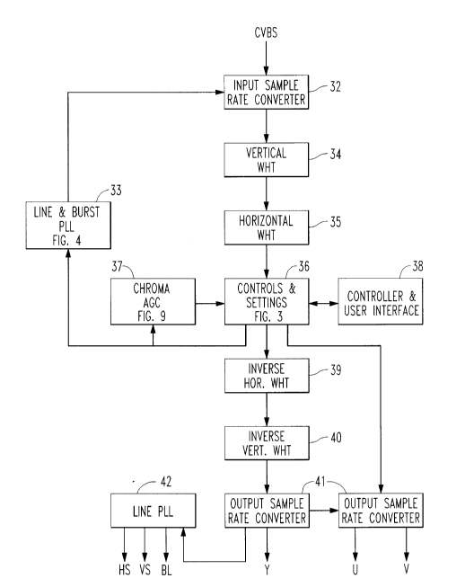
Fig. 2 A block circuit diagram of a preferred embodiment of the digital
multistandard decoder according to the invention.
Fig. 3 A circuit diagram for reali7ing the control and setting of the decoder of
Fig. 2.
Fig. 4 A circuit diagram for re:~li7ing the line/burst phase-locked loop of the
decoder of Fig. 2.
Fig. 5 A circuit diagram for reali7ing the coarse synchronous detector of the
phase-locked loop of Fig. 4.
Fig. 6 A circuit diagram for realizing the fine synchronous detector of the phase-
locked loop of Fig. 4.
Fig. 7 A circuit diagram for re~li7ing the burst phase detector of the phase-
locked loop of Fig. 4.
Fig. 8 A curve for explaining the discrimin~tor characteristics of the burst phase
detector of Fig. 7.
Fig. 9 A circuit diagram for re~li7ing the automatic gain control for the
chrominance signal.
Fig. 10 A circuit diagram for realizing a threshold/hysteresis circuit of the phase-
locked loop at Fig. 4.
Fig. 11 A circuit diagram tar re~li7ing a phase incrementing circuit of the phase-
locked loop of Fig. 4.
Fig. 12 A circuit diagram for re:~li7ing a phase integration in the phase-locked
loop of Fig. 4.
Fig. 2 shows a block circuit diagram at a preferred embodiment of she digital
multistandard decoder according to the invention. The digital multistandard decoder comprises
an input sample rate converter (SRC) 32, a line and burst phase-locked loop (PLL) 33, a vertical
2ls26s9
_ H5979,SE987
WHT circuit 34 and a horizontal WHT circuit 35, a control and setting circuit (controls and
settings) 36, a chroma automatic gain control circuit 37 (Chroma AGC), a controller and user
interface 38, a horizontal IWHT circuit 39 and a vertical IWHT circuit 40, an output sample rate
converter (SRC) 41 and a line phase locked loop (PLL) 42.
The composite signal (CVBS) e.g. digitized with the clock frequency of a host system,
such as a computer, is inputted into the input sample rate converter 32. The line and burst phase-
locked loop 33 controls the input sample rate converter 32, in the manner described hereinafter,
so that the input video signal digitized with the predetermined clock frequency is converted into
a signal with the sample values of a second virtual sampling frequency, which is tour times the
10 color subcarrier frequency. By choosing the "virtual" sampling frequency as four times the color
subcarrier frequency on the one hand the Shannon-Nyquist theorem (fa > 2-fsc) is fulfilled and
on the other an integer number of sample values per video image signal is obtained, namely 910
sample values per line for a NTSC signal and 1135 sample values per line for a PAL signal, so
that it is possible to combine the advantages at a phase-lacked architecture, in which the sampling
15 signal is an even multiple of the color subcarrier frequency, with the advantages of the line-locked
architecture, in which the sampling frequency is an integer multiple of the line frequency.
The sample values of the video signal (CVBS) at the virtual sampling frequency are then
passed onto the vertical WHT circuit 34, whose output supplies the input signals tar the following
horizontal WHT circuit 35.
In the vertical and horizontal WHT circuit 34 and 35 the input sample values of the video
signal are transformed by means of a 2x4 Walsh -H~ m~rd transformation (WHT) from the pixel
domain into the WHT domain, in which they can be processed by means at the central control and
setting circuit 36.
Each individual output coefficient at the Walsh - H~ m~rd transformation represents a
25 linear combination of all the input sample values (pixels) for said WHT, so that a single WHT
output coefficient cannot be associated with a specific input sample value. In fact a set of WHT
output coefficients reproduces the two-dimensional spectrum at all the input sample values for
a given block of a given size.
The transformation of the digitized video signal by means of a Walsh -H~d~m~rd
30 transformation into the WHT domain and the processing of the signal in the WET domain has
_ H5979,SE987 21 S2 6 S 9
proved particularly advantageous for bringing about a cost-optimized digital multistandard
decoder for video signals. Such a decoder and a corresponding digital video signal decoding
process, which makes use of the advantages of the Walsh - H~ m~rd transformation, form the
subject matter of the parallel patent application of the same applicant and the same application
5 date entitled "Video Signal Digital Decoding Process and Video Signal Digital Decoder", to
which is incorporated herein by reference.
The vertical WHT circuit essentially forms a vertical low-pass filter and a vertical
high-pass filter. in which two corresponding sample values of two video image lines are added
and subtracted, respectively. In the horizontal WHT circuit in alternating manner the high and
10 low-pass-filtered sample values of in each case one line are transformed by means of the Walsh
H~ m~rd transformation into the WHT domain. The resulting WHT matrix is inputted into the
control and setting circuit 36, in which on the one hand the chrominance signal components U
and V are separated from the luminance signal component Y and on the other all the controls and
settings of the video signal can be centrally performed in said circuit, in the manner described
1 5 hereinafter.
The WHT matrix from which the chrominance signal components were separated is then
transformed back into the pixel domain by means at the horizontal IWHT circuit 39 and the
vertical IWHT circuit 40 and the decoded video signal components U, V and Y can, optionally
following an output sample rate conversion by the output sample rate converter 41, be outputted
20 by the digital decoder.
In the digital multistandard decoder according to the invention the decoding -
demodul~ting device for the recovery of the luminance and chrominance signal components from
the video signal sample values with the virtual sampling frequency can be realized in a different
manner to that described. The processing of the video signal can take place in the pixel domain
25 (time range) or in the frequency domain with any known digital video signal decoder, which
selectively is able to process NTSC and PAL signals, the input sample rate converter 32
controlled by the line and burst phase-locked loop 33 ensuring that the standard of the particular
video signal is recognized and that the virtual sampling frequency is correctly set.
The construction and function of the circuit pa,ts of the digital decoder of Fig. 2 essential
30 for multistandard operation are described hereinafter.
2ls26s9
H5979,SE987
The heart of the digital multistandard decoder is the line and burst phase-locked loop 33,
which so controls the input sample rate converter 32 that it converts the sample values of the
video signal digitized with a first predetermined clock frequency into video signal sample values
of a second virtual sampling frequency, which is four times the color subcarrier frequency and
5 therefore 910-fh for NTSC signals and 1135-fh for PAL signals, so that the video signal can
be processed in an optimum manner in the following decoding - demod~ tin~ device. For
det~rrnining the correct virtual sampling frequency for a video signal of still unknown standard,
NTSC or PAL, the line and burst PLL 33 requires the line sync signal and burst pulse of the input
video signal (CVBS). The function at the line and burst PLL is then to lock-in the virtual
10 sampling frequency in the correct relationship and in phase-locked manner to the color subcarrier
frequency transmitted with the burst pulse.
The line sync pulse and the burst pulse of the video signal are, according to the preferred
embodiment of the invention, derived from the control and setting circuit 36, shown in detail in
Fig. 3. However, they could also be produced in some other way, known to the expert, from the
15 input video signal.
The setting and control circuit shown in Fig. 3 has four multipliers 50 to 53, which are
connected to a controller 54 and via an IC bus 55 to a user interface in the indicated manner.
Into the control and setting circuit of Fig. 3 are inputted the transformation coefficients
of the WHT matrix WHTo o to WHTo 3 and WHT~ 0 to WHT~ 3, which are formed by a 2x4
20 Walsh -H~m~rd transformation of the input sample values.
As a result of the characteristics of the Walsh - H~ m~rd transformation, whose
transformation coefficients appear as sampled values of a set of filters, the color difference signals
U and V can be directly derived as specific WHT coefficients from the control and setting circuit
36. They form the basis for the determination of the burst pulse and for synchronizing the virtual
25 sampling frequency with the color subcarrier frequency transmitted with the burst pulse.
In the case of a 2x4 WHT of the input sample values corresponding to the preferred
embodiment of the invention the color difference signals U and V can be read out directly as
WHT coefficients WHTI l and WHT, 2. They are tapped at the outputs of the multipliers 51 and
52 and supplied to the burst phase detector of the phase-locked loop 33, optionally together with
30 the control signal from the output f of the controller 54.
H5979,SE987 21 S 2 6 S 9
Unlike in known system architectures for digital decoders, in the case of the multistandard
decoder according to the invention all the control and setting functions are combined in a single
hardware stage. By means of the controller outputs a to f the WHT coefficients and consequently
the video signal to be decoded can be controlled and set.
The WHT coefficient WHTo o corresponds to a horizontally and vertically
low-pass-filtered version of the input signal and therefore is highly suitable f or the processing of
the line sync pulse of the video signal. Therefore the WHT coefficient WHTo o for sync pulse
processing (SYNC proc.) is tapped at the input of the control and setting circuit of Fig. 3.
The line and burst PLL 33 for controlling the input sample rate converter 32 is shown in
10 Fig. 4 and in detail in the following drawings. The line and burst PLL of Fig. 4 comprises a
coarse sync detector 60, a fine sync detector 61 and a burst phase detector 62. There are also a
burst gate circuit 63, a threshold/hysteresis circuit 64 and a phase increment circuit 65, as well
as a phase integrator circuit 66 and a divider 67. The connections of the individual circuit
components of the line and burst PLL can be gathered from the circuit diagram of Fig. 4, which
15 also shows the chroma automatic gain control circuit 37 (Chroma AGC).
The control of the sample rate converter via the line and burst PLL generally takes place
as follows. The virtual sampling frequency is determined in that initially the coarse sync detector
60 separates the sync pulse from the digitized video signal and establishes its time position in
order to determine the line frequency. It is then assumed that it is either a NTSC or a PAL signal.
20 For this purpose the user or m:~nuf~turer of the decoder can set default values for the sample rate
factor, depending on the particular country in which the equipment will be operated, namely at
910 or 1135.
Synchronously with the sync pulse an integral multiple of the line frequency (910-fh or
1135--fh) is produced as a first approximation of the virtual sampling frequency, the coarse sync
25 detector being set with such a wide search window that it always finds a sync pulse.
If the operation of the coarse sync detector 60 is sufficiently stable, there is a switchover
to the fine sync detector 61, which determines in a relatively narrow search window on the basis
of the approximate position of the sync pulse determined by the coarse sync detector the leading
edge of the sync pulse, i.e. the precise time position of the sync pulse and locks the virtual
30 sampling frequency precisely in the edge of the sync pulse.
12
H5979,SE987 21 S2 6 59
This prevents side-locking, which could occur in the case of only a phase-locked control
of the virtual sampling frequency relative to the phase of the color subcarrier signal during the
burst pulse.
Following stable fine phase control the phase of the color subcarrier frequency can be
5 determined by the burst phase detector 62 and the sampling frequency can be set synchronously
to this phase, the burst pulse representing a time window during which the color subcarrier
reference signal is transmitted. The thus determined, virtual sampling frequency and phase are
outputted as a control signal to the sampling rate converter 32.
The individual circuit components of the line and burst PLL of Fig. 4 and their operation
10 are described hereinafter relative to Figs. 5 to 12.
Fig. 5 shows a circuit diagram of the coarse sync detector, which determines the line sync
pulse of the video signal. Upstream of the coarse sync detector are five series-connected delay
stages 70 to 74, through which passes the WHTo o coefficient and which is then further processed
in the coarse sync detector. The circuit of Fig. 5 also comprises two comparators 75, 76, an AND
15 gate 78, a comparator 79 and a series connection of an adder 80, a binary divider 81 and a delay
element 82, which are interconnected as shown in Fig. 5.
The WHT coefficient WHTo o outputted by the horizontal WHT circuit 35 conespondsto a horizontally low-pass-filtered version of the CVBS input signal of the digital decoder. At
the end of setting and synchronization of the virtual sampling frequency the WHT coefficient
20 WHTo o corresponds to a horizontally and vertically low-pass-filtered version of the CVBS
signal. In each case WHTo 0 is used for suppressing the high frequency color subcarrier, which
would otherwise possibly disturb the detection of the line sync pulse. The limited bandwidth of
the WHT coefficient WHTo 0 which is -determined by the order of the upstream Walsh
-H~ rd transformation, also determines a nominal edge slope of the line sync pulse and
25 prevents possible peaks in the input signal.
The coefficient WHTo o forms the input signal for the line sync pulse processing. A
leading, falling sync edge is determined if the comparators 75 and 76 indicate that at least two
successive values of WHT0, 0 are higher or equal to a sync switching level (< 2-bl), a following
value of WHTo o has a random value and at least two further following values of WHT0, 0 are
30 smaller than the sync switching level (< 2--bl) The sync switching level is defined as the value
13
H5979,SE987 21 5 2 6 5 9
between the black level and the peak value of the sync pulse, as shown in Fig. lb.
In order to reduce the susceptibility to possible signal peaks and to fade out eqll~li7ing
pulses, the coarse sync detector of Fig. 5 is only active if the phase integrator exceeds a value of
"640". In this case the comparator 79 emits a " 1 " signal. If the above conditions for a falling
5 sync edge are fulfilled, then a sync trigger signal (csd%) is outputted. In addition, the difference
(csdO) of the phase integrator value with respect to the nominal number of sample values per line
(910 or 1135), as shown in Fig. 5, is stored and transferred, in order to indicate the instantaneous
phase relationship between the line sync pulse and the phase integrator for controlling the sample
rate converter. The loop gain is set by means ofthe binary divider 31 by a 12 bit offset to 1/4096.
If the coarse sync detector of Fig.5 has determined a line sync pulse and outputted a sync
trigger signal, the fine sync detector of Fig. 6 is activated in order to synchronize the virtual
sampling frequency precisely with the leading edge of the sync pulse. It forms a PI controller for
controlling the virtual sampling frequency synchronously to the line frequency of the video
slgnal.
The fine sync detector shown in Fig. 6 comprises five adders 83 to 87, two delay elements
88, 89 and two binary dividers 90, 91, shown in interconnected form in Fig. 6.
From the sum of the WHTo O values delayed by three and four clock pulses is subtracted
the sum of the undelayed WHTo O value and its counterpart delayed by five clock pulses, as
shown in Fig. 6. As the phase increments are accumulated before being inputted into the phase
20 integrator, the proportional value must be produced by means of a differentiation 86, 88, whereas
the integral value is directly accessible.
The proportional value is divided by four by a two bit shift in the binary divider 90 and
the integral value is divided by 16 by a four bit shift in the binary divider 91. By switching on
the values controlled by the sync trigger signal (csd%), which is derived from the coarse sync
25 detector, the output signal (fsdl) of the fine sync detector is generated once per horizontal line.
When the synchronization of the sampling frequency to the line sync pulse of the video
signal is termin~te~, the line and burst phase-locked loop is switched to the burst detector, which
forms a PI controller for the virtual sampling frequency relative to the color subcarrier frequency.
By means of the burst gate circuit shown in Fig. 7 and which comprises a comparator 92
30 and a counter 93 is determined a burst gate pulse. The burst gate is opened when the integer part
_ H5979,SE987 21 S26Sg
of the output signal (phint) of the phase integrator exceeds a predetermined value of "82" . The
burst gate duration is fixed on 8 clock pulses.
For the duration of the opening of the burst gate the phase of the color subcarrier signal
transmitted with the burst pulse is determined in the burst phase detector shown in Fig. 7. The
5 burst phase detector of Fig. 7 comprises four adders 94 to 97, two delay elements 98, 99 and two
binary dividers 100, 101, which are interconnected in the manner shown in Fig. 7. The input
signal is constituted by the color difference signals U and V or, in the represented embodiment
of the digital decoder, the WHT coefficients WHT, , and WHT, 2
The sum of the color difference signals is formed in the adder 94 and accumulated in a
10 register 95, which is reset at the start of the burst gate and is activated for its duration, For the
nominal burst phase of 135 the accumulated sum, as expected and necessary, passes to zero.
This value is divided by 512 by means of a nine bit shift or offset in the binary divider 101 and
subtracted from the differentiated, corresponding value, which has previously been divided by
64 by a six bit shift or offset in the binary divider 100. The result is outputted as a burst phase
15 difference (bupsd) together with the burst gate signal (bg).
Fig. 8 shows the discrimin~tor characteristics of the burst phase detector of Fig. 7 if, for
the control of the chromaticity, constant values are added to the color difference signals U and
V. This addition is performed in the adders 56, 57 of the control and setting circuit of Fig. 3,
which brings about a phase shift of the virtual burst phase.
The chroma automatic gain control circuit 37 (Chroma AGC), shown in Fig. 9, operates
in parallel with the burst phase detector 62. The Chroma AGC of Fig. 9 comprises two absolute
value elements 101, 102, two adders 104, 105, as well as two delay elements 106, 107, shown in
interconnected form in Fig. 9. Instead of adding the color difference signals U and V with their
particular signs, like the burst phase detector, the Chroma AGC of Fig. 9 accumulates the
25 absolute values of U and V while the burst gate signal is active and passes said accumulated value
to the controller. In accordance with the accumulated value the controller corrects the
multiplication factors for WHTl I and WHT~ 2 outputted at its outputs c and d (Fig. 3), so that
the output of the Chroma AGC circuit is the same as a user setting for color saturation. In
addition, a color killer signal (coki) is set under one of the three following conditions:
30 l ) if the phase-locked loop 33 (Fig. 2) is unloaded,
_ H5979,SE987 21~26S9
2) if U has the incorrect sign and
3) if the color subcarrier amplitude is too small.
This ensures that in the case of significant interference, e.g. if the incorrect video signal
standard is assumed, the chrominance components in the video signal are compressed and only
5 a luminance signal for a black and white image is outputted. The color killer signal (coki) is used
for checking whether the correct video standard has been assumed.
If coki=1, the coarse sync detector can be reactivated in order to determine the line sync
signal but then the in each case other video standard is assumed, i.e. a sampling frequency of
1135 fh is selected if previously a sampling frequency of 910-fll was selected and vice versa.
In order to avoid undesired interference and reciprocal influencing of the individual stages
of the hierarchically arranged phase-locked loop, precisely one and only one stage can be active
at a single time. The selection is made by the threshold and hysteresis circuit shown in Fig. 10.
The output signals of the coarse sync detector 60 and the fine sync detector 61 are inputted into
the threshold and hysteresis circuit 64. As shown in Fig. 10, the threshold and hysteresis circuit
15 determines different thresholds for the transition from coarse to fine phase control and for the
opposite transition from fine to coarse phase control. This ensures that once the frequency for
the virtual sampling clock has been set, the fine sync phase-locked loop can so finely tune this
frequency that a clearly defined phase coincides with a threshold level of the leading edge of the
sync pulse. When this synchronous phase relationship has been set up, then the burst
20 phase-locked loop may take over the further control. In order to avoid deadlocking, unstable or
chaotic states, only one stage of this hierarchy of the phase-locked loop may be active at a given
time and in the case of a suitable hysteresis for the tolerance for switching from one stage to the
other or for switching back into a higher-rank stage a re-liable control is ensured.
Whereas of the coarse sync detector 60, the fine sync detector 61 and the burst phase
25 detector 62 only one is always active, so that in operation there is switching from a
coarse-synchronized line PLL to a fine-synchronized line PLL and to a burst PLL, the phase
incrementing circuit 65 and the phase integrator circuit 66 are always active.
The phase increment or incrementing circuit is shown in Fig. 11 and comprises a
multiplexer device 108 and an integrator 109 constituted by an adder and a delay stage, which is
30 switched on by the burst gate signal. corresponding to the thresholds defined by the threshold
16
_ H5979,SE987 21 ~ 2 6 S9
and hysteresis circuit the multiplexer device 108 selects one of the three input signals from the
coarse sync detector 60, the fine sync detector 61 or the burst phase detector 62. The phase
increment, in accordance with the coarse, fine or burst phase different signal, is updated once
during each horizontal line, controlled by the burst gate signal, and outputted to the phase
5 integrator.
The phase integrator circuit shown in Fig. 12 comprises an adder 110 and a delay stage
111, which can be interconnected in the shown manner. The phase integrator serves as the
digitally controlled oscillator, which produces the virtual sampling frequency of 4-f s c, i.e.
910-fh or 1135-fh, for the sample rate converter. The phase integrator is timed by the burst gate
10 pulse and accumulates the phase increments determined in the preceding stage. If the
phase-locked loop is already locked in, the phase integrator accumulates increments up to an
integer value of 910 or 1135. Additionally the intermediate pixel resolution of the sample rate
converter 32 (Fig. 2), which according to a preferred embodiment ofthe invention is 1/32 (5 bits),
a non-integer output of the phase integrator. The phase integrator circuit requires in the
15 represented embodiment an overall resolution (precision) of 29 bits, 12 bits being required for
the integer and 17 for the non-integer integrator output values.
As shown in Fig. 12 the sync trigger signal outputted by the coarse sync detector resets
the integer bits of the accumulator, but the non-integer bits remain unaffected.
The carry of the phase integrator, i.e. the carry from the non-integer to the integer
20 components, determines a time at which a given sample value for a sampling frequency of 4--f
s c, is to be calculated by the input sample rate converter. The non-integer component of the
output signal of the phase integrator specifies the intermediate pixel distance of the "virtual"
sample value from an actual sample value as fractions of the host clock frequency.
However, the sample rate converter requires a control input value, relative to the output
25 sampling rate (4-f s c) . As the phase increment indicates the relationship of the host clock
frequency to 4-fs c~ it is necessary to divide the non-integer component of the output value of the
phase integrator by the value of the phase increment. This division is performed by the divider
67, The accuracy of this division must enable the sample rate converter to produce intermediate
pixel increments of 1/32 (5 bits) . In order to form an output signal with a precision of 5 bits, the
17
- H5979,SE987 21 5 2 6 ~ 9
input precision of the divider must be 7 bits for the numerator and 8 bits for the denominator.
The input sample rate converter 32 can be in accordance with the prior art. A particularly
simple and advantageous sample rate converter suitable for digital multistandard video decoders
is described in the parallel application of the same applicant and having the same application date
5 entitled "Sample rate converter and sample rate conversion process" to which is incorporated
herein by reference, Such a sample rate converter performs an equally weighted interpolation
between each of two neighboring sample values and subjects to an amplitude correction the
interpolation result obtained. Then a further equally weighted interpolation of the corrected, first
interpolation result is performed with its neighboring values and these can be neighboring sample
10 values or neighboring interpolation results and the interpolation result obtained then again is
subject to an amplitude correction. The equally weighted interpolation is then repeated until the
desired resolution necessary for the virtual sampling frequency is reached, e.g. 1/32 of the host
clock frequency. The control signal for the sample rate converter outputted by the phase-locked
loop then determines the direction and magnitude of an offset for in each case one virtual sample
15 value relative to an actual sample value.
At the output of the digital multistandard decoder according to the invention can once
again be provided a sample rate converter controlled by a line and burst PLL, if the decoded video
signal is to be further processed at a clock frequency other than 4-f 5 c
However, it is also possible to provide a simplified output sample rate converter 41
20 controlled by a line phase-locked loop 42 (Fig. 2) In the line PLL corresponding parts of the
described line and burst PLL, namely the coarse and fine sync detectors are repeated, said parts
being copied for the line PLL, but cannot be directly reused, because they must continuously
monitor the burst PLL. For the output sample rate converter it is possible to use a simple linear
interpolation between adjacent pixels, because only baseband signals Y, U and V and not
25 composite video signals (CVBS) have to be processed, which with the color carrier frequency
contain information with a high spectral component, which occurs after demodulation as a d.c.
voltage. The requirements made concerning the linearity of the frequency-dependent gain
function of the sample rate converter are therefore much less.
The invention relates to a digital multistandard decoder for composite video signals. The
18
_ H5979,SE987 2 1 $2 6 ~ y
multistandard decoder according to the invention can selectively process NTSC or PAL video
signals. It comprises a sample rate converter, which converts the sample values of the video
signals digitized with a first predetermined clock frequency into video signal sample values of
a second virtual sampling frequency, has a phase-locked loop for controlling the sample rate
5 converter, a sync detector, in order to determine the line sync pulse and set the virtual sampling
frequency to an integer multiple of the line frequency of the video signal, and a burst detector in
order to set the virtual sampling frequency synchronously with the phase of the color subcarrier
signal of the video signal, and a decoding -demod~ ting device.
19