Note: Descriptions are shown in the official language in which they were submitted.
2~.~~"~~~
DF-2855
Inventor: Matthew Simpson
SYNTHESIZING DIAMOND FILM
FIELD OF THE INVENTION
This invention relates to synthetic diamond and, more
particularly, to a method of making synthetic diamond film.
BACKGROUND OF THE INVENTION
Diamond has a number of properties which make it attractive
for use as window material, free-standing domes, or other planar
and non-planar structures for various applications. Among these
properties are extreme hardness and excellent transmissivity of
certain radiation. Diamond is also an extraordinary heat
conductor, thermally stable, and an electrical insulator.
However, natural diamond is prohibitively expensive for
applications which require any substantial size and is difficult
to form into certain shapes.
In recent years, a number of techniques have been developed
for depositing synthetic diamond on surfaces of various shapes to .
obtain a diamond film or coating on tool surfaces and devices.
These techniques include so-called high-pressure high-temperature
1
~1~~"~69
("HPHT") methods and. chemical vapor deposition ("CVD") methods.
The CVD methods include plasma deposition techniques wherein, for
example, plasmas of a hydrocarbon and hydrogen are obtained using
electrical arcing. The resultant plasma can be focused and
accelerated toward a substrate using focusing and accelerating
magnets.
In order to obtain diamond films having shapes needed for
particular applications, it is desirable to have substrates for
diamond deposition that can be readily formed into the
IO appropriate shapes. Graphite is such a material, and synthetic
diamond film has been deposited, such as by chemical vapor
deposition, on the surface of a graphite substrate. If
necessary, the graphite can then be removed, leaving a free-
standing diamond film or layer of a desired 'shape. Graphite can
be provided that has a coefficient of thermal expansion that is
relatively close to that of diamond film, and in this respect it
is favorable for deposition of diamond film. However, diamond
film generally does not deposit well on graphite because diamond
deposition conditions tend to etch graphite, which leads to
erosion of the substrate rather than deposition. .
It was previously discovered that deposition of synthetic
diamond on a graphite substrate can be improved by providing a
a a-
thin interiayer of a metal, particularly molybdenum or tungsten.
The thin layer of the metal was found to facilitate the adherence
of the synthetic diamond being deposited. Although the metal
2
2~~~~~~
does not hatch well with the diamond from the standpoint of
thermal coefficient of expansion, use of a very thin layer of the
metal minimizes the impact of such mismatch.
While coatings or interlayers of metals such as molybdenum
or tungsten on graphite have been found to be generally
effective, there is room for further improvement.
It is among the objects of the present invention to devise
improvements in techniques for deposition of synthetic diamond
film on graphite substrates.
3
~1~~'~ ~~
SUMMARY OF THE INVENTION
Applicant has discovered that carbon-containing compounds
(which, for purposes hereof, means solid compounds that are
thermally stable above at least 500°C and contain between 10 to
90 atomic% carbon), and especially silicon carbide, provides an
advantageous and relatively inexpensive interlayer for CVD
deposition of synthetic diamond on graphite. Applicant has also
discovered that the degree to which the synthetic diamond adheres
to the coated graphite surface can be controlled by varying the
carbon content of the carbon-containing compound from which the
interlayer is formed. In particular, when the interlayer is
relatively rich in carbon (as compared to the stoichiometric
compound), the synthetic diamond has relatively less adherence to
the coated substrate, whereas when the interlayer is relatively
lean in carbon (as compared to the stoichiometric compound), the
synthetic diamond has relatively greater adherence to the coated
graphite.
In accordance with an embodiment of the invention, there is
disclosed a method of making a diamond film, which includes the
steps of: providing a graphite substrate; forming a layer of a
carbon-containing compound on a surface of the substrate; and
depositing a synthetic diamond layer on the layer of carbon- ''
containing compound.
In a preferred embodiment of the invention, the layer of a r-
4
~1~~~~~
carbon-containing compound comprises a layer of silicon carbide.,
In this embodiment, the layer of silicon carbide is formed to a
thickness in the range to a 25 to 250 Vim.
In accordance with a further feature of the invention, the
~ step of forming said layer of carbon-containing compound
comprises controlling the carbon content of said compound to
adjust the adherence of said diamond layer on said layer of
carbon-containing compound. The carbon content of the compound
is preferably controlled to be rich or lean in carbon by at least
1 at% above or below, as the case may be, the stoichiometric
carbon content.
Further features and advantages of the invention will become
more readily apparent from the following detailed description
when taken in conjunction with the accompanying drawings.
5
~1~~~~~
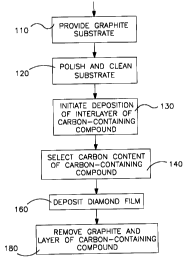
BRIEF DESCRIPTION OF THE DRAWINGS
Fig. 1 is an operational flow diagram of the steps of an
embodiment of the method of the invention.
Fig. 2 illustrates a structure made in accordance with an '
embodiment of the invention.
Fig. 3 is a schematic diagram of a plasma jet deposition
system which can be utilized for CVD deposition of synthetic
diamond for use in an embodiment of the method of the invention.
6
DETAILED DESCRIPTION
Referring to Fig. 1, there is shown, an operational flow
diagram of steps that can be utilized to produce synthetic
diamond film in accordance with an embodiment of the invention.
The block lI0 represents the providing of a graphite substrate.
Preferably, the graphite material will have a relatively small
pore size, for example a maximum pore size less than about 10
microns. Also, the graphite chosen should preferably have a
coefficient of thermal expansion which substantially matches
synthetic diamond. The graphite substrate can be machined or
otherwise formed into a desired shape. The block 120 represents
the polishing and cleaning of the substrate surface upon which
diamond film is to be deposited. Polishing can be implemented,
for example, by lapping, and the surface should preferably be
polished smoother than the pore size. The polished substrate
surface can then be cleaned using an ultrasonic cleaner. Next,
as represented by the block 130, the deposition of a layer or a
carbide-containing compound, preferably silicon carbide, is
initiated on the prepared graphite surface. The layer should
preferably be continuous, free of pores, and seal off the pores
of the polished graphite surface. It should also be relatively
thin, to minimize thermal mismatch stress with regard to the ''
diamond to be subsequently deposited. The preferred thickness is
in the range 25 to 250 microns. The silicon carbide adheres well
7
~1~~7~~
to graphite, and good quality synthetic diamond can be deposited
thereon. The silicon carbide layer can be deposited by any
suitable means, for example, vapor deposition, such as CVD.
Depending on the shape, thickness, and other characteristics
of the diamond to be deposited, as well as deposition parameters,
it may be desirable to increase or decrease adherence of the
diamond being deposited, in order to encourage or discourage
release of the diamond at a particular stage of the deposition
process (if the diamond is to be released) and to maximize the
probability of obtaining intact diamond film. In accordance with
a feature of the invention, the carbon content of the interlayer
compound is selected to adjust the relative adherence of the
synthetic diamond to be deposited thereon. It is the surface of
the interlayer that largely controls adherence of the diamond, so
the control of carbon content of the interlayer compound for the
surface portion thereof, particularly the last 5 nm thereof, is
more significant than the carbon content of the interlayer
material below. In Fig. l, the block 140 represents selection of
the carbon-content of the interlayer carbon-containing compound,
particularly the surface portion thereof.
The block 160 represents the deposition of a diamond film
over the layer of silicon carbide. The diamond film is
preferably deposited using a chemical vapor deposition (CVD) ''
technique, for example the plasma jet deposition technique
described in conjunction with Fig. 3. If desired, the deposited
8
2~~~~~~
, diamond film, if not previously released, can then be removed ,
from the substrate and the interlayer, such as by grinding away
the graphite and removing the interlayer (block 180).
Fig. 2 illustrates the structure of a graphite substrate 10
(shown planar, although it can be any shape), the carbon-
containing interlayer compound 30, and the synthetic diamond
layer 50.
There are various ways by which the silicon carbide
interlayer of the present can be formed. One such technique is
to flow mixtures of halosilanes (e. g. SiCl4), hydrocarbons (e. g.
CH4) and hydrogen over the graphite to be coated, which is heated
to a temperatures of order 800C. Control of the composition of
the material being deposited can be achieved by varying the ratio
of Si to C in the feed gases. Alternatively, the graphite to be
coated can be heated in an atmosphere containing silicon in a
vapor form. The silicon is allowed to condense and react with
the surface carbon to form SiC. In this technique, altering of
the temperature can be used to affect the coating composition. A
lower temperature will result in a coating richer in Si.
Referring to Fig. 3, there is shown a diagram of a plasma
jet deposition system 200 of a.type which can be utilized in
practicing an embodiment of the invention. The system 200 is
contained within a housing 2i1 and includes an arc-forming ~'
section 215 which comprises a cylindrical cathode holder 294, a
rod-like cathode 292, and an injector 295 mounted adjacent the
9
2~~~~~~
cathode so as to permit injected fluid.to pass over the cathode
292. A cylindrical anode is represented at 291. In the
illustrated system the input fluid may be a mixture of hydrogen
and methane. The anode 291 and cathode 292 are energized by a
source of electric potential (not shown), for example a DC
potential. Cylindrical magnets, designated by reference numeral
217, are utilized to control the plasma generated at the arc
forming section. The magnets maintain the plasma within a narrow
column until the hot gases reach the deposition region 60.
Optional cooling coils 234, in which a coolant can be circulated,
can be located within the magnets.
In operation, a mixture of hydrogen and methane is fed to
the injector 295, and a plasma is obtained in front of the arc
forming section and accelerated and focused toward the deposition
I5 region. The temperature and pressure at the plasma formation
region are typically in the approximate ranges 1500-15,000
degrees C and 100-700 torr, respectively, and in the deposition
region are in the approximate ranges 800-1100 degrees C and
0.1-200 torr, respectively. As is known in the art, synthetic
polycrystalline diamond can be formed from the described plasma,
as the carbon in the methane is selectively deposited as diamond,
and the graphite which forms is dissipated by combination with
the hydrogen facilitating gas. Far further description of plasma
jet deposition systems, reference can be made to U.S. Patent No.s
4,471,003, 4,487,162, and 5,204,144. It will be understood that
CA 02152769 1999-02-24
other suitable types of deposition equipment, including other
types of CVD plasma deposition equipment, can be used in
conjunction with the features of the invention.
The bottom portion 105A of the chamber has a base 106 on
which can be mounted the graphite substrate 10 with the silicon
carbide interlayer 30 on which the synthetic diamond is to be
deposited. Reference can be made, for example, to U.S. Patent
5,314,652 issued 24 May 1994 assigned to the same assignee as the
present Application, which describes considerations of roughness
of the substrate with regard to appropriate holding and release
of the diamond during and after deposition. The base can include
a temperature controller. It will be understood that other
diamond deposition techniques can be used. The substrate can be
tilted and rotated during deposition as described, for example,
in U.S. Patent No. 5,204,144.
TV T 1/TT T' 1
A disk l2cm diameter by l.2cm thick was fabricated from
IG-11 graphite. The disk was coated with SiC using a vapor phase
process, but at the end of the process, the proportion of C was
adjusted to be higher than that required to achieve the SiC
stoichiometry. Diamond was deposited on the coating substrate
11
2~.~2'~~:~
under the following conditions:
Deposition temperature: 925
Pressure: 7.3 torr
Enthalpy: 45-53 kJ/g
%CH4: 0.1°s
until the diamond reached a thickness of about 50um. The run was
stopped and the diamond detached from the coated substrate,
permitting the coated substrate to be used again. The silicon
carbide coating for this example was analyzed by EDAX (energy
IO dispersive analysis of x-rays) in an electron microscope and
compared to a sample whose composition was at SiC stoichiometry.
The K-alpha Si peak was reduced in intensity relative to the
standard by 7.4%, suggesting that the silicon content of the
surface layer was at least 7.4°s lower than stoichiometric SiC;
i.e., the C content was at least 53.7 ate.
r, ~, w »r~ r c~ ~f
A disk l2cm diameter by l.2cm thick was fabricated from IG-
11 graphite. Three fine grooves were machined into it at radii
of 5, 5.3, 5.6cm. The grooves were less than lmm wide and deep
and served to arrest the propagation of cracks from the edge into
the center. The disk was coated with SiC using a vapor phase
process, but at the end of the process, the proportion of Si was a.
adjusted to be higher than that required to achieve the SiC
stoichiometry. Diamond was deposited on the coated substrate
12
21~2'~~~
under the following conditions:
Deposition temperature: 1025-1080
Pressure: 15 torr
Enthalph: 43 kJ/g
% CH4: 0.15%
until the diamond reached a thickness of about 200um. The run
was stopped and the diamond remained firmly adhered to the
substrate. The diamond was examined and no cracks were found in
it. The silicon carbide coating for this example was analyzed by
EDAX (energy dispersive analysis of x-rays) in an electron
microscope and compared to a sample whose composition was at SiC
stoichiometry. The K-alpha Si peak was 26.8% more intense than
the standard, suggesting that the silicon content of the surface
layer was at least 63.4 at%.
EXAMPLE 3
A disk 12 cm dia by l.2cm thick was fabricated froma grade
of graphite with expansion similar to IG-11 and coated with
silicon carbide using the second of the two above-described
methods. Diamond was deposited on the coated substrate under the
following conditions.
Deposition temperature: 1000C
Pressure: 8.5 torr
Enthalpy: 35 kJ/g
%CH4: 0.1% 'w
At the end of the run, a diamond coating at least 200um thick was
formed on the substrate. It The run was stopped and the diamond
13
2~~2~~~
remained firmly adhered to the substrate. The diamond was
examined and no cracks were found in it. The coating of this
example had a rougher surface than the coatings of the two
previous examples, precluding a guantitative EDAX analysis.
Qualitatively, the composition appeared closer to the SiC
standard than the other two coatings. No other elements were
detected at significant levels. Visually, the coating for
example 3 looked greenish, which color is associated with
relatively pure silicon carbide (Kirk-Othmer Encyclopedia of
Chemical Technology, vl, p33). From this and from the EDAX
analysis, we conclude this coating was close to pure SiC and
hence has composition 50 at% Si, 50 at% C. The coating for
example 2 (silicon rich) had a silvery color and the coating for
example 1 (carbon rich) appeared darker than example 2, but still
I5 shiny. No color was evident in either coating.
14