Note: Descriptions are shown in the official language in which they were submitted.
CA 02152781 2003-08-07
DIGITAL DEI~iODULATOR 8IT8 FREQUENCY
aND TIRING C0~1TROL
Field of the Invention
The present invention relates generally to the
demodulation of digital signals and more particularly to the
demodulation of quadature phase shift keyed (QPSK) signals.
Background of the Invsntion
Presently, the design of commercial cordless
telephone systems is based primarily on analog signal
processing and transmission techniques. The use of digital
techniques in other transmission systems have resulted in
improved system performance due to a reduction in signal
interference and noise achieved using digital techniques. It
is, therefore, desirable to incorporate digital signal
processing and digital transmission techniques in the next
generation cordless telephones.
Such cordless telephone systems typically include a
battery powered portable station (handset) and a base
station. The base station is optimally connected to other
telecommunication networks. Although the invention may be
used in any digital transmission system, its use will be
described herein for application in digital cordless
telephone (DCT) systems.
Communication channels between the handsets and
base stations in DCT systems may be set up using slotted
WO 94/16512 PCT/US93112697
~~~~~i8'~
- 2 -
ALOHA, a well known TDMA (time division multiple access)
technique. The DCT system may communicate, for instance,
using TDD (time division duplexing) for transferring
information between the handsets and the base station. It is
typical in such systems to operate in both burst and
continuous modes. The burst mode is generally used to
broadcast messages and to transmit control information, i,e.
to set up a link between the base station and a particular
handset. Once all of the control functions have been
performed to set up a link, data, i.e. voice data, may be
transmitted using a series of continuous bursts, referred to
as the continuous mode.
A common form of digital communication employs a
digital modulation technique known as Phase Shift Keying
(PSK). In PSK, the phase of a carrier signal is switched
between two or more values in response to binary data
representing the information to be communicated. Where only
two transmit phases are provided, each phase represents a
single binary digit. For instance, the carrier signal can be
switched so that its phase is 180° in response to a binary
"1" and switched to 0° in response to a binary "0". This
technique is known as phase reversed keying (PRK). The PRK
waveform can be written as
~~ (t) - A sin(w~t) (1)
~2(t) - -A sin(c~~t) (2)
where c~~ is the angular frequency of the carrier and ~~ and
are the phases of the PRK signal. The PRK waveform according
to equations (1) and (2) is shown in Fig. 1.
To increase bandwidth efficiency (the number of
bits transmitted per unit of time), a technique known as
quadature PSK (QPSK) is used. In QPSK each transmit phase
represents two bits of data thereby increasing the amount of
data that can be transmitted over each phase interval. The
advantage of QPSK modulation is that both the in-phase (I)
and the quadature (Q) portions of the carrier signal can be
modulated and combined to form the QPSK signal. For
instance, Fig. 2a. shows an unmodulated phaser of the carrier
~. 5 2 '~ ~' 1_ j ~P ~ T us 9 _ '. ' ~ ~ ~. '~ ~
n'
IPEAIt~4:
- 3 -
signal. Fig. 2b and Fig. 2c show the modulated carrier of
each the I and Q portions of the carrier signal respectively.
The QPSK signal can be represented by:
~1 = A c:os ( c~~t. )
~2 = -A sin (w~t) (4)
~3 - -A COS ( (.~~t ) ( 5 )
~4 - A sin (c~~,t) (6)
The phaser diagram shovan in Fig. 2d results from the
combination of the I and Q portions of the carrier signal.
Fig. 3 :is a block diagram of a prior art coherent
QPSK demodulator. As :shown, the QPSK carrier signal is
received and filtered by bandpass filter 500. Filter 500
rejects undesirable adjacent channel interference and thermal
noise. Typicall;r, automatic gain control (AGC) 502 is
utilized to adjust the energy level of the received signal.
In a TDMA.system,. larg(~ burst-to-burst level differences
arising from downlink :Fading due to atmospheric attenuation,
distance and scattering can vary significantly. Thus AGC 502
detects the peak power of the received signal and provides
feedback to the receiver so that the receiver's amplifier
levels can be adjusted according to the strength of the
received signal. Power divider 504 is provided to compensate
for the power level difference in the carrier phase and bit
timing recovery circuits 506 and 508 respectively.
The carrier phase recovery circuit 506 extracts the
I and Q signal components from the received PSK signal. The
90° hybrid circuit 510 is used to separate the I and Q
signals. To this end, the I signal is mixed with the cos
(c~~t) and the Q :signal is mixed with the sin(w~t)
by mixers 514 a:nd 512 respectively. Integrators 518 and 516
are used to dete~~t the energy of the down converted signal
over each time interval according to a well-known
relationship:
E ~t~21 f ( t) ~dt , - (~)
. f . . r
~~ a~'~~1
Eai ' ~ 9 ~ ~~ .~.- ~7
4 -
where f(t) is the signal (i.e., ideally f(t) - ~1, ~2, ~3 or
~4 over the interval t1 to t2) and E is the energy of the
signal over the i:ime interval t1 to t2. Since there are two
transmit phases :Eor each of the I and Q signals and they are
separated by a 130° phase shift, the phase of the signals
over a given timf=_ interval is either + E or -E as shown in
Figure 4.
Figure 4 shows that when the detected energy of the
in-phase signal is -E, the probability that the received
l0~signal corresponds to 'transmit phase ~2 (equation 4) is
greatest and when the detected energy of the in-phase signal
is +E the probability that the received signal corresponds to
transmit phase ~4 (equ,ation 6) is greatest. Similarly,
Figure 4 shows that when the detected energy of the quadature
signal is -E, the probability that the received signal
corresponds to ~:3 (equation 5) is greatest and when the
detected energy of the quadature signal is +E, then the
probability that the received signal corresponds to ~1
(equation 3) is greatest.
Referring again to Fig. 3, I and Q decision
circuits 520 and 522 determine the transmit phase of the
received signal .and reconstruct the transmit data, i.e. the
binary data represented by the phase of the signal. The
reconstructed binary data output from the decision circuits
520 and 522 is then combined into a single serial stream of
binary data by t:he parallel-to-serial converter 524.
In most transmission systems, including DCT
systems, communisation between a receiving unit and a
transmitting unit requires burst synchronization. Such
synchronization is typically accomplished by providing the
demodulated binary data to a correlator which detects a known
pattern, such as a predefined preamble. Detection of the
preamble or other known pattern allows the demodulator to
synchronize its timing with the received PSK signal so that
the demodulator can decode the received symbols.
It is well known to fine tune the demodulator's
timing to the received symbols during operation in a
P.ME~ID~D JH~.T
WO 94/16512 ~ PCT/US93/12697
- 5 -
continuous me>de to optimize system performance and reduce
error. Such fine tuning may be provided by the symbol timing
recovery circuit 508 shown in Figure 3. A typical symbol
timing recovery circuit would determine within which time
intervals the: maximum amount of energy is received. Those
intervals should correspond to the symbol intervals of the
received signal. Thus the symbol timing recovery circuit 508
causes the decision circuits 520 and 522 to determine the
phase of the received signal so that the decision corresponds
to only a single symbol.
It has been found that the analog demodulator of
Fig. 3 can be simp7.ified by digitizing the integration and
decision functions. Fig. 5 is a block diagram of such a
digital demodulator.
After demodulating the received signal using mixer
530, the PSK signal. is sampled at a frequency greater than
twice the Nyquist frequency, where the Nyquist rate is the
highest frequency of the down converted PSK signal. It has
been found that by determining the zero-crossings of the
signal with respect. to time and referencing the zero-crossing
to a reference transmit phase, the phase of the received
signal can be determined. Waveform digitizer 532 samples the
down converter signal represented in Figure 5 generally at
536. The zero-crossing digital signal processor (DSP) 534
estimates the ~°ro-crossings of the sampled waveform and then
compares them to ~ch.ose of each of the possible transmit
waveforms to ~determ.ine the phase of the received signal.
However, this technique can become quite
complicated due to the iterative curve fitting for
trigometric functions which is necessary to determine the
phase of the :received signal. Furthermore, noise,
intersymbol interference, and timing misalignment degrade the
received signal sa that only a best curve rather than an
exact curve can be identified.
To avoid these problems, a phase progression
digitizing technique has been suggested. This technique
bypasses the waveform digitizer 53~> and the complicated zero-
WO 94/16512 PCTIUS93I12697
- 6 -
crossing DSP 534 by directly digitizing the signal phase.
This technique uses a counter to count each cycle of the
received PSK signal, either on up-crossings or on down-
crossings. A fixed sample rate is selected to be at least
equal to the Nyquist rate of the modulation, i.e. at least
twice the symbol rate. optimally a number of cycles will
occur between samples. The samples mark events, i.e., an up-
crossing or down-crossing, in time. Thus the phase of the
received signal is determined by comparing the time of the
events occurring in each symbol period.
For example, consider the phase progression plot
shown in Fig. 6. The phase progression plot plots the events
as a function of time. The PSK signal is shown below the
plot. The samples or events are enumerated as well as the
time of each event. The curve fit for determining the phase
of each symbol becomes a system of parallel lines where each
line corresponds to one of the possible transmit phases.
Using this technique all amplitude information is discarded
and trigometric curve fitting can be avoided.
Unfortunately, this technique has several
limitations as well. In particular, the sampling frequency
in such a scheme is critically linked to the signal frequency
in that a sample must occur on either upward zero-crossings
or downward zero-crossings. Thus, whenever the signal
undergoes frequency drift, which is well know to occur in
communication systems, or frequency changes for other
reasons, the sample rate will require constant adjustment to
track such frequency changes.
Accordingly, a need still exists for a digital
demodulator which can detect the phase of the received signal
regardless of frequency changes and drift of the received PSK
signal, which is relatively inexpensive and simple to
implement.
summary of the Invention
The present invention fulfills this need by
providing a digital demodulator and a method for demodulating
digital data. According to the present invention, the
WO 94/16512 ~ PCT/US93/12697
digital demodulator comprises a phase detector which accepts
an input of digital data formed by sampling a received analog
PSK signal and converts the digital data into phase estimates
based on transitions in the digital data. The phase
estimates are then converted to phase data indicative of the
transmitted .information by a data decoder.
In a preferred embodiment the digital data is
grouped into overlapping windows of data. The digital
demodulator according to this preferred embodiment comprises
a unique word detector, a timing recovery controller, and a
frequency controller. The decoded data is output to the
unique word detector which correlates the decoded data with a
predefined unique word. When the unique word has been
detected, them unique word detector outputs a signal
indicating within which of the overlapping windows the unique
word had been detected.
The frequency controller monitors the phase
estimates provided by the data decoder and compares them with
the closest of the possible transmit phases to determine a
phase error. Since a change in phase error over a symbol
interval is indicative of frequency drift, the frequency
controller determines a frequency offset from time to time to
track the frequency of the received PSK signal.
The timing recovery controller uses the frequency
offset to adjust the phase error G.termined after each symbol
period. If the symbol timing of the demodulator was
synchronized with the timing of the received symbols, the
phase error would approach zero. When the phase error,
however, is greater than some predetermined threshold, the
timing of the demodulator must be advanced or delayed to
synchronize with the timing of the received symbols. The
timing recovery controller comprises early and late counters
for maintaining a count related to the phase error in an
early window and a late window respectively. When the phase
error in the early counter is greater than the phase error in
the late coun~~er the timing of the demodulator is advanced
and when the phase error in the late counter is greater than
CA 02152781 2003-08-07
_ g _
the phase error in the early counter the timing of the
demodulator is delayed.
In a further preferred embodiment, the phase detector
comprises an instantaneous phase decoder, instantaneous phase
estimator, and a differential decoder if the transmitted
signals are differentially encoded. The instantaneous phase
decoder identifies when transitions occur in the digital
data. The instantaneous phase estimator estimates, based on
when the transitions occur, the instantaneous phase of the
received signal and averages a number of instantaneous phase
estimates together. The differential decoder computes the
phase difference between consecutively received symbols based
on the phase estimates corresponding to windows having the
same timing.
In still another preferred embodiment, the digital data
is formed by limiting the received analog signal and sampling
the limited signal thereby removing substantially all
amplitude characteristics from the received PSK signal prior
to demodulation.
In one aspect, the invention provides in a digital
communications system having a transmitter for transmitting
information in the form of an analog phase shift keyed (PSK)
signal and a receiver for receiving said PSK signal, said PSK
signal having amplitude, frequency, and phase characteristics
wherein at least some of said phase characteristics are
related to the information so transmitted, a demodulator
comprising; a phase detector receiving an input of digital
data representative of said analog PSK signal so received and
providing successive outputs representative of phase
estimates of said PSK signal based on transitions in said
digital data; and a data decoder having an input coupled to
said phase detector to receive an input of said phase
estimates, said data decoder converting said phase estimates
to phase data indicative of said transmitted information.
CA 02152781 2003-08-07
- 8a -
In another aspect, the invention provides a method for
demodulating a phase shift keyed (PSK) signal having a
sequence of symbols, each symbol being based upon one of a
known set of possible transmitted phases, said symbols being
received in succession by a receiver, comprising the steps
of: generating an analog signal indicative of the symbols
received by the receiver and defining the analog signal as
said PSK signal; digitizing said PSK signal to provide a
sequence of digital data samples representative of said PSK
signal received, each digital data sample having a value
associated with one of a high level and a low level;
identifying transitions from said high level to said low
level and from said low level to said high level between
successive digital data samples; generating a phase estimate
based on said transitions so identified; and decoding each
phase estimate to provide binary data representative of said
symbols received and defining said data as decoded data.
Brief Description Of The Drawings
The present invention will be better understood, and its
numerous objects and advantages will become apparent by
reference to the following detailed description of the
invention when taken in conjunction with the following
drawings, in which:
Figure 1 graphically represents a PRK waveform;
Figure 2 shows a phaser diagram of a QPSK signal;
Figure 3 is a block diagram of a QPSK demodulator
according to the prior art;
Figure 4 shows energy detection envelopes of QPSK
symbols;
Figure 5 is a block diagram of a prior art digital PSK
demodulator;
Figure 6 is a phase progression plot of a PSK waveform;
WO 94/16512 ~ PCT/US93/12697
~152'~81
_g_
Figure 7 .is a block diagram of a digital
demodulator according to the present invention;
Figure 8 :shows the signal input to and signal
output from a limit:er amplifier;
Figure 9 is an example of a window/symbol timing
using four windows per symbol period;
Figure 10 is a timing diagram showing a desired
timing adjustment for fine tuning demodulator
synchronization;
Figure 11 is a block diagram of a preferred
embodiment of a phase detector according to the present
invention;
Figure 12 is a block diagram of a preferred
embodiment of an instantaneous phase decoder;
Figure 13 is a block diagram of a preferred
embodiment of an instantaneous phase estimator according to
the present invention;
Figure 14 is a block diagram of a preferred
embodiment of a differential phase detector according to the
present invention;
Figure 15 is a block diagram of a preferred
implementation of the instantaneous phase estimator,
differential detector and data decoder according to the
present invention;
Figure 16 graphically depicts a symbol pha~~ shift
of nearly 360° with reference to a synchronizing window
according to 'the present invention;
Figure 17 shows an exemplary sequence of digital
data and denotes transitions occurring within that sequence;
Figure 18 graphically depicts quadrant and octant
mapping for a ~r/4 QPSK signal according to the present
invention;
Figure 19 is a block diagram of a preferred
embodiment of an automatic frequency controller according to
the present invention;
~~i2'~~1 ~ ~cTUsg3l=~~~
r
I E~;/ 4 ~: . ova
- 10 -
Figure 20 is a block diagram of a preferred
implementation of the automatic frequency controller
according to the present invention;
Figure 21 is a block diagram of a preferred
embodiment of an automatic timing recovery controller
according to the present invention;
Figure 22A is. a flowchart of the AFC and ATRC
software routine according to the present invention;
Figure 22B is. a flowchart of the ATRC software
routine according to the present invention; and
Figure 23 is a block diagram of a preferred
embodiment of a unique word detector according to the present
invention.
Detailed Description
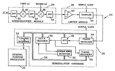
Fig. 7 shows a block diagram of a portion of a
radio frequency (RF) receiver/signal processor, generally
designated 20, including a digital demodulator constructed in
accordance 'with the present invention. Such a receiver has
the advantages of low cost, low complexity and low power
consumption. The overall function of the receiver is to
recover digital data from an analog input signal (IF IN) and
pass such digital data to a central processor 22. IF IN, in
the preferred embodiment, is a ~r/4 differential coded
quaternary phase shift keyed (DQPSK) signal in analog form.
IF IN is an analog transmission representative of various
phase represented symbols. IF IN is transmitted at a given
symbol rate. Each phase symbol is representative of a set of
digital data, i.e., a particular bit sequence. Although the
arrangement shown in F'ig. 7 is a combination analog/digital
device, it is susceptible to an integrated circuit
implementation.
Receiver 20 is shown to generally include a down
converter module 24, a. limiter module 26 and a demodulator
module 28. Down converter 24 serves to down convert IF IN
from a received frequency of approximately 25~ MHz to a low
IF signal of approximately 1.152 MHz. Limiter 26 serves to
both limit the low IF signal or down converted signal and
__.._. dllt mcn...ca. ~.-z _...y..~..~...~._-..-__W....-
.__~_~~,..._.._._e~_..~._._K.-~.w
CA 02152781 2003-09-08
11 -
sample the signal at a sample rate which is at least the
Nyquist rate of the down converted signal.
Demodulator module 28 recovers a differential phase
signal from the samples generated by limiter 26. Such
recovery occurs by removing frequency and phase error to
optimize the detection of phase information from the
differential phase signal. Once differential phase
information is recovered from the down converted signal,
phase symbols can be determined and converted into actual
l0 digital data output to processor 22.
Down converter module 24 is shown to include
bandpass filters 30, 32 and 34 and mixers 36 and 38. Filter
30 eliminates out-of-band signals, including spurious mixing
images and other channel transmissions, if any, reduces
noise, and shapes the desired signal. Filter 30 exhibits a
response roughly approximating an optimal "matched" filter to
a filter used prior to transmission.
It will be appreciated that the down conversion of
IF IN is achieved by passing the signal through mixers 36 and
38. Although the actual frequencies selected for the first
and second signals applied to mixers 36 and 38, respectively,
can be any frequency which will achieve the necessary down
conversion, certain frequencies are preferred because of
their non-interference characteristics. A more detailed
2 5 explanation of the frequencies selected and the
considerations relating to such selection may be found in
U.S. 5,722,040. In the preferred embodiment mixer 36 down
converts IF IN to approximately 10.7 MHz.
Filter 32 generally performs the same function as
3o filter 30, namely image rejection, noise rejection and signal
shaping. Mixer 38 provides the final down conversion of IF
IN to approximately 1.152 MHz. Filter 34 is a discrete
inductor-capacitor (LC) filter which primarily eliminates
mixing products occurring during the down conversion process.
WO 94/16512 PCT/US93/12697
21x2781
- 12 -
The primary function of limiter 26 is to convert
the down converted and filtered IF IN analog signal, output
from filter 34, into a digital signal without the use of an
analog-to-digital converter. The digital signal generated by
limiter 26 is thereafter provided to demodulator module 28
for further processing.
As shown in Fig. 7, limiter 26 includes amplifier
4o and sampler 42. In a preferred embodiment amplifier 40 is
a high gain amplifier such that any positive input will
generate an output having an upper limit, and any negative
input will generate an output having a lower limit.
Amplifier 40 converts the down converted signal to a discrete
signal having a value of A for all positive analog input and
a value of B for all negative analog input. An example of
the output of amplifier 40 is shown in Fig. 8.
Sampler 42 samples the discrete signal output from
amplifier 40 thereby providing a digital output signal.
Preferably, the sample rate and the period of IF IN in
limiter 26 are relatively prime integral digital multiples of
the symbol period. It is also preferred for the sample rate
to be relatively close to the frequency of IF IN at this
point, (although the sampling rate must be at least the
Nyquist rate of the down converted signal). In a preferred
embodiment the sampling rate is approximately 19.2 Mfiz. It
is noted that the digital signal generated by limiter 26 does
not contain any information pertaining to the amplitude of
the IF IN signal (i.e., the magnitude of the received DQPSK
signal). Since the digital output represents when down
converted signal transitions from positive to negative and
negative to positive (zero crossing), information related to
the phase and frequency of the down converted signal can be
determined by demodulator 28, thereby permitting recovery of
the originally transmitted phase symbols which in turn
permits recovery of the original digital data.
As shown in Fig. 7, demodulator 28 includes phase
detector 44, automatic frequency controller (AFC) 46,
automatic timing recovery controller (ATRC) 48, data decoder
WO 94/16512 PCT/US93I12697
- 13 -
50, unique word detector 52, and interface controller 54.
Processor 22 is coupled to demodulator module 28 via the
interface controller 54.
Phase detector 44 analyzes the digital signal
output from limiter 26 to generate estimates of the
instantaneous phase of IF IN during one or more time
intervals. The time intervals are optimally synchronized with
the symbol intervals of the received PSK signal where the
symbol rate is preferably 192 Ksps (thousands of symbols per
second). AFC 46 functions to generate frequency data based
on the instantaneous phase estimates, which frequency data is
provided to processor 22 via data bus 56. The frequency data
is used by processor 22 to determine the frequency offset,
i.e., the frequency error of IF IN, and correct the phase of
the instantaneous phase estimates generated by phase detector
44. Correction of the phase estimates by processor 22 is
based on the frequency offset.
Corrected phase estimates generated by processor 22
are provided as an input to ATRC 48 and data decoder 50.
Data decoder 50 converts correct phase information into
symbols representing the bit sequence of the transmitted
digital data ,and provides a binary output to unique word
detector 52. In a preferred embodiment, demodulator 28 is
capable of operating in at least two modes, a burst mode and
a continuous mode. In such an embodiment, phase detector 44
provides phase estimates at N times the symbol rate, where N
is an integer 1, 2, 3,... . Phase detector 44 provides a
phase estimate over a predetermined number of samples,
defining a "window," where N different windows occur at the
symbol rate, i.e., within a symbol period or interval. It is
especially preferred for phase detector 44 to define N
overlapping windows for each symbol interval. In such an
embodiment, d.=_tector 44 computes an average phase for each
window resulting in the provision of N average phase
estimates per symbol period.
Fig. 9 graphically depicts the overlapping windows
per symbol interval concept. In this depiction four windows
,~ 15 ~ '~ ~ 1 ~°c T s, :y: 9 ~ ~ ~ ~, ~a~~-~ ~
- 14 -
have been defined per ;symbol interval. Each window has a
duration of 1/2 :symbol interval. Consequently a phase
estimate is computed every 1/4 of a symbol interval. Four
symbol intervals are shown, to to t1, t1 to t2, t2 to t3, and
t3 to t4. One symbol ~o, ~1, ~2 or ~3 is transmitted during
each symbol interval, :respectively. Sets of windows WA, We,
W~ and Wo are shown overlapping (hereinafter reference to a
set of windows means, all the windows having the timing of
one of the windows WA, WH, W~ or W~.
To synchronize timing of demodulator 28 with IF IN,
the received signal, demodulator 28 determines which of the N
windows in each symbol interval is most centrally positioned,
i.e., WA in Fig. 9. This window is referred to as the
synchronizing window. In the burst mode, unique word
detector 52 detects tha_ most centered of the N windows and
timing adjustment. are made in relation to the selected
window. In the continuous mode, the timing and frequency
data generated bit ATRC 50 and the AFC 46 are used to adjust
the phase error <~nd adjust the timing, i.e. the timing and
frequency data a:.a used to make adjustments to the
synchronizing window b~y delaying or advancing the samples of
that window.
Fig. 10 depicts synchronization in the continuous
mode. Window WA is shown to be nearly centered in a given
symbol interval. This window would be selected as the
synchronizing window, however, since it is desirable to
center the synchronizing window, fine adjustments are made.
Centering the synchronizing window has the advantage of
eliminating intersymbo:l interference. To substantially
center window WA it mu:~t be delayed 2 samples as shown by the
dashed line WA, .
It will be appreciated from the above that the data
format employed :in IF IN will preferably utilize a unique
word or preamble prior to any data fields. In the data
recovery process of demodulator 28, the unique word or
preamble utilized will be stored in processor 22. This
unique word will be provided by processor 22 to unique word
_.. ........_ _. . _....._.-._~. __.....~_..._..-~ w~....~...~_.~..~...
....__.w~....._...~IF~iIIF'4 '~~....~..... .. ._
215 ? '~ ~ 1 ' ~'~T~u. ~ 9 ~ l '
- 15 -
detector 52. Data decoder 50 accumulates a predetermined
number of bits corresponding to the unique word and provides
this accumulation of bats to unique word detector 52. Unique
word detector 52 then correlates the accumulated sequence of
bits to the unique word. Based on the results of the
correlation, unique word detector 52 will transmit a detect
signal to proces:~or 22 and identify the synchronizing
windows.
The ATR~ 48 uses the corrected phase estimates from
the AFC 46 to generate timing data and provides this timing
data to the procESSSOr 22. The processor 22 uses the timing
data to adjust the timing of the phase estimates provided by
the phase detector 44 by delaying or advancing the digital
samples with respect to the phase estimates, i.e., advancing
or delaying the synchronizing window.
Consider now the components of demodulator 28 in
greater detail. It wi.l1 be recalled that the digital signal
generated by the limit~er 26, i.e. a signal composed of two
values either level A or level B, is provided to phase
detector 44. A preferred embodiment of phase detector 44 is
shown in Fig. 11. Phase detector 44 comprises an
instantaneous phase decoder 58 and an instantaneous phase
estimator 60. I:E differentially coded phase shift keying
(DPSK) is used for generating the transmit signal, phase
detector 44 should also include a differential detector 62.
Phase decoder 58 receives an input of digital
samples from limiter module 26 in Fig. 7 and compares each
digital sample with the most previous sample. For example,
assume that the 'value .A is "1" and the value "B" is "0". The
input to the phase decoder 58 will be a sequence of "1"s and
"0"s. Since there are only two possible values for the
input, there can be only four possible combinations of
consecutive digital data (i.e., 00, 01, 10, 11). Phase
decoder 58 functions to provide an output indicative of
whether there is a change in the consecutive ~falues of the
signal received from limiter 26 and if a change has occurred
to identify that change in the data. In a preferred
.__._,.~._...~..,~GdEt~.Ia_..r~..;.~~ w ....w~..._.~_-. __.
~_.~..p...___~.~..~~ . .~-.__. .___. _.
~~~2'~~1
WO 94/16512 PCT/US93112697
- 16 -
embodiment, phase .decoder 58 operates according to the truth
table listed in Table 1, below.
I TABLE 1
in ut out ut
00 0
O1 +1
10 -1
11 0
It should be readily understood that other decoding schemes
could be used. to provide the same information.
A pr-eferrs~d embodiment of the instantaneous phase
decoder 58 is. shown in Fig. 12. A sample delay 64, which
could comprise a simple register or buffer, serves to store
each sample until t:he next sample is received from the
limiter module. When the next sample is received the value
of the stored. sample is subtracted from the value of the next
sample by subtractor 66. Thus when consecutive samples are
the same, the: decoded output is a "0". When the next sample
changes from low to high the decoded output is a "+1" and
from high to low the decoded output is a "-1" as indicated in
Table 1.
In a referred embodiment, the output of decoder 58
will comprises bits, Bo and B~ representative of the
information shown in Table 2. Thus, Bo will indicate whether
a transition occurred between the two most previous samples
and B~ will indicate what the transition was if one occurred.
TABL E 2
Bit Digital Explanation
Value
B~ 1 transition
B" 0 no transition
B, 1 low to hi h
B, 0 high to low
A
WO 94/16512 ~ PCT/US93I12697
~:~~2~~i
- 17 -
Instantaneous phase estimator 60 uses the output of
phase decoder 58 to determine the instantaneous phase of the
received signal. Fig. 13 is a functional block diagram of
the instantaneous phase estimator 60. The output of phase
decoder 58 is processed by first determining the absolute
value which is extracted at ABS block 68. When the decoded
output indicates that there has been a transition, i.e. Bo=1,
block 70 provides an output of "0" when the edge is rising,
i.e., B~=1, and provides an output of "n" when the edge is
falling, i.e., B~=0.
As described above, traditional PSK demodulators
will detect zero-crossings of the received PSK signal and
determine whether the signal is rising or falling at each
zero-crossing. The' zero-crossing locations are compared with
those of a reference signal having the same frequency as the
received PSK signal.. To eliminate the use of a reference
signal and the associated complex and costly hardware
required to produce the signal, a phase ramp generator 72 is
used to provide an instantaneous phase estimate as a function
of time.
Phase ramp generator 72 provides a ramp signal
having a period equivalent to the length of the window
interval. For each set of consecutive samples, the output of
block 70 , i.e., the value "0" or "~r", is added to the
current value of the.r~mp signal by adder 72 depending upon
whether the edge of' the limiter signal is rising or falling,
respectively. The resulting sum is the instantaneous phase
estimate. When a transition occurs between two consecutive
samples, ABS block 68 provides an output of "1". When there
is no transition between two consecutive samples, i.e. Bo=0,
ABS block 68 provides a "0". The output of ABS block 68 is
multiplied in multiplier 74 by the output of adder 73, i.e.,
the instantaneous phase estimate. In this manner, the output
from the phase estimator is effectively cancelled when there
has been no transition.
Eacr, instantaneous phase estimate is provided from
multiplier 74 to averager 76. Averager 76 has a timing input
WO 94116512 PCT/US93/12697
o~.~_~~"l R~
- is -
78, SYMBOL TIMING signal, which is used by averager 76 to
accumulate the instantaneous phase estimates over each
predetermined window interval and provide an averaged phase
estimate for each window interval. The SYMBOL TIMING
signal 78 is generated by processor 22 and provides a signal
having a clock rate equal to the symbol rate.
If the transmitted signal is differentially
encoded, then phase detector 44 will preferably include a
differential detector 62. A block diagram of differential
detector 62 is shown in Fig. 14. It is assumed that four
overlapping windows are used per symbol period or interval as
shown in Fig. 9. Each average phase estimate output from
averager 76 is subtracted from the 4th subsequent average
phase estimate by subtractor 80 to determine the average
differential phase shift from consecutive corresponding
windows.
In other words, an average phase estimate is
determined over each of the windows WA, WB, W~, and Wp during
each symbol interval. The average phase estimate generated
for window WA during the time interval to to t~ is delayed by
symbol delay block 82 shown in Fig. 14 until the average
phase estimate generated during the interval t~ to t2 is
provided by averager 76. The average phase estimate from the
interval to to t~ is then subtracted from the average
estimate from interval t~ to t~~'t3 subtractor 80, resulting
in an average differential phase between the symbols ~o and
The symbol delay block 82, therefore, must store the
averaged estimates, for example in a series of storage
registers, for each of the 4 windows and provide an output
for each averaged estimate so that it is subtracted with the
next average estimate of the corresponding window, i.e., in
this example the subsequent 4th window.
Since in QPSK, the symbols are selected such that
one symbol corresponds to a phase between 0° and 90°, a
second corresponds to a phase between 90° and 180°, a third
corresponds to a phase between 180° and 270°, and the fourth
corresponds to a phase between 270° and 360°, the
se. ~~
WO 94/16512 PCT/US93/12697
~:1~2'~81
- 19 -
instantaneous phase estimator 60, differential detector 62
and data decoder 50 are preferably implemented as shown in
Fig. 15.
Phase counter 84 is initialized to zero
substantially at the beginning of each window period by a
window start .signal, i.e., counter 84 repetitively counts
over each quarter symbol interval. Phase counter 84 is
incremented o:n each clock signal f5 which corresponds
preferably to the sampling rate of limiter 26.
Processor 86 is adapted to function as an edge
counter for counting out five edges. While the edge count is
less than or equal to five, processor 86 provides a logic
high output tn AND gate 88. Each time a transition is
detected, i.e., Bp=.l, the output of the AND gate 88 will
become logic Izigh thereby enabling accumulator 90. When the
edge count exceeds five, the output of processor 86 to AND
gate 88 will become logic low thereby disabling accumulator
90. Accordingly, each time an edge is detected as indicated
by the DETECT signal, i.e., bit Bo of output of phase decoder
58, accumulator 90 inputs the current value of the phase
counter 84 and accumulates these values until five edges have
been detected by processor 86, whereupon accumulator 90 is
disabled.
It is noted that if the frequency of the baseband
signal was such that only five transitior~ could occur during
one fourth of a window interval, processor 86 and gate 88
would not be required to enable/disable accumulator 90
because the contents of the accumulator could be output at
the beginning of each quarter symbol interval.
The accumulated counter values are preferably
output to delay member 92 and to adder 94. The accumulation
of counter values for every two consecutive 1/4 symbol
periods are added b;y adder 94 resulting in a phase value for
each window.
When DPSK is used, each phase value is subtracted
from the next phase value corresponding to the same window
(e.g. , WA, We, W~ or Wp) . Accordingly, the difference between
~~.5~ ~ ~1
,Pc?~us g
- 20 -
any two phase values should not exceed a number corresponding
to 360°. Such a:z operation is effectively achieved by
differential decoder 96 and format converter 98.
Differential decoder 96 generates an average differential
estimate and format converter 98 converts the average
differential estimates into a data format representative of
the quadrant of 'the differential phase, the sign of any error
and the amount of any error. In order to more fully
appreciate the operation of differential decoder 96 and
converter 98, certain ,phase shift events associated with
demodulator 28 need be considered.
The range of accumulator 90 for a full 360° phase
shift was computed by examining the maximum difference in
accumulations that result in the same phase estimate. As
shown by the top waveform in Fig. 16, a first detected edge
rises exactly on count zero of the given window period. This
particular detection will provide an accumulation sum of
eighty two (0+8+16+25+33 provided by counter 84) in
accumulator 90. If the rising edge occurs an infinitesimal
time before count zero, as shown in the lower waveform, the
first detected edge falls on count 8 of counter 84 and gives
an accumulation aum of one hundred twenty three
(8+16+25+33+42). To make these accumulation sums equal, an
offset of forty 'two (42) needs to be added to the first sum.
In the context of the preferred embodiment, such an offset
corresponds to adding a phase shift of ~r radians. Therefore,
a 2n or 360° pha a shift is eighty four (84) counts apart.
Consequently, th~~ accumulated counter values in accumulator
90 can be used t~o generate information indicating what phase
quadrant the received PSK signal falls within and the amount
of error, if any, associated with the received PSK signal.
For example, consider the sequence of digital data
shown in Fig. 17 and assume that counter 84 is counting at
the sampling rate of sampler 42, i.e., the pulse rate of
clock fs equals t:he sampling rate. If this data is output
from limiter module 26 and the first bit corresponds to a
window boundary, five transitions occur at counter values of
_.._.. ..., ...m~,...~A~.~.. ~ ~ ~ - ~-~.. ._. _ . . ... .~...~
WO 94/16512 ~ ~ PCT/US93/12697
- 21 -
3, 11, 20, 28, and 36, respectively. The sum of these five
numbers is ninety eight (98). Assume that this data
corresponds to the symbol ~i and the timing of window WA in
Fig. 9 and that the same data would result during the next
1/4 symbol interval (i.e., the first half of W~). In view of
these assumptions, adder 94 would then add together the
accumulated counter values for both 1/4 symbol intervals to
arrive at an average phase estimate of one hundred and ninety
six (196).
Differential decoder 96 (Fig. 15) would then
subtract one hundred ninety six (196) from the average phase
estimate of previous symbol ~o corresponding to the timing of
WA. If the average phase estimate for ~o corresponding to WA
was two hundread eighty (280), then the difference between
symbols ~o and ~~ would be eighty four or 2~t. Since the
sampling rate of sampler 42 is preferably 19.2 Mhz, there are
approximately 16.67 samples per cycle of a 1.152 Mhz baseband
data signal and since accumulator 90 is disabled every five
(5) transitions, ten (10) transitions (5 from each half
window) would require approximately eighty four (84) samples.
Thus phase counter 84 must be incremented from 0 to 41 each
half window period.
Since=_ each average phase estimate is subtracted
from the mast previous average phase estimate corresponding
to the same ss~t of windows, it should not be necessary to
~r for each falling edge, i.e. when B~ is 0, as described
previously. 7:f the first edge is rising, then the sequence
of edges will be rising, falling, rising, falling, rising.
Theoretically, n should be added only two times, once for
each falling edge. If the first edge is falling, then the
sequence of five edges will be falling, rising, falling,
rising, falling, and 3~r should be added to the accumulated
counter values.. Since these are the only scenarios for five
consecutive edges, at least 2~r will be cancelled when one
accumulated value .is subtracted from a previous one by
differential decoder 96. Consequently, it is not necessary
to add ~r f or each f a 11 ing edge .
WO 94/16512 PCT/US93/12697
?~_5~'~$~
- 22 -
However, where one accumulated counter value
corresponds to a transition sequence having a falling first
edge first and the other accumulated counter value
corresponds to a transition sequence having a rising first
edge, the difference between the two accumulated counter
values will contain a constant bias of n. Thus, in a
preferred implementation, a value of forty two (42),
corresponding to n, is added to the average phase estimate,
if the corresponding transition sequence begins with a
falling edge. This feature, may be implemented as shown in
Fig, 15, by processor 86 providing an output of forty two
(42) to adder 94 in the event that the first detected
transition is a falling edge.
The difference between average phase estimates
corresponding to consecutive windows in a set of windows is
used to determine the phase quadrant of the PSK signal from
one symbol to the next. The quadrants may be defined
according to Table 3 below.
TABLE 3
Diff Quadrant Symbol
0-20 1 00
21-41 2 O1
42-62 3 11
63-83 4 10
Therefore, if the difference between the average phase
estimates for symbols ~~ and ~o corresponding to window WA is
twenty four (24), then the average differential phase
represented by ~~ would be in the second quadrant, i.e. the
3o bit sequence "O1".
In a further preferred embodiment, the phase of the
transmitted signal is centrally positioned in each quadrant,
i.e., at 10, 31, 52 and 73. Thus a differential phase of
twenty four (24) is seven (7) below the second quadrant phase
value. In this embodiment format converter 98 can convert
WO 94/16512 ~ PCT/US93/12697
- 23 -
the average differential estimates into a data format
representative of the quadrant of the differential phase, the
sign of the s=rror .and the amount of the error.
The quadrant and octant (i.e. sign of the error)
are depicted graphically in Fig. 18. The quadrants have been
subdivided into octants. For example, where the average
differential phase estimate is twenty four (24) as in the
example described above, the output of format converter 98
would be 0110111. The first two bits "O1" indicating the
second quadrant. The third bit "1" indicates that the error
is within them first= octant of the second quadrant as shown in
Fig. 18 and t:he four remaining bits "0111" indicate that the
error is seven (7) or approximately 30°. In the preferred
embodiment, each count represents approximately 4.3°.
In a further preferred embodiment processor 86
computes the difference between the counter values
corresponding to the third and fourth detected edges. The
computed difference and the counter value corresponding to
the fourth edge are' stored in the memory of processor 86. If
a fifth edge is not: detected by the edge counter portion of
processor 86 at or before count eighty four (84), the
computed difference: is added to the fourth counter value and
this interpolated value is provided to adder 94. Therefore,
if the fifth edge is not detected, then the phase estimator
can interpolate for' that edge to generate an average phase
estimate.
As indicated in Fig. 7 the average phase estimate
or average differential phase estimates are output from the
phase detector 44 to AFC 46. A detailed block diagram of AFC
46 is shown i:n Figure 19. AFC 46 includes both hardware
designated generally as 100 and software designated generally
as 102. Preferably, AFC software 102 will reside in
processor 22. As described previously, the frequency data
generated by AFC 46 is processed by and stored in processor
22 during each time period when the receiver 20 is operating
in a continuous mode and after the unique word has been
detected. Processor 22 uses this data to determine the
WO 94/16512 PCT/US93112697
- 24 -
frequency error (frequency offset) of the output of limiter
module 26 during each window interval.
The frequency offset is stored by AFC software 102
at correction frequency store 104 and is added by adder 106
to each average or differential phase estimate provided by
phase detector 44. This addition results in a corrected
phase and will be described in more detail below. The
corrected phase is provided as an input to ATRC 48 and data
decoder 50.
The corrected phase is also provided to phase error
detection circuit 108. A symbol timing input is provided by
processor 22 to phase error detection circuit 108. The
symbol timing is used to select those corrected phase inputs
that correspond to the synchronizing window identified by
unique word detector 52 after detecting the unique word, e.g.
those corrected phase inputs corresponding to window WA.
Phase error detector 108 stores the corrected phase
of the selected window and compares each phase to the
possible transmitted symbols. For instance in a ~r/4 QPSK
modulation system, the set of transmitted symbols may include
45°, 135°, 225°, and 315°. Thus if the corrected
phase of
the selected window is 35°, phase error detector 108 would
identify the 45° transmit phase as the closest phase and
calculate the difference to be -10°.
Positive and negative threshold detectors 110 and
112 determine whether the calculated difference between the
corrected phase and the selected transmit phase is greater
than a predetermined positive threshold or less than a
predetermined negative threshold, respectively. In the
preferred embodiment, the threshold for each detector 110 and
112 is 2 and -2, respectively and correspond to roughly
~ 8.6°. If the phase error is greater than the positive
threshold, then positive counter 114 is incremented. If the
phase error is less than the negative threshold, then the
negative counter 116 is incremented. At the end of each
slot, (in the preferred embodiment each burst includes five
WO 94/16512 PCT/US93/12697
~~ ~2'~81
- 25 -
(5) slots) th.e contents of counters 114 and 116 are output to
AFC software 102 far processing.
Since frequency is related to phase by the
following relation:~hip:
f (t) - d~ (t) /dt (g)
where f(t) is a function of the frequency of the PSK signal
and ~(t) is a function of the phase of the PSK signal. Then
the frequency error can be determined by the following
equation:
Of = $~.~ ) - ~e f tn
tn+~ - tn
where t~,i - t~~ is the slot period, ,~f is the frequency offset
during that interval, and ~e(tn) is the phase error at those
respective times. Therefore, the frequency offset of the
received signal can be easily calculated at the end of each
slot by subtracting the negative phase error maintained by
negative counter 116 from the positive phase error maintained
by positive c~~unter 114. If the frequency remained constant,
as it would i:~ an ideal world, the phase error of the signal
during the slot period should remain constant. Therefore
~e(t~~) - ~(ty - 0. Since the frequency does drift due to
noise and other factors Of represents the average offset
frequency over each slot interval.
At t:he end of each slot frequency accumulator 118
is updated wit=h cumulative phase error determined in
subtractar 120 (i.e., the value of the positive counter 85
minus the value of. the negative counter 86). The updated
accumulated phase error is then compared to a predetermined
threshold at :~22. However, it is not necessary to make such
a comparison after .each slot, rather the cumulative phase
error from several.;slots may be accumulated prior to
comparing the value to the threshold. If the accumulated
phase error is> larger than the threshold, a new offset
frequency is c~eneraited at 104 and stored by processor 22.
The new offset: frequency is then used to correct the phase
error of the phase estimates input to AFC 46. The sum of
counters 114 and 116 is proportional to the variance of the
15 ~ '~ ~ :f ~ ~c~ (~I ~ 9 3 ~ I'_ ,~ n~. w
- 26 -
phase. Consequently, this sum is useful as a lock indicator
and a signal quality estimator. This sum is generated by
adder 124 and passed through exponential filter 126. The
output of filter 126 can be used as an estimate of the long
term signal quality.
In an especially preferred embodiment, AFC hardware
100 (exclud:ing adder 106 and phase error detector 108) is
implemented according to the block diagram shown in Fig. 20.
Corrected phase error bits output from phase error detector
'108 are provided as an input to threshold detector 130.
Preferably, the vhreshold is set at two (2). If the phase
error is greater than two, threshold detector 130 outputs a
logic high signa:L and if the phase error is less than two
threshold detector 130 outputs a logic low signal. The bit
(the 3rd bit: output by format converter 98) indicating which
octant of the idE=_ntifi~~d quadrant the error falls within is
input to AND gatE~s 132 and 134. When the phase error exceeds
the threshold and the phase error was in the first octant,
i.e. sign bit is a "1", then the output of the AND gate 132
will increment late counter 136. However, when the phase
error is in the :second octant, i.e. sign bit = "0", it is
inverted at input= 138 'to AND gate 134. AND gate 134
thereafter provides an output to increment the early counter
140.
As indi~~ated previously, a corrected phase is
output from AFC ~~6 to ATRC 48 corresponding to each window
interval. A functiona:L block diagram of ATRC 48 is shown in
Figure 21. ATRC 48 is shown to include hardware 142 and
software 144. Since A'rRC 48 begins tracking the timing after
the unique word has been detected, a window before the
synchronizing window and a window after the synchronizing
window can be identified.
The corrected phase from one window before the
synchronizing window i:~ input to the absolute (ABS) early
error detect:or 1~E6 and the corrected phase frdm one window
following the synchronizing window is input to the ABS late
error detector 168. The ABS early error detector 146 and the
AMENDt~ ~; ~~--
2 I ~ 2'~ ~ .1 i ~cT acs ~ 3 ~
IPEA%
- 26/1 -
ABS late error detector 148 preferably latch onto the
WO 94/16512 215 2 "~ ~3 ~ PCT/US93I12697
- 27 -
corrected phase and determine based on its value which of the
possible transmitted phases is closest to the value. The
difference between the closest transmit phase and the
corrected phase value defines either the early or late error.
Since the synchronized window is optimally centered
within a symbol interval to minimize error associated with
detecting, demodulating, and decoding of the data
transmitted, 'the early error and the late error are optimally
equal, i.e. indicating that the synchronized window is
properly centered within the symbol interval. Therefore, the
early error is subtracted by subtractor 150 from the late
error to provide a window offset error of the synchronized
window. The window offset error is compared to a positive
and negative threshold by positive threshold detector 152 and
by negative threshold detector 154. If the window offset
error is greater than the positive threshold, then positive
threshold detector 152 increments early counter 156. If the
window offset error is less than the negative threshold then
negative thre:ahold detector 154 increments late counter 158.
When all of the data has been received during a
slot, early counter 156 and late counter 158 output the
current value: of their respective counters to ATRC software
144. The value of the late counter is subtracted from the
value of the Eearly counter by subtractor 160 and the
resu)ting difi_erenc~e is provided to timing accumulator 162.
Timing accumulator 162 during several slots of data provides
the window timing error accumulated therein to the threshold
comparator 164. Threshold comparator 164 compares the window
timing error t=o a predetermined threshold. If the window
timing error :~s greater than the threshold, ATRC software 144
computes a number of samples by which to adjust the window
timing to morf~ accurately center the synchronizing window.
For example referring to the window symbol timing
diagram shown in Fig. 10, assume that W~ is the synchronizing
window. ATRC 48 would determine that WA is two samples late
and would provide a timing adjust signal causing the phase
detector 44 to delay the window timing by two samples.
WO 94/16512 PCT/US93/12697
- 28 -
The sum of counters 156 and 158 is also
proportional to the variance of the phase. Consequently,
this sum is useful as a lock indicator and a signal quality
estimator. This sum is generated by adder 166 and passed
through exponential filter 168. The output of filter 168 can
be used as an estimate of the long term signal quality.
The AFC software 102 and ATRC software 144 are
implemented according to the flowchart shown in Figures 22A
and 22B. General purpose processor 22 in Figure 7 is
preferably coupled to the receiver to receive inputs
indicative of when a burst is received as shown at 202 (note
interface is not shown in Figure 7). Processor 22, then
waits for the end of the burst as shown at 204. The end of
the burst could be determined by interrupt or other signal
provided by the receiver to processor 22, or where each burst
lasts for a known duration, calculating the time at which the
burst would end based on the time it began and the known
duration.
Following the reception of a burst in the
continuous mode, processor 22 reads the AFC counters and the
ATRC counters as shown at 206. The frequency offset over the
burst is calculated at 208 by subtracting the values stored
in the AFC positive counter from the value stored in the
negative counter. The frequency difference is then added to
an accumulated frequency difference, if any, at 210. The
accumulated try ,uency difference is compared to a threshold,
which is preferably set at 10, as shown at 212. If the
absolute value of the accumulated frequency difference is
greater than the threshold at 212, then AFC software
determines whether the accumulated difference is positive or
negative at 214. If it is positive then the frequency offset
is incremented by 1 sample. Since in a preferred embodiment
the sample rate is 19.2 MHz and the number of samples per
symbol interval is 84, a 1 sample increment would be
equivalent to a frequency adjustment of 2.285 KHz (19.2
MHz/84). If the accumulated difference is negative the
frequency offset is decremented by 1 sample or 2.285 KHz in a
WO 94/16512 PCT/US93/12697
_ 29 _
preferred embodiment. After the frequency offset is adjusted
at either 216 or 218, the accumulated frequency difference is
cleared to zero at 220. The frequency offset is then output
from the procE~ssor 22 to the AFC and ATRC hardware as
described above.
The i~TRC software is executed according to steps
224 to 238 in Figure 22B. The timing offset is determined
at 224 by subtracting the ATRC early counter from the ATRC
late counter. The timing offset for each burst is then
accumulated at: 226. The absolute value of the accumulated
timing offset is compared to a predetermined threshold at
228, which is preferably set to 4. If the absolute value of
the accumulated timing offset is greater than 4, then the
window synchronization requires an adjustment. This
adjustment is implemented by processor 22 by incrementing the
processor's bit timing mechanism thereby delaying the SYMBOL
TIMING signal output from processor 22 whenever the
accumulated timing offset is positive (shown in Figure 22 at
230 and 234). Similarly if the accumulated timing offset is
negative, the proce:~sor's bit timing clock is decremented
(shown at 230 and 232) to advance the SYMBOL TIMING signal
output from processor 22. After an adjustment to the bit
timing clock has been implemented, the accumulated timing
offset is cleared air 236.
The adjustment to the processor's bit timing clock
is output from the ATRC Software after each burst. If no
adjustment is required as determined at 228, a zero is output
at 238. If the bit timing is to be incremented or
decremented ae> determined at 230 through 234, the appropriate
adjustment is output: at 238.
As indicated previously, data detector 50 converts
the corrected phase into its corresponding binary symbol
representation. Bei.ore a synchronizing window has been
identified, a number of symbols are accumulated to form a
sequence of binary data to be compared to the unique word by
unique word deaector 52. Since the symbol boundaries are not
known a priori, sequences must be generated corresponding to
WO 94/16512 PCTIUS93/12697
- 30 -
each of the windows. For example, referring to Fig. 9, if ~o
- ~r/4, ~i = -~r/4, ~Z = -3rr/4, and ~3 = 3n/4, then the
respective symbols can be "00", "10", "11", and "O1"
resulting in a binary sequence of "00101101".
Since each window W~, We, W~, and Wp, is used to
compute the phase estimate of the received PSK signal, a
sequence of binary data would be generated for each window.
Due to intersymbol interference, only the phase estimates
from each window W~ would be likely to be decoded accurately.
Therefore, data decoder 50 must decode each phase estimate
and provide a sequence of data equivalent in length to the
unique word, (e.g. if the unique word has 3 symbols with two
bits per symbol, then the length is 6 bits) to unique word
detector 52. Furthermore, since it is not known a priori
when the unique word has been received the sequence must be
advanced by one symbol for each of the N windows. For
instance using the sequence of symbols described above data
decoder 50 would transmit the following to the unique word
detector in the order listed:
Wg - 001011 (assuming negligible intersymbol
interference and noise)
WA - 001011 (assuming negligible noise)
W~ - 001011 (assuming negligible intersymbol
interference and noise)
Wp - ?????? (on symbol boundary)
WB - 101101 (assuming negligible intersymbol
interference and noise)
WA - 101101 (assuming negligible noise)
W~ - 101101 (assn:.: -gig negligible intersymbol
interference and noise)
Wp - ?????? (on symbol boundary)
We - 1101 . . .
After the unique word is detected by unique word
detector 52 only data from the synchronizing window is
decoded. The decoded data is then output to processor 22 for
data processing.
A block diagram of unique word detector 52 is shown
in Figure 23. Correlator 170 receives an input of binary
data from data decoder 50 and the predetermined unique word
from processor 22. Correlator 170 performs a symbol to
symbol comparison of the symbol sequence of the decoded data
WO 94/16512 PCT/US93I12697
- 31 -
to the symbols of t:he unique word. For instance if the
unique word contained 3 symbols, "10", "11" and "O1", using
the example above, window WA would match with a 1:1
correlation (i.e. all three symbols match) to the unique
word. Assuming data from windows WB and W~ would be effected
by intersymbol interference their respective correlations may
be degraded (i.e. the number of matching symbols may be
reduced to only 1 or 2).
Unique word detector 52 uses a threshold comparator
172 that compares t:he number of matching symbols to a
predetermined three>hold and defines a measure of correlation
between the sequence and the unique word. If the number of
matches is greater than or equal to the threshold, then
detect logic 174 will generate a detection signal. As
indicated above, it: is possible that more than one of the
windows will provide sequences that exceed the threshold when
a unique word is received. In a preferred embodiment, the
predetermined threshold is adjustable, for instance, via
processor 22 to minimize probability of false alarm and
maximize the probability of detection as is well known.
Selection of the best window is accomplished in
unique word detector 52 by adding the correlation results of
three consecutive sequences (e.g. sequences corresponding to
windows WB, Wj~, and W~) together to form a cumulative
correlation value. Then adding the very next combination of
three consecut ive windows ( a . g . WA , W~ , ans Wo ) to form
another cumulative correlation value. If the second
cumulative correlation value is less than the first, then the
first cumulative correlation value corresponds to the window
being most centralized with respect to the symbol boundaries
and the second of t:he three windows should be designated as
the synchronizing window.
This, process is implemented in unique word detector
52 by delaying each measure of correlation (i.e. number of
matches) determined by the correlator 170 for two intervals.
For example, using the four window example shown in Figure 9,
an average phase es>timate would be generated every 1/4 symbol
WO 94/16512 PCT/US93/12697
- 32 -
period corresponding to the four windo~,as. Accordingly, a
sequence of binary data would be provided to the unique word
detector at a rate of 4 times the symbol interval. Thus each
measure of correlation should be delayed for 1/4 symbol time
by delay 176 and then delayed a second 1/4 of a symbol time
by delay 178. The current measure of correlation, and the
measures delayed 1/4 and 1/2 symbol times are added together
by adder 180 resulting in a cumulative correlation value.
The cumulative correlation value is delayed for a 1/4 symbol
time by delay 182 and subsequently compared with the next
cumulative correlation value by comparator 184. When a
subsequent cumulative correlation value is less than the
previous one, and the unique word has been detected, detect
logic 174 also provides an output indicating which window is
the synchronizing window. Processor 22 uses this information
to control the demodulator timing, i.e., SYMBOL TIMING signal
utilized by AFC 46, ATRC 48 and data decoder 50. It should
be understood that the above-described operation of the
unique word detector could be implemented in software as
well.
While the invention has been described and
illustrated with reference to specific embodiments, those
skilled in the art will recognize that modifications and
variations may be made without departing from the principles
of the invention as described hereinabove and set forth in
the following claims.