Note: Descriptions are shown in the official language in which they were submitted.
WO 94/15391 PCI'/US93112398
CORONA DISCHARGE APPARATUS
~ HACKGI~OUND OF THE INVENTION
1. Field of the Invention
The present invention relates to corona discharge
apparatus including electric power amplifiers, especially
suitable for use in medical and veterinary testing and
therapy.
2. $elated Art
A corona discharge beam is a discharge. of electricity
produced on the surface of and adjacent to a conductor when
the voltage gradient produced by a high voltage exceeds a
certain critical value due to ionization of the surrounding
air by the high voltage. Corona discharge beams for use in
thermotherapy treatment in general and for use in trimming
thick film resistors are known in the art.
As a background, U.S. Patent No. 4,667,677 (Di Mino)
discloses a thermotherapy technique in which a beam is used to
apply heat to a patient's skin to treat arthritis and other
medical conditions. A corona discharge beam is derived from
a low radio-frequency power source in which a low
-1-
WO 94/15391 PCT/US93/12398
21~282~.
radio-frequency carrier in the range of 200 to 300 kHz is
overmodulated by a sonic frequency signal in the 3000 to 5000
Hz range to produce a continuous energy waveform. The
resulting bursts of radio-frequency energy have a repetition
rate at the sonic frequency and a peak amplitude sufficient to
cause a corona discharge in the energy range of 5 to 15 watts.
The energy from this discharge is applied in 20 second and 30
to 40 second applications to generate heat in a patient.
In the field of trimming thick film resistors with corona
discharge, U.S. Patent No. 4,714,911 (Di Mino) discloses a
technique for enhancing the electrical characteristics of
thick film resistors to bring'them to their target values. A
generating unit in which a low radio-frequency carrier is
overmodulated by a sonic signal to produce bursts of
radio-frequency energy which is coupled to an UP probe by a
step-up transformer and to a DOWN probe by a step-down
transformer. By raising the value of the resistor above the
desired target value with the UP probe and then decreasing its
value with the DOWN probe the target value of the resistor is
attained.
U.S. Patent No. 5~131,904 (Markoll) discloses a method of
treating arthritis by placing the affected body part in the
field of an annular coil driven by a rectangular waveform.
-2-
CA 02152821 2004-05-03
WO 94/15391 PCTlUS93112398
The use of corona discharge to treat mammalians has
been known since at least the beginning of the twentieth
century, as evidenced by the work of Nicola Tesla as told
by Margaret Cheney in TESL~1: Man Out of Time (Dell, 1981) .
The use of sonic frequencies to produce the energy wave to
create a corona discharge have also been reported. It is
clear from these references that the therapeutic use of
corona discharge in general is recognized.
Unfortunately, known corona discharge beam devices
and resistor trimming devices have shortcomings which limit
their usefulness. There is a lack of appreciation of the
importance of the waveform that generates the energy to
produce to the corona discharge and of the nature of the
corona discharge itself. Furthermore, the known
applications of corona discharge emphasize the healing
effect of the heat generated by the corona discharge and in
only a limited way appreciate that the corona energy in and
of itself, or the magnetic fields generated by the corona
discharge apparatus itself, may have a therapeutic benefit.
As a result, the known applications of corona discharge to
mammalian therapeutic uses is limited by the lack of
understanding of how to generate
-3-
WO 94/15391 ~ 1 ~ 2 g ~ ~. PCT/US93/12398
suitable corona discharges and/or magnetic fields that have
beneficial uses, in addition to any thermotherapeutic utility.
Therefore, there is a need in the art to provide a corc5na .
discharge beam for therapy which make use of a specially
produced waveform in generating energy to produce corona
discharge. Moreover, there is a need to produce a therapeutic
effect using the corona discharge energy itself or magnetic
fields generated by the corona discharge apparatus, and not
relying on incidental or additional thermotherapeutic
attributes. Further, there is a need to provide a therapeutic
device which provides reduced shock hazard to the patient. of
course, it is desirable to provide a therapeutic apparatus
which is small, portable, flexible, conveniently adjustable,
easy to use, and cost-effective.
It is to meet these and other needs that the present
invention is directed.
SUMMARY OF THE INVENTION
The present invention solves the problems of known
systems.
It is therefore a primary object of the present invention
to provide a system for producing a corona discharge beam for
treatment of medical conditions such as pain and inflammation,
and for veterinary testing. The apparatus involves digital
-4-
i~ ~~, ~i~~~ ii~~i
CA 02152821 2004-12-08
techniques for generation of waveforms resulting in
specific corona discharge beams and magnetic fields. The
apparatus includes a coil of special construction.
Advantageously, the invention is safe and easy to use,
flexible, conveniently adjustable, and is lightweight and
portable due to preferred use of battery power as well as
embodiments using AC power.
Accordingly, the invention may be summarized
according to a first broad aspect as an apparatus for
producing a corona discharge, comprising: means for
producing a digital signal made up of low-frequency
bursts of high-frequency width-modulated pulses; means
for transforming the signal into a high-voltage signal
power magnitude varies directly with the pulse widths
and means for producing the corona discharge in response
to the high-voltage signal.
According to a another broad aspect, the invention
may be summarized as an apparatus for producing a corona
discharge comprising: means for generating a first
frequency signal; means for pulse-width modulating the
first frequency signal to produce a pulse-width modulated
signal; means for periodically gating the pulse-width
modulated signal at a second frequency slower than the
first frequency so as to produce a gated signal including
bursts of width-modulated pulses at the first frequency;
resonant means for transforming the gated signal into a
high-voltage signal having a power proportional to the
modulated pulse widths and to the gating; and means for
-5-
i i . .. d a n n i
CA 02152821 2004-12-08
producing the corona discharge in response to the high-
voltage signal.
According to a yet another broad aspect, the
invention may be summarized as an apparatus for producing
a corona discharge comprising: a pulse width modulation
(PWM) generator for generating a PWM output signal, the
PWM generator including: means for adjusting a frequency
of the PWM output signal positioned to be readily
accessible to a user of the apparatus; and means for
adjusting width of pulses in the PWM output signal,
positioned to be readily accessible to the user. The
apparatus further comprises a momentary switch positioned
to be readily accessible to the user; timer means
responsive to the momentary switch for producing a window
signal for only a given period immediately after a
depression of the momentary switch; a gating pulse train
generator means for generating a pulse train of a
frequency substantially lower than the frequency of the
PWM output signal, the pulse train having periodic
enabling periods; AND gate means for receiving the window
signal from the timer means and the pulse train from the
gating pulse train generator means, and for enabling the
PWM generator only during the concurrence of the window
signal and the enabling periods; means for gating the PWM
output signal whenever the momentary switch is not
depressed; driver means responsive to the gating means
for producing a driving signal indicative of the PWM
output signal when the gating means does not gate the PWM
output signal; and a capacitor disposed between the
driver means and a coil assembly. The apparatus also
-5a-
i ~ . .. il n ~ 1 i
CA 02152821 2004-12-08
comprises the coil assembly responsive to the driver
means, the coil assembly including: a primary winding
which with the capacitor forms a resonant circuit at the
frequency of the PWM generator, the resonant circuit
causing substantial magnification of the voltage of the
driving signal; a substantially cylindrical core disposed
physically about a central axis about which the primary
winding is located; and a secondary winding wound around
the central axis at a radius therefrom greater than that
of the primary winding, the secondary winding being
magnetically coupled to the primary winding by the core
and having a greater number of turns than the primary
winding so as to provide a high voltage transformer
output. The apparatus lastly comprises a discharge
structure which is connected to the secondary winding to
receive the high voltage transformer output, so as to
generate the corona discharge in a manner substantially
governed by the driving signal and PWM output signal.
The invention may be summarized according to still
another broad aspect as a method of producing a corona
discharge comprising: generating a digital signal made up
of low-frequency bursts of high-frequency width-modulated
pulses; transforming the signal into a high-voltage
signal whose magnitude is proportional to the width of
the pulses; and producing the corona discharge in
response to the high-voltage signal, the characteristics
of the corona discharge being determined in part by the
bursts of the high-frequency width-modulated pulses.
According to still another broad aspect, the
invention may be summarized as a method of producing a
-5b-
i
CA 02152821 2004-12-08
corona discharge comprising: receiving a trigger signal
indicative of closure of a momentary switch operated by a
user; producing a window signal in response to the
trigger signal; producing a periodic gating signal of
period substantially less than the duration of the window
signal; producing a PWM enabling signal at the
concurrence of the window signal and an enabling level of
the periodic gating signal; generating a PWM output
signal upon the occurrence of the PWM enabling signal,
the PWM output signal constituting a series of bursts of
pulses of frequency substantially higher than that of the
periodic gating signal and of width determined by a pulse
width adjustment means accessible to the user; gating the
PWM output signal instantaneously whenever the trigger
signal is not present: producing a driver signal whenever
the PWM signal is generated and not gated; converting the
driver signal to an intermediate voltage signal greater
in magnitude than the PwM signal, using a series resonant
circuit having a resonant frequency substantially equal
to the PTn7M output signal's frequency, the series resonant
circuit including a capacitor and a primary winding of a
transformer; stepping up the intermediate voltage across
the primary winding to a high voltage across a secondary
winding of the transformer; and feeding the high voltage
to a discharge structure so as to produce the corona
discharge.
The invention may be summarized according to another
broad aspect as a coil assembly comprising: a
substantially cylindrical ferrite core concentrically
arranged with an imaginary axis of the coil assembly; an
input lead means for receiving an intermediate magnitude
-5c-
i ~ ~~. ,n~~i i~" i.
CA 02152821 2004-12-08
AC voltage signal; a primary winding constituting a
conductive wire wrapped about the ferrite core, the
primary winding connected to the input lead means and to
ground; a hollow cylindrical separation structure
disposed closely about the primary winding; a secondary
winding also connected to the input lead means and
constituting a conductive wire wrapped about the hollow
cylindrical separation structure, the secondary winding
including a plurality of layers greater than that of the
primary winding so as to embody a turns ratio
substantially greater than one; an output lead means
extending from the secondary winding to a discharge
structure for providing to the discharge structure a high
voltage signal of a magnitude sufficient to produce a
corona discharge; and a plurality of layers of insulating
material disposed between layers and elements which would
otherwise conduct electricity between layers: wherein the
foregoing elements are arranged radially away from the
imaginary axis of the coil assembly in the order recited
above.
BRIEF DESCRIPTION OF THE DRAWINGS
The invention is better understood by reading the
following Detailed Description of the Preferred
Embodiments with reference to the accompanying drawing
figures, in which like reference numerals refer to like
elements throughout, and in which:
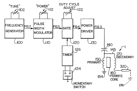
FIG. 1 is a high-level schematic functional block
diagram showing the major functional blocks of a
-5d-
i ~ ~.~., . . il n n s i . , E
CA 02152821 2004-12-08
preferred corona discharge apparatus according to the
present invention.
FIG. 2 illustrates the frequency-adjustable
(normally 500 kHz) waveform output by base frequency
generator 100.
FIG. 3 illustrates the pulse-width modulated
waveform output by pulse width modulator 110 in response
to the waveform of FIG. 2.
FIG. 4 illustrates the envelope of a waveform that
is output by gate element 120, the envelope being "on"
about half the time.
-5e-
WO 94/15391 PCT/US93/12398
21528~~-
FIG. 5 illustrates the waveform output by power driver
element 130 to the high-Q coil circuit.
FIG. 6 is a side view, partially cut away, showing a
preferred embodiment of the corona discharge apparatus
.5 according to a preferred embodiment of the present invention.
FIG. 7 is a top sectional view showing a preferred
embodiment of the coil assembly, along line 7-7 of FIG. 6.
FIG. 8 is a side sectional view of the coil assembly
according to a preferred embodiment of the present invention.
FIG. 9 is a block diagram schematically illustrating
structure of a preferred embodiment of the corona discharge
apparatus.
FIG. 10 illustrates the arrangement of FIGS. 10A, lOB,
and lOC. FIGS. 10A, lOB, and lOC (which may also be referred
to herein as ''FIG. 10", for brevity) collectively comprise a
detailed circuit level diagram of the embodiment shown
functionally in FIG. 1 and schematically in FIG. 9.
FIG. 11 illustrates a modification to the embodiment of
Figs. lOB and lOC which allows it to be a self-tuning device.
~~,tAII;ED DESCRIPTION OF THE PREFERRED EMBODIMENTS
In describing preferred embodiments of the present
invention illustrated in the drawings, specific terminology is
employed for the sake of clarity. However, the invention is
-6-
WO 94/15391 PCT/US93/12398
not intended to be limited to the specific terminology so
selected, and it is to be understood that each specific
element includes all technical equivalents which operate in a
similar manner to accomplish a similar purpose.
~ 5 The present invention provides an apparatus and method
for generating specific signals so as to produce a corona
discharge beam and magnetic fields for therapeutic treatment
of medical conditions and veterinary testing. More
particularly, the invention is useful in the treatment of pain
l0 and inflammation.
Briefly, a preferred embodiment of the present invention
functions by employing a base frequency generator 100 which
generates a 500 kHz square waveform. The generator 100 is
connected to a pulse width modulator 110 for modulating the
15 widths of the pulses of the base frequency wave. The
modulator 110 is connected to a gate arrangement 120 which
switches the modulated base frequency wave on and off
repetitively in 660 Hz cycles in accordance with a duty cycle
adjustment means and in accordance with a user's momentary
20 trigger switch 124 and a timing circuit 126 responsive to the
trigger switch. Next, the gated, modulated base frequency
wave enters a power driver element 130. The power driver
element 130 provides power to a high-Q coil assembly 1, which
WO 94/15391 ~ ~ ~ ~ ~ '~ PCT/LTS93/12398
coil assembly in turn provides high voltage to a corona
discharge pin 320.
The power driver 130 switches at 500 kHz and provides
signals in the range of about 150 to 400 volts (depending on
whether 120 VAC or 240 VAC input line. power is used). Then,
the 150-400 volt signal is stepped up to a range of
5-10 kilovolts, through use of a high-Q resonant circuit. To
form the high-Q circuit, a capacitor is connected in series
with a primary winding of a transformer in series-resonant
fashion. The secondary winding in coil assembly 1 has a 10:1
turns ratio with the primary, so that voltages of about
100 kilovolt are produced on the output of the secondary coil.
A preferred embodiment of the electronic power amplifier
according to the present invention is shown and described in
more detail with reference to FIGS. 1-10. Alterations to the
first embodiment which are needed to form an alternative
embodiment are shown in FIG. 11.
Referring now more specifically to FIGS. 1-5, a high
level functional description of the preferred embodiment of
the invention is provided.
The system includes a base frequency generator 100 which
generates a square wave at approximately 500 kHz, as
illustrated in FIG. 2. By a suitable adjustment means such as
a variable resistor 102, the exact frequency may be adjusted
-g-
WO 94/15391 PCT/US93112398
to equal the resonant frequency of a high-Q resonant circuit
associated with the output transformer of the coil assembly 1.
The base frequency generator is shown schematically,
connected to a pulse width modulator (PWM) 110. The modulator
110 modulates the pulse widths of the 500 kHz wave generated
by the base frequency generator 100, to adjust the power
output of the entire apparatus. The width of. pulses is
adjustable by a suitable adjustment means such as a variable
resistor 112. By increasing the width of the pulses, the
long-term average output power is increased; conversely, by
reducing the width of the pulses, the long-term average output
power is decreased.
The output of the pulse width modulator is shown in
FIG. 3. As shown in FIG. 3, the PWM output comprises a series
of pulses of alternating polarity, but the individual pulses
are narrower than a pure 500 kHz bipolar square wave. Between
successive alternating-polarity pulses are periods of zero
volt output. The zero volt periods are shorter when the
pulses are longer, and are longer when the pulses are shorter.
Regardless of the pulse widths, the overall waveform has a
repetition frequency of 500 kHz.
As will be described in greater detail below, the base
frequency generator 100 and pulse width modulator 110 may
collectively be implemented as a SILICON GENERAL SG3525 PWM
-g-
WO 94/15391 . PCT/US93/12398
~~.52g~~
generator or equivalent, an off-the-shelf integrated circuit
which is commonly used in switching power supplies. A
potentiometer 102 for adjusting the generator's output .
frequency, as well as a potentiometer 112 for adjusting its
output pulse width, are used directly with the SG3525.
The pulse width modulated 500 kHz wave enters a gate 120,
which gates its input (reduces to zero amplitude) at a 660 Hz
rate. The gate 120 effectively gates the 500 kHz pulse-width
modulated signal of FIG. 3 against a gating wave (preferably
l0 50~ duty cycle) gating signal of 660 Hz. The envelope of the
resultant gated waveform is shown in FIG. 4.
The frequency as well as the duty cycle of the gate's
effective gating signal is adjustable by suitable adjustment
means 122, as described in greater detail below. Within
gating element 120, the pulse-width modulated signal is gated,
either by the user removing his finger from the switch 124, by
timeout of a timer circuit 126 responsive to the user switch,
or by the "off" portion of the repetitive pulse train
determined by duty cycle adjustment means 122.
This logic, wave shaping and gating is done at the
logic power level (such as 12-13 volts), thus conserving
power.
The gated 500 kHz wave of FIG. 4 is fed into power driver
130. Power driver 130 preferably includes MOSFETs and
-10-
WO 94/15391 _ ~ 1 ~ 2 g 2 I PCT/US93/12398
fast-recovery diodes which are connected in a half bridge or
bridge topology, so as to operate as power switches. The
output of the power switches is a square wave which
corresponds to the gated, pulse-width modulated signal output
by the gate 120. The power switches switch at 500 kHz, and
provide output in the range of 150 to 400 volts depending upon
whether 120 VAC or 240 VAC is used to power the apparatus.
The 150-400 volt signal from power driver 130 is stepped
up to a range of 5 to 10 kilovolts by an LC network having the
150 volt square wave voltage input to it. In particular, the
power driver 130 is connected to a capacitor 140 which is in
series resonant arrangement with the primary winding 150 of a
transformer having a primary winding 150 and a secondary
winding 170. The high-Q properties of the resonant circuit
permit the higher-voltage (5-10 kV) sinusoidal signal to be
formed at node 145. The primary winding 150 is grounded to
power supply ground at 154.
The primary winding 150 is electrically connected to the
secondary winding 170 at node 145, and is also magnetically
coupled to it by a ferrite core 160. The primary and
secondary windings are wrapped around the ferrite core 160.
The ferrite core increases the Q of the LC circuit as seen by
power driver 130. The transformer has a 10:1 turns ratio so
-11-
WO 94/15391 PCT/US93/12398
~~~2g2~.
as to step up the primary voltage so that the secondary
winding provides a high voltage (about 100 kV) output signal.
The secondary winding i.s "air grounded°' at 174 through' a ,
discharge pin 320. The secondary winding produces the voltage
in the 30 kilovolt to 200 kilovolt range, resulting in the
desired corona discharge beam. Charge gathers at the end of
the discharge pin, which is preferably configured as a
conductive (preferably bronze) rod.
As shown in FIG. 6, an exemplary illustrated coil
assembly 1 and associated discharge pin 320, resonant circuit
node leads 145, the connection to power supply ground 154, and
the trigger switch 124 are illustrated within a housing 200.
Also illustrated are insulative support structures 310, ~ 311 in
the barrel 340 of the apparatus. The leads in node 145 to the
primary and secondary coils, the return ground 154 wire, and
the leads 224 from momentary switch 124, are all passed within
a protective sheathing 270. The leads in node 145 to the
primary and secondary coils, and the return ground 154 wire
are respectively connected to the inner conductor and outer
conductor of a co-axial cable 272 within the protective
sheathing 270.
The opposite end of the protective sheathing 270 is
connected to a cabinet (not shown) that includes other
elements of the embodiment shown in FIG. 1. In the
-12-
2.~ ~2g2~
WO 94/15391 - PCT/US93/12398
illustrated embodiment, elements 100-140 are in the cabinet,
with only the coil assembly 1 and discharge pin 320 being in
the hand-held corona discharge unit. However, it 'is
contemplated that the capacitor 140 may be included not in the
cabinet, but rather in the hand-held unit.
FIG. 7 is a top view showing a preferred embodiment of
the coil assembly, along line 7-7 of FIG. 6. FIG. 8 is a side
sectional view of the coil assembly according to the
embodiment of FIG. 6.
As shown, the coil assembly is arranged in a
substantially, radial fashion, with the substantially
cylindrical ferrite core 160 at its center. The ferrite core
160 is at ground potential. In the coil assembly generally,
voltage increases with increasing distance from the center,
with the highest voltage at the outermost portion of the
assembly.
Progressing from the center, the coil assembly is
constructed in layers, as seen most easily in FIG. 8.
1. The ferrite core 160. In the preferred embodiment, its
diameter is 0.93 inches; its length is 3.1 inches; its
preferred composition is MN80, available from MAGNETIC
CERAMICS.
-13-
WO 94/15391 PCT/US93112398
r
2152821
2. A layer of high voltage insulating tape capable of
insulating voltage in excess of 10 kV. 0.003 x 1.5
inches.
3. The primary winding 150, which is 40 turns of Litz 8/30
wire. In this embodiment, only one layer of wire is
necessary.
4. Another layer of high voltage'insulating tape.
5. A slipover tube; preferably of DELRIN~, inside diameter
1.042 inches, thickness of 0.135 inch, and length of 2.5
to inches.
6. Another layer of high voltage insulating tape.
7. The secondary winding 170, comprising 400 turns of Litz
8/30 wire. The 400 turns are arranged in 20 layers, 20
turns per layer, each layer being separated from the next
by respective layers of high voltage insulating tape.
Approximate outside diameter, 3.1 inches. The wire
itself is solid, with the conductor 0.016 inches in
diameter with the total wire diameter, including
insulation, being 0.038 inches.
8. A final layer of high voltage insulating tape.
The leads of input node 145 to the two windings, as well as
the power supply ground lead i54 to the shield, are connected
to the windings in respective layers closest to the ferrite.
-14-
WO 94/15391 , 2.~ ~ ~ g 2 ~ PCT/US93/12398
In contrast, the output 172 from the secondary, leading to the
discharge pin 320, is taken off the outermost periphery of the
secondary winding.
FIG. 9 is a block diagram schematically illustrating a
- 5 preferred embodiment of the corona discharge apparatus.
FIGS. 10A, lOB, and lOC (collectively referred to as FIG. 10
herein, for brevity) comprise a detailed circuit level diagram
of the embodiment shown functionally in FIG. 1 and
schematically in FIG. 9. FIG. 9 thus provides a closer
representation of the structure shown in the detailed circuit
diagram in FIG. 10, than does the very general functional
diagram in FIG. 1.
Referring now to FIG. 9, switch 124 is shown as a
momentary switch which shorts a positive constant voltage to
a first input of an AND gate 912. AND gate 912 provides a
gated switch signal to a 20-second ON-time pulse generator
910. The ON-time pulse generator 910 effectively functions as
a monostable multivibrator, providing non-inverting and
inverting outputs 910Q and 9loQ-, respectively.
As will be better appreciated from the discussion below,
pulse generator 910 is called an ON-time pulse generator
because, during the 20-second "window" defined by its output
pulse, the output coil of the apparatus may be on. At times
when the 20-second pulse is inactive, the coil cannot be on.
-15-
WO 94/15391 ~ PCT/US93/12398
The inverted 20-second output pulse is fed back to a
second input of the AND gate 912, to schematically illustrate
that the ON-time pulse generator does not operate as' a ,
re-triggerable pulse generator. That is, after a first rising
edge is encountered at the input of the pulse generator,
signal 910Q- blocks any further rising edges that are caused
by any repeated depressions of switch 124, from causing the
pulse generator from beginning a new 20-second,pulse.
The rising edge of inverted output signal 910Q- triggers
a second pulse generator 914, which operates as a monostable
multivibrator. Pulse generator 914 outputs a l0-second
inverted pulse 914Q- to a third input of AND gate 912. This
l0-second pulse thus extends by 10 seconds the input gating
function provided by the 20-second pulse 910Q-. It is
understood that FIG. 9 is schematic, and not literal, in
nature; accordingly, it is assumed for this discussion that
monostable multivibrator 914 has zero delay time, so that the
two blocking pulses on respective paths 910Q- and 914Q- are
deemed contiguous to form a continuous 30-second blocking
function, and do not allow a °'gap" between the two blocking
signals to re-trigger pulse generator 910.
In this manner, after switch 124 is depressed, a single
20-second period defined by a pulse at output 910Q, followed
by a 10-second period defined by a pulse at output 914Q-,
-16-
WO 94/15391 ~ ~ PCT/US93/12398
ensure that no further pulse can be generated. Accordingly,
single or repeated depressions of switch 124 during a thirty
second period result in a 20-second 910Q pulse followed by~at
least a 10-second absence of a 910Q pulse. After this
S 30-second period, new or continued depression of the switch
124 may cause another 20-second-pulse/10-second-absence.
The signal on path 910Q is provided to a first input of
an AND gate 930. A second input of AND gate 930 receives a
repetitive gating signal on path 920Q generated from a pulse
train generator 920.
Pulse train generator 920 provides a repetitive series
pulses of time duration t~ with intermediate off periods of
duration t~ therebetween. In a preferred embodiment, t~ = tuff
to provide a square wave, with t~ + t~. representing a pulse
train period of 1515.1 ~.s, corresponding to a pulse repetition
frequency period of 660 Hz. Respective t~ and tuff adjustment
means 921 and 922, such as adjustable resistors, are
illustrated. Adjustment means 921 and 922 collectively
correspond to duty cycle adjustment means 122 (FIG. 1).
In this manner, AND gate 930 gates the 660 Hz pulse train
on path 920Q against the 20-second pulse on path 910Q. During
the 20-second pulse, the output of AND gate 930 is essentially
the same as the signal on path 920Q, having a duty cycle
determined by the settings of adjustment means 921, 922 (122
-17-
WO 94/15391 PCT/US93/12398
in FIG. 1) . For example, when t~ = t~ (corresponding to a
square wave output from pulse train generator 920) , the output
of AND gate 930 is also a square wave for the duration of the
20-second period.
AND gate 930 enables a frequency-tunable pulse width
modulator (also referred to as a PWM generator) 940. When
active, PWM generator 940 generates a digital pulse train such
as that shown in FIG. 3, having a frequency determined by
frequency tuning means 102, and of pulse width determined by
width adjustment means 112.
In the preferred embodiment, the pulse frequency is about
500 kHz, finely tunable to match the resonant frequency of the
LC circuit including capacitor 140 and primary winding 150.
The pulse width is adjusted by the user as needed to provide
more output power.
When the PWM generator is enabled, opposite-polarity
pulse trains are provided on respective paths 940Q and 940Q-.
Each of these signals is represented by a waveform such as
that shown in FIG. 3, gated by a 660 Hz signal so that it is
represented by FIG. 4. Thus, it is understood that the signal
in FIG. 3 is output by the PWM generator only when the pulse
train on path 920Q is high; if the signal on path 920Q is
between pulses, AND gate 930 disables the PWM generator so
that its output goes to zero as shown in FIG. 4.
-18-
WO 94115391 , ~ PCT/US93/12398
Based on the foregoing discussion, when there is no
20-second pulse on path 910Q, the PWM generator is disabled.
Only for the duration of any 20-second pulse on path 910Q does
the PWM generator generate a 500 kHz signal, and then, only
' 5 during the acs "on'° time periods of the 660 Hz enabling pulse
train on path 920Q.
The opposite-polarity pulse trains provided on respective
paths 940Q and 940Q- are input to respective inputs of a dual
gating device 950. Dual gating device 950 includes two gates
951 and 952 which receive the signals on paths 940Q and 940Q-,
respectively. Both gates 951, 952 of-dual gating device 950
are enabled by closure of momentary switch (user push button)
124. Thus, the gated, opposite-polarity 500 kHz pulse width
modulated signals on paths 940Q and 940Q- pass through the
gates 951, 952, only at instants when the user is depressing
the momentary switch (trigger) 124. By removing his finger
from the push button 124, the user may almost instantaneously
remove power from the coils by disabling the outputs of gating
device 950.
The opposite-polarity outputs of dual gating device 950
are input to half-bridge power switch arrangement 960.
Half-bridge power switch arrangement 960 includes two
series-connected power switches 961, 962 disposed between a
higher voltage (such as 160 V) than the voltage (such as 13
-19-
WO 94/15391 PCT/US93/12398
2~~2$~~.
VDC) used by the logic in elements 910-950. When enabled,
power switches 961, 962 collectively cause generation of an
exponentially increasing sine wave in the high-Q LC circuit
140/150. The exponentially increasing sine wave is generated
in the high-Q circuit constituting capacitor 140 and primary
coil 150, through a recirculating means schematically
illustrated as element 965.
The sine wave builds exponentially to the 5 kV to 10 kV
range at the input of the primary winding 150, the exact range
being dependent on the Q of the LC circuit comprising
capacitor 140 and primary winding 150. The voltage provided
by the secondary winding 170 to the corona discharge pin 320
is determined by the turns ratio (such as 10-1) of the
secondary winding to the primary winding. In the preferred
embodiment, the voltage across the secondary, which
corresponds to the voltage from the discharge pin 320 to "air
ground" 174, is approximately 100 kV.
In summary of the operation of FIG. 9, several conditions
must concur for power to be delivered to the discharge pin
320. The user must depress the push button (momentary switch)
124 at least momentarily, to generate a 20-second pulse on
path 910Q so that AND gate 930 is "on'° during the high periods
of the pulse train on path 92oQ. Also, the user must wait at
least 30 seconds from a previous triggering of a 20-second
-20-
2.~52g2~
WO 94115391 - PCT/US93/12398
pulse on path 9lCl~, before another pulse may be generated.
(The extra 10-second waiting period included in the 30 seconds
ensures the components do not overheat, considering the high
voltages involved.) Moreover, the user must continue to
depress the momentary switch 124, in order to allow gating
arrangement 950 to pass the 500 kH2 signal to the half bridge
power driver arrangement 960 and thence to the coils.
In the preferred embodiment, adjustment means 102 and 112
are readily accessible to the user. The frequency adjustment
means 102 is aptly labelled "TUNE" near a rheostat knob or the
like. The pulse width adjustment means 112 is aptly labelled
"POWER" near another rheostat knob or the like.
However, gating pulse train duty cycle adjustment means
921, 922 (122) are preferably located inside a cabinet of the
apparatus, so that they are not readily accessible to the
user. Gating pulse train adjustment means 921, 922 (122) are
set at the time of manufacture or for maintenance purposes by
individuals who are generally more skilled than end users.
Gating pulse train adjustment means 921, 922 (122) effectively
determine a settable maximum power available to the device,
with POWER knob. 112 controlled by the user to adjust
instantaneous output power from zero to that maximum. In this
manner, gating pulse train adjustment means 921, 922 (122;
-21-
WO 94/15391 ~ ~ ~~ ~ PCT/US93/12398
ensure that, even at the maximum POWER setting on element 112 ,
no elements will be burned out by the user.
The elements in FIG. 9 may be located in a variety'of
ways. The electronics shown as elements 910 through 965 are
located in a suitable cabinet (now shown) separate from the
hand-held unit shown in FIG. 6. The capacitor 140 may be
located either in the cabinet, or in the handle of the
hand-held unit, as desired. A suitable cable joining the
cabinet to the hand-held unit must carry high voltages~if the
capacitor is located in the cabinet rather than in the
hand-held unit. However, the hand-held unit can be made
lighter and more compact by locating the capacitor in the
cabinet.
FIGS. l0A-lOC are a detailed circuit diagram of the
embodiment shown more functionally in FIG. 9. Given the
foregoing detailed description of FIG. 9, those skilled in the
art will readily appreciate the function of the detailed
disclosure in FIGS. l0A-lOC. Thus. the follnu~;r,r, .ao~..,.;.,a-;..~
is provided for convenience in facilitating an understanding
of the non-limiting embodiment described herein.
Referring now to FIG. 10A, the push button (momentary
switch) 124 is illustrated. A 2N2222 transistor is turned on
by closure of the switch, and provides an inverting function
to enable (active low enable) the dual gating arrangement 950
-22-
WO 94/15391 PCT/US93/12398
2.~~282I
(FIG. lOC). The gating arrangement 950 is implemented as an
INTERNATIONAL RECTIFIER IR 2110 driver/voltage translator.
In FIG, 10A, the first "555 timer" 910' has its pin' 6
connected to an intermediate node of an RC timing network
' S which governs the 20-second and 10-second timing pulses shown
symbolically in FIG. 9. The 44 ~,F capacitor connected to
ground is a timing capacitor, with the discharge path through
the 100 kf1 resistor governing the 10-second blocking pulse
shown symbolically on path 914Q- (FIG. 9).
Still referring to FIG, 10A, the second "555 timer" 920'
is a free-running timer generating the 660 Hz, preferably
square wave, pulse train on path 920Q (FIG. 9). Rheostats
921, 922 have exact analogs in FIG. 9.
Still referring to FIG. 10A, the AND gate 930 (FIG. 9) is
embodied by a joining of the wire outputs of the two
"555 timers" 910', 920'. This joining effectively performs a
gating function at the input to pulse width generator 940'
(FIG. lOB).
Referring to FIG. lOB, pulse width generator 940' is
preferably implemented using an SG3525A or equivalent. TUNE
and POWER rheostats 102, 112 (FIG. 9) find analogs 102', 112'
in FIG, lOB. Also illustrated in FIG, lOB is circuitry
devoted to converting 115 VAC power into 13 VDC power for use
as a DC power supply for the digital circuitry. The invention
-23-
WO 94/15391 PCT/US93/12398
provides that DC battery power may also be used to power the
device, in which case the illustrated AC-DC conversion
circuitry may be replaced by suitable DC power circuitry.
Referring to Fig 10C, the dual gate arrangement 950' is
shown, implemented as an IR2110. The dual gate arrangement
i
950' drives respective FETs (field effect transistors) 961',
962' within half bridge driver 960'. A central node between
the FETs of half-bridge driver 960' drives the high-Q circuit
15
140/150 through an arrangement of four fast diodes
collectively indicated as recirculation means 965'. The
diodes are arranged in a figure "8" configuration, with the
half-bridge's intermediate node and capacitor being connected
to the extreme ends of the "8" . Also, two fast diodes connect
in series (1) ground potential, (2) the node between the
recirculation means 965' and the capacitor 140, and (3) the
+160 V node.
Respective diodes connect the source to the drain of each
of the two FETs 961', 962', to by-pass the FETs on one
direction.
In FIG. lOC, the 160 V level is generated by a conversion
circuit receiving 115 VAC power, the details of which are not
central to the present invention. The invention provides that
DC battery power may also be used to power the device, in
-24-
WO 94!15391 ~ PCT/1TS93/12398
which case the illustrated AC-DC conversion circuitry may be
replaced by suitable circuitry for producing the 160 V level.
. As will be appreciated by those skilled in the art,
various RF filter capacitors are provided between DC power and
ground, physically close to various circuit elements, due to
the high voltage and current changes generated within the
apparatus.
During operation, the FET switches 961', 962' are turned
on and off in opposite phase, controlled by the
(approximately) 500 kHz square wave signals input to their
respective gates. In this manner, because the (approximately)
500 kHz signal is tuned precisely to the resonant frequency of
the LC circuit 140/150, the high-Q properties of the resonant
circuit allow it to support a cumulatively increasing voltage
as fed by the two FETs in successive half-cycles of the
500 kHz waveform.
The process by which the voltage in the resonant circuit
cumulatively increases may be understood as follows.
First, assume FET 961' is turned on during a first half
of a first cycle of the 500 kHz waveform, causing node 145 to
achieve a first voltage of a first polarity. Then, during the
second half of the first 500 kHz cycle, FET 962' causes the
node to achieve a second voltage twice that of the first, but
. of opposite polarity. During the first half of a second cycle
-25-
WO 94/15391 PCT/US93/12398
of the 500 kHz switching signal, the first FET 961 ~ causes the
node to achieve to a third voltage larger in magnitude than
the second voltage, but in the first polarity. During the
second half of the second cycle, the second FET 962 causes
the node to achieve a fourth voltage greater in magnitude than
the third voltage, in the second polarity.
This process continues, with the instantaneous AC peak
voltage at the node increasing to a limit determined by the Q
of the LC circuit and by the exactitude of the tuning of the
l0 frequency to the resonant frequency of the LC circuit. In
this manner, if the frequency is exactly tuned to the resonant
frequency of the LC circuit, the current and voltage
experienced by the LC circuit builds rapidly to a maximum,
displaying a waveform such as that illustrated schematically
15 in FIG. 5.
Thereafter, if any of the following conditions occur, the
process reverses:
1. The 20-second interval determined by pulse generator 910
(FIG. 9) terminates, causing AND gate 930 to disable PwM
20 generator 940.
2. A pulse in the pulse train on path 920Q goes inactive, so
that AND gate 930 disables PWM generator 940.
-26-
WO 94/15391 PCT/US93/12398
3. The user lifts his finger from the push button (momentary
switch) 124, so that dual gate arrangement 950 is
disabled.
In any of these circumstances, because either the PWM
' 5 generator 940 or the gating arrangement 950 are disabled, the
switching FETs in half-bridge driver 960 are switched off, so
that additional power is no longer provided to the resonant LC
circuit 140/150. In this event, the waveform shown in FIG. 5
decays to zero, in a time substantially determined by the Q of
l0 the LC circuit.
The invention also provides a self-tuning embodiment to
ensure that the frequency of the PWM generator is maintained
at the resonant frequency of the LC circuit 140, 150. The
self-tuning feature ensures that no manual adjustment of
15 frequency of the PWM generator 940 is necessary. This implies
that the TUNE (frequency adjustment) knob 102 is not
necessary.
Modifications of the manual tuning embodiment required to
convert it to the self-tuning embodiment are shown in FIG. 11.
20 In the self-tuning embodiment, a resistor R,.~. is inserted
between the primary winding 150 and power supply ground 154.
The resistor is effectively used to measure the current
passing through the primary winding. The node between the
-27-
WO 94/15391 ~ ~~ ~ PCT/US93/12398
resistor and the primary winding is used as a measurement
output.
As shown in the manual tuning embodiment of FIG. lOB, a
capacitor extends to ground from pins 5 and 7 of the SG3525A
PWM generator. However, to convert the FIG. lOB embodiment to
a self-tuning embodiment, the formerly grounded end of the
capacitor is connected directly to the measurement output of
the primary winding, as shown in FIG. 11.
Modifications and variations of the above-described
embodiments of the present invention are possible, as
appreciated by~those skilled in the art in light of the above
teachings. For example, the particular frequencies, signal
magnitudes, power supply magnitudes, physical dimensions,
electrical characteristics, chip implementations, and timing
characteristics of components of the illustrated embodiments
may be varied in accordance with principles known to those
skilled in the art, without departing from the scope of the
invention. It is therefore to be understood that, within the
scope of the appended claims and their equivalents, the
2o invention may be practiced otherwise than as specifically
described.
-28-