Note: Descriptions are shown in the official language in which they were submitted.
21 ~2831
T;ME-DOM~IN R~FLECTOMETER
FOR TEST-~ NG COAXIAL CABLES
This invention rela~es to tlme-domain
reflectometry and more particularly to a
time-domain reflectometry apparztus and method
for performing measu~ements on an active coaxial
network.
Backaround of the Invention
It is desirable to be able to perform
time-domain reflectometry analysis of networ~
cables, for example Ethe-net/IEEF 802.3 coaxial
cable systems, to assist in the isolation and
repair of cable faul_s and other networ~ problems.
Such determination w ll typically employ a
time-domain reflectomete_ which transmi~s a
series of pulses into the network capling and
determines the exis~ence and locztion of cabling
faults based on the reflections ~eceived in
response to the pulses anc the zmount of time
between the pulse transmission anc the received
reflection.
The time-domaln reflectomete- is 21 so useful
in measuring exact cable length which may be
des~ra~le in certain network applications.
The Internatior.21 S.andards Organlzation (ISO)
has set forth a star.dard reference model of an open
systems interconnection (OSI) to cefine the way that
participating networ~ nodes inter~ct for exchanging
information. This s~anda d provides for seven
l~yers of protocol, wherein the first layer is the
physical communicatlon layer wherein nodes of a
network are physically interconnected in some
manner. All other communications beyond the first
2l~283l
_ 2
layer are not physically connected but appear to be
to the user.
In an Ethernet system, access to the network
is provided via a carrier sense multiple access with
collision detection (CSMA/CD) standard. In such a
system, a station that wishes to transmit will first
determine whether the network is currently in use:
(carrier sense) and if the network is not in use,
the station will begin transmitting. Also the
CSMA/CD system includes collision detection wherein
if the station begins transmitting and soon there-
after detects a collision between its transmission
and the transmission of another slation, which may
not have been readily apparent prior to transmitting
because of propagation delays along the network, the
station detecting the collision will take corrective
action. In the case of an Ethernet system, this
corrective action consists of senàing a jam pattern
which the other transmitting station, which was
collided with, will recognize to indicate a
collision did occur. Retransmission is then
accomplished according to a ~'back-off algorithm"
wherein each of these two or more stations involved
in the collision will wait a random amount of time
before retransmittins. ~hus, the Ethernet system
makes use of collision between station transmissions
to efficiently regulate access to the network by
various nodes.
When performing time-domain reflectometry on
an active network, however, the pulses which are
generated by the time-domain reflectometer are of
such short duration as to go undetected by any of
the carrier sense/collision detection systems that
are designed in accordance with the international
standards for Ethernet, for example ANSI/IEEE
: 2ls~83l
_ 3
Standard 802.3. Therefore, when a collision does
occur between a time-domain reflectometry pulse and
data transmitted by a station on the network, the
transmitting station does not detect it, and bit
errors will be generated in the station's
transmitted data by the time-domain reflectometry
pulses. The error will likely be eventually
detected at a higher layer in the protocol scheme;
however, the higher in the protocol layers that
error detection occurs, the longer it takes for a
timeout to be completed based on the bit error that
was caused by the collision with the time-domain
reflectometry pulse. For example, in an Ethernet
system, level 3 and level 4 timeouts are in the
area of two to three seconds lon~. Higher level
timeouts can be up to one minute long or more.
Such delay is noticeable to network users and can
lead to user dissatisfaction with the network.
In order to avoid problems with data
corruption from time-domain reflectometry pulses,
heretofore it has been necessary to bring the
network down or inform all users to stop using the
network and observe a network silence period while
network diagnostics (particularly time-domain
reflectometry) were performed. Such solutions are
unsatisfactory as they tend to interfere with user
confidence in the network. Also, network silence
may not be observed by all users. It is desirable
to perform testing and measuremen~ on active
networks since some network problems may only arise
when the network is active and problems may be
difficult to solve if they cannot be detected and
observed by a technician as they 2re occurring.
a 21 S2831
Summary of the Invention
According to the invention, a time-domain
reflectometer is provided wherein time-domain
reflectometry is per~ormed on an operating network
without causing bit errors that would go undetected
by the media access control level protocol. A
collision detector is provided wherein any potential
collisions between the time-domain reflectometry
pulse and other dat2 frames on the network are
detected and an intentional collision is then
generated thereby causing retransmission at a lower
level in the protocol stack. The time-domain
reflectometer is connected to the network through a
crossover network and pulses are sent through an AC
path while the network is inactive, thus paralleling
the CSMA/CD operation of an Ethernet by waiting for
a clear channel be~ore transmitting. A frame
detector watches the network for an amount of time
corresponding to the propagation delay of a m~ um
length Ethernet segment plus some margin of time and
if a potential collision is observed, a collision is
enforced by placing a DC bias on the crossover
network to simulate 2 frame transmission, thereby
causing the collision detect circuits in media
access units of other stations or nodes on the
network to detect a collision.
The subject matter of the present invention
is particularly pointed out and distinctly claimed
in the concluding portion of this specification.
However, both the organization and method of
operation, together with further advantages and
objects thereof, may best be understood by
reference to the following description taken in
connection with accompanying drawings wherein like
reference characters refer to like elements.
2152831
Brief Descri~tion of the Drawings
FIG. 1 is a block diagram of an instrument
embodying a time-domaln reflectometer according to
the present invention;
FIG. 2 is a block diagram of particular
portions of the instrument of FIG. 1 when configured
to operate as a time-domain reflectometer;
FIG. 3 is schematic diagram of an implementa-
tion of a specific crossover network according to
the present invention;
FIG. 4 is a timing chart illustrating the time
relationship between the time-domain reflectometry
pulse generation and the detection of potential
collisions;
FIG. 5 is a di2srammatic representation of an
Ethernet having two coaxial cable segments and a
repeater therebetween;
FIGS. 6 and 7 together comprise~a flow chart
of a time-domain reflectometry operation according
to the present invention; and
FIG. 8 is a block diagram of a particular
implementation of window timing circuit 76 of
FIG. 2.
Detailed DescriDtion
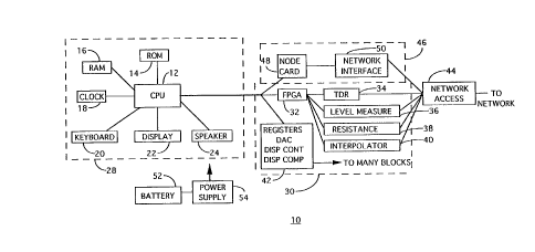
Referring now to FIG. 1, a block diagram of
an instrument embodying the present invention, the
instrument 10, a network analysis and measurement
instrument, comprises a processor 12 (CPU) which
interfaces with read only memory 14 (ROM) and
random access memory 16 (R~M), real time clock 1~,
keyboard and indicators 20, display 22 and speaker
24. Keyboard and indicators 20, display 22 and
speaker 24 suitably provide a user interface to
enable information to be reported to and received
.. , 21S2831
_ 6
from a user. The display and speaker provide
visible and audible information to the user,
while the keyboard and indicators both receive
information from the user via key strokes and
provide information to the user by, for example,
illuminating indicator LEDs to provide status or
event indication. In a particular embodiment, the
indicators may comprise separate indicators to
ascertain frame errors, collisions on an Ethernet,
polarity problems, and activity indicators to
denote the status oI the network. The indicators
may further comprise a utilization status, wherein
the percentage of network utilization may be
displayed to convey how busy the network is.
Referring further to FIG. 1, the CPU 12,
ROM 14, RAM 16, clock 18, keyboard 20, display 22
and speaker 24 together comprise the processor
sub-system 28. An analog measurement sub-system 30
is also provided and comprises a field programmable
gate array 32 (FPGA) which is configurable to
provide a series of analog measurements, including
time-domain reflectometry system 34 tTDR), level
measurement 36, DC resistance measurement 38 and
interpolator 40 which is used in conjunction with
TDR and other measurements. The analog sub-system
30 also includes block 42 which comprises
control/data registers, dlgital-to-analog converter
(DAC), display contr2st control (DISP CONT) and
display temperature compensation control (DISP COMP).
The analog sub-syste~ 30 is interconnected
to the processor via the îield programmable gate
array 32. Block 42 is also accessible via a
buffered byte bus to the processor 12.
The various analog measurement components 34,
36, 38 and 40 connec~ to network access block 44
~- 7 21 ~2 83
which comprises an active T configuration to allow
access to the network for performing tests and
operations thereon. Another sub-system comprises
the node card/network inte{face sub-system 46
wherein the node card block 48 suitably comprises
circuitry that emulates a TMS380C26 network
controller card. The network interface bloc~ 50
can include various interface functions for the
particular networks of interest, for example,
Ethernet in the specific described embodiment, or
Token-Ring or other network standard interfaces.
The network interface also connects through the
network access 44 to the network.
The instrument is powered via battery 52/power
supply 54. The battery block suitably comprises
rechargeable batteries, Lor example nickel cadmium
batteries, to enable multiple reuse cycles.
FIG. 2 is a bloc~ diagram of particular
portions of the instrument of FIG. 1 when configured
to operate as a time-domain reflectometer. Referring
to FIG. 2, the time-domain reflectometer according
to the present invention includes a pulse'generator
60 which is coupled to a driver 62 wherein the
output of the driver is supplied to a first leg of
the primary 64P of transformer 64, while the second
leg of the primary of the transformer is grounded.
A first leg of the secondary 64S or transformer 64
is attached to the center conductor of the cable
connector 66. The second leg of the secondary of
transformer 64 is connected to an end of the
parallel combination of resistor 68 and bypass
capacitor 70 wherein the opposing ends of the
resistor and capacitor are connected to ground.
Resistor 68 is suitably 50 OHMS in order to
provide the proper terminatioa impedance for a
. CA 021~2831 1998-08-24
DC path to the cable connector. Other impedances
are suitably employable in accordance with the
requirements of the particular network. Capacitor
70 provides a bypass for high frequency signals to
ground.
Also supplied is a switched current source 72
which connects with switch 71 between the second
leg of secondary 64S and ground, also in parallel
with resistor 68 and capacitor 70. Pulse generator
~ 60 provides a leading edge signal 74 which is
received by window timer 76. The output of window
timer 76 is provided to AND gate 78 as a first input
thereto. A reset signal 77 (RST) iS also supplied
to the window timer.
A detector 80 couples with the first leg of
the primary of transformer 64 and the output
thereof is supplied to a comparator 88 while a
second input of the comparator 88 is provided by
digital-to-analog converter 90 as input signal
TDR_V 92. The output of the comparator 88 is
supplied to counter/interpolator block 89, which
is in communication with the CPU 12 (FIG. 1) as
described hereinbelow. The counter/interpolator
receives the leading edge signal 74 from pulse
generator 60. Portions of counter/interpolator
block 89 correspond to interpolator 40 of FIG. 1.
Input from the network via connector 66 is
provided to a comparator 82 wherein the comparator
generates an output signal BNCNRG 84 which is
supplied to the second input of AND gate 78. The
AND gate generates an output signal 86 (collision).
The BNCNRG signal 84 is further provided to pulse
generator 60. The output signal 86 (collision) is
provided as an input to window timer 94, and the
output thereof comprises a FORCE_B signal 96. The
,; ,. , 2l~83l
~ - 9
FORCE_B signal is conveyed back to switch 71 for
governing the operation thereof as described
hereinbelow in conjunction with FIG. 2 and FIG. 3.
In operation, when time-domain reflectometry
operations are to be performed, the pulse generator
60 generates a pulse supplied to driver 62 which
is thereby coupled through the prlmary 64P of
transformer 64 to the secondary 6~S and to cable
connector 66 to be provided along the Ethernet
cable. The transformer provides 2n AC path for
transmission and reception of pulses on the
network. It should be noted that the BNCNRG signal
84, which indicates that the carrler is present on
the network, supplies the pulse generator with a
carrier detection input. If carrier is present, the
pulse generator will wait until the carrier drops
before generating the TDR pulse. Simultaneously
with the generation of the pulse, the leading edge
signal 74 is asserted which, when received by
window timer 76, begins a timing period to indicate
when to monitor for the presence of collisions.
Thus, collision signal 86 will not be asserted
unless window ti~er 76 has asserted its output to
provide the window timins output. Once the pulse
has been generated and coupled to the Ethernet
cable, any return energy will be cetected by
detector 80. The returning pulse energy is received
by comparator 88 and in accord2nce with the levels
of TDR_V 92 set by digital analog converter 90, the
comparator 88 will detect pulse returns of a
speci~ied magnitude. The magnitude thus specified
allows positive and negative pulses to be detected
of varying magnitudes which also 2110ws multiple
faults to be detected by adjustment of the level of
TDR_V along with timing as discussed hereinbelow.
CA 021~2831 1998-08-24
Once sufficient time has passed such that
any pulses sent by pulse generator 60 would have
returned and been detected by comparator 88 via
detector 80, window timer 76 asserts its output
which thus enables one leg of the AND gate 78.
Once so enabled, any energy appearing at cable
connector 66 will be detected by comparator 82.
Upon detecting such voltage on the line, comparator
82 will generate the output signal BNCNRG 84
indicating that transmissions are occurring on the
Ethernet. Thus, with the BNCNRG signal asserted
in conjunction with the window timer outpu~ signal
being asserted, both inputs to AND gate 78 are true
as will result in the output of the AND gate 78
going high indicating a collision has potentially
occurred. The window timer 76 provides several
timing windows, a first window (window 0) wherein
the output of the timer is low indicating that no
collision detection should be taking place, followed
by a second window period (window 1) which is a
specific time frame wherein the output of window
timer 76 is high, thus allowing any energy detected
by comparator 82 to result in a collision detection
that is then employed to force a collision as noted
hereinbelow. The window 1 period suitably ends
after an amount of time equal to the Ethernet slot
time (plus a small margin) has passed following the
transmission of the TDR pulse. The reason that
this time period is chosen is to account for the
possibility that the TDR instrument according the
present invention is connected to a network near
one terminal end of the network while a
transmitting station is positioned at the opposite
extreme end of the network and the transmitting
station begins its transmission just prior to the
- 11 21~2,.8~1
TDR pulse arriving at the far end of the network.
Therefore the propagation delay from one end of the
network to the other is accounted for and the
window 1 period thus ends at a time equal to twice
the end-to-end delay across an entire Ethernet
network.
According to the Ethernet specification, a
network segment can be no greater than 500 meters.
The velocity factor of a typical coaxial cable
employed with Ethernet is 0.77, so the round trip
delay time of a mA~;mum length Ethernet segment
would be as follows:
500 meters X 2
= 4.33 microseconds
~0.77 X 300,000,000 meters per sec.)
In the above formula, 500 is the~length in
meters of the network segment, which is multiplied
by 2 to account for the round trip propagation.
The speed of light is 300,000,000 meters per second
and is multiplied by the velocity factor of the
Ethernet coaxial cable (0.77) to complete the
determination of round trip propagation time of a
pulse. The 4.33 microsecond value sets the minimum
time for ending the window 0 period and beginning
the window 1 period.
An Ethernet network may comprise more than one
segment with repeaters therebetween, so the window
1 period accounts for the possible delays across
repeaters and segments for a maximum size network.
Once the window 1 period has ended, suitably 51.2
microseconds after the pulse was sent (plus a small
margin of time), a length of time equal to an
Ethernet slot time (the upper bound on the collision
~ 12 21 52831
vulnerability of a given transmission), then window
1 is finished and the window timer output again
goes low to provide a third window period (window 2).
During the window 2 period, any subsequent frame data
that appears on the Ethernet is not intentionally
collided with, since the data did not appear on the
network in a time period as would give rise to a
suspicion of collision with the TDR pulse. Prior
to subsequent TDR pulse/collision detect periods,
window timer 76 is reset by asserting RST signal 77
to ensure a new timing cycle.
If a collision is detected, then a collision is
forced on the system, since the TDR pulse generated
is of such a short duration that it would likely not
be detected as a collision by any of the stations
or nodes on the Ethernet. The present invention
therefore provides collision enforcing, enabling
low protocol level time outs to occu~ rather than
requiring that corrupted data be passed to higher
protocol levels for detection of the data errors
resulting from the collision, which would result in
long time outs noticeable to the user.
If a collision is detected in accordance with
the operation discussed hereinabove, then it is
advantageous to force a collision. In accordance
with the Ethernet specification, if a collision is
detected by a transmitting station, then
transmission must terminate and a "jam" must be
transmitted to ensure that all stations that are
participating in the collision also recognize that
it has occurred. A "jam' is suitably defined as
4 bytes of arbitrary data. In accordance with
the present invention, the transmission of arbitrary
jam data is simulated by the application of a DC
bias to the network cable via connector 66. This
13 215283l
DC bias is suitably applied by the switching on
of switch 71 whereby current source 72 is then
connected to the Ethernet cable. The current
source is such that the DC bias applied to the
Ethernet cable is approximately -1 volts which
simulates the transmission of data, given the
Ethernet signal levels of 0 and -2 volts and the
Manchester encoding of the data called for by the
Ethernet specification, wherein a transition occurs
in the middle of every bit cell. With Manchester
encoding, the first half of the bit cell contains
the complement of the bit value and the second half
of the bit cell contains the true value of the bit.
Thus, the Manchester encoded data has a 50 percent
lS duty cycle. The data rate is 10 megabits per second
which provides a 100 nanosecond length bit cell.
The DC bias applied to the network cable is
asserted for sufficient time to allow the jam to
propagate through the system, crossing any
repeaters that may be present, thereby allowing all
participating stations to recognize that a
collision has occurred. Once a sufficient time has
passed, the DC bias is removed by opening switch 71
that connects the current source to the secondary
of transformer 64S. Thus, the Ethernet back-off
algorithm, wherein stations that have participated
in a collision delay a random amount of time before
retransmitting, will be employed by stations
involved in the collision. The Ethernet back-off
algorithm for retransmission is fairly efficient
and by simulating the collision as noted
hereinabove, the TDR apparatus according to the
present invention allows quick recovery from any
collisions with the TDR pulses. When performing
TDR, multiple numbers of pulses are typically
_ 14 21 ~2831
generated in order to provide high resolution over
multiple measurements, so the quick recovery from
collisions is highly advantageous.
Referring still to FIG. 2, once the collision
signal 86 is generated, indicating that a collision
has been detected by the TDR apparatus, window
timer 94 receives the collision signal which results
in timer 94 asserting an output signal 96 (FORCE_B)
for a period of time determined in accordance with
the characteristics of the window timer. The
FORCE_B signal controls operation of switch 71 such
that when FORCE_B is asserted, switch 71 is closed,
thereby connecting current source 72 to cable
connector 66 through the secondary side of
transformer 64. When FORCE_B is deasserted, switch
71 is open and the current source is disconnected
from the cable connector. The amount of time that
FORCE_B is asserted is suitably the amount of time
dictated by the Ethernet collision protocol (i.e.,
the 8-byte time preamble transmission period plus
the jam transmission period of 4 byte time lengths),
which in a 10 megabit per second Ethernet system is
9.6 microseconds.
Referring now to FIG. 3, a schematic diagram
of a particular driven crossover network, this
implementation will be described. The driven
crossover network comprises, as discussed herein-
above, the transformer 64, the primary of which is
connected to a driver 62, and a detector 80 for
providing TDR pulses and detecting the same. The
second leg of the primary of the transformer is
connected to ground. The secondary of the
transformer is connected to the connector 66 which
suitably interfaces with the Ethernet. The second
leg of the transformer secondary is connected, as
1S 21 S2~31
noted hereinbefore, to impedance 68 which is
suitably a 50 OHM resistor in a particular
application, to provide the proper termination on
the Ethernet, so as to not result in reflections or
other problems which would appear as a result of an
improperly terminated node. Bypass capacitor 70
bypasses high frequency components to ground. The
transformer provides an AC path for signals, while
the resistor provides the proper DC termination.
Capacitor 70 removes the effect of resistor 68 for
AC path signals.
Also connected to the second leg of the
secondary of transformer 64 is the output of
switching and current source circuit 71, 72 which
corresponds to the switch 71 and current source 72
of FIG. 2. The switch and current source circuit
71, 72 comprises a resistor 100 which is connected
between the secondary of transformer~64 and the
collector of NPN transistor 102. The emitter of
transistor 102 is connected to a voltage supply,
suitably a -5 volts, while the base of transistor
102 is coupled to the collector of PNP transistor
106 by way of resistor 104. The emitter of
transistor 106 receives a +5 volt supply, while
the base of transistor 106 is supplied the
FORCE_B signal 96 (FIG. 2) via resistor 108.
In operation, when the FORCE_B signal is
asserted to force the bias to be applied to the
network for forcing a collision when a collision
has been detected, the transistor 106 is turned on
whereby transistor 102 is then turned on, thereby
applying bias to the network, as dropped by
resistor 100 to approximately -1 volt. This bias
simulates a jam signal being transmitted on the
network, and the window timer 94 (FIG. 2) assures
~ 16 21 S2 83
that the FORCE_B signal remains active for a time
to cause both transistors 106 and 102 to conduct
for a sufficient period of time to result in a
bias being applied for sufficient duration to
allow the collision to be detected across the
network, even if the signal needs to propagate
across any repeaters in the network.
In accordance with the time-domain
reflectometry instrument of the present invention,
TDR pulses are sent out across the network. The
typical pulse length is 125 nanoseconds. Such a
pulse will propagate throughout the network but
will not likely be recognized as a collision by
transmitting stations on the network. However,
even though the various transmitting stations will
not recognize this collision, the pulse is capable
of creating bit errors in the data transmitted by
a particular station. Thus, as noted hereinabove,
the bit errors will go undetected by the low-level
transmission protocol and will require that the
next level up or higher protocol determine that a
data error has occurred. The difficulty with not
detecting the bit error at the lower level
protocol is that the higher level protocol may
require 3 or 4 seconds or more before timing out
or otherwise determining that an error has
occurred. In performing the time-domain
reflectometry, a large number of pulses are sent
out in order to increase resolution and obtain
accurate measurements. Thus, the multiple pulses
will collide with frames which will result in
retransmission of the frames, but the continued
pulses of the TDR operation will potentially
collide with the resent frames and therefore the
network can slow down. Therefore, in accordance
21 S2831
_ 17
with the invention as noted hereinabove, when the
various media access units of the stations on the
network see that the DC voltage level on the
Ethernet cable (in a coaxial environment) has
dropped below the voltage that would be expected
from one station transmitting to the voltage level
as would occur when two or more stations were
transmitting, the station transmitting data which
has been corrupted by the TDR pulse will recognize
a collision has occurred. Ethernet handles
collisions very efficiently, so the present
invention advantageously makes use of this
efficient collision handling by transmitting a TDR
pulse, typically 125 nanoseconds in length, and
then waiting for an Ethernet slot time while
observing whether any frames are received during
that slot time. If a frame does occur during that
slot time, and assuming a m~x;mum allowable length
network (according to the Ethernet protocols and
standards) is present, then a bit error may have
been caused in the frame by the previously sent
pulse. Rather than do nothing and hope a bit
error did not occur, according to the present
invention, a collision is forced by employing a DC
signal applied to the cable that appears to other
stations on the network to be a transmitting
station as far as collision detection is concerned.
That DC bias propagates back to the station
transmitting the collided-with frame and that
station recognizes that its transmission has been
collided with and will back off (voluntarily delay
retransmitting in order to reduce the load on the
network) and retry the transmission according to
the Ethernet back-off protocol. The back-off
protocol is such that if a station is involved in a
- 18 21 52831
collision, a station will wait a random amount of
time before attempting to retransmit. When a
station is first involved in a collision, it will
either retransmit immediately or wait one Ethernet
slot time (which is 51.2 microseconds). After
again retrying, if the station is involved in a
collision a second time, it will next randomly
select a wait time of zero to three slot times. If
involved in still a further collision, this station
will next randomly wait any one of zero to seven
slot times. This process continues with the wait
time being randomly selected from a range of zero
to 2n-1 slot times up to n = 10.
In an Ethernet environment, the physical
layer is the lowest protocol layer and provides
a 10 megabit per second physical channel through a
coaxial cable medium. The physical layer performs
two functions that are associated with physical
channel control, data and coding, whîch include
preamble generation/removal for synchronization and
bit encoding and decoding, as well as channel
access which includes bit transmission and
reception, carrier sense which indicates traffic
on the channel and collision detection. Thus, in
accordance with the present invention, collision of
a TDR pulse with other data transmitted by other
stations on the channel is detected at the physical
layer level and is suitably responded to in the
most rapid and efficient manner available on the
Ethernet. The present invention therefore provides
the ability to perform TDR measurements on an
active network without degrading network
throughput. Once a collision is detected by the
physical layer, a data link layer is notified and
collision handling begins wherein a collision is
- 19 2152831
enforced by the transmission of a bit sequence
called a jam, thereby ensuring that the duration of
the collision is sufficient to be noticed by the
other transmitting station or stations. In the
present application, since the TDR pulse is of
insufficient duration to be noticed by other
stations on the Ethernet, the collision is enforced
by the application of the bias via the driven
crossover network discussed hereinabove with
reference to FIGS. 2 and 3. The Ethernet
specification requires that if a collision occurs
during the transmission of a preamble (a 64-bit
synchronization transmission that precedes all
frame/packets that are sent by a station), then the
preamble must be completed and then be followed by
a 4-byte jam pattern. If the preamble has already
been completed, then a 4-byte jam pattern is
sufficient. This requirement ensures that a frame
is transmitted for sufficient time to propagate the
collision throughout the network, which may include
a number of repeaters. Since the preamble is 64
bits (8 bytes) and the 4-byte jam pattern (32 bits)
is required, a corresponding 12-byte time length
bias is the minimum that should be applied by the
apparatus. Therefore, the FORCE_B signal referred
to hereinabove with reference to FIG. 3 and FIG. 2
is maintained for 12-byte times which is equal to
9.6 microseconds. This value is obtained as follows:
since the Ethernet is a 10 megabit per second system,
one bit time is 100 nanoseconds. One byte is 8 bits,
which equals 800 nanoseconds times 12 bytes equals
9600 nanoseconds which equals 9.6 microseconds.
As noted hereinabove with reference to
FIG. 2, a comparator 82 detects whether any frame
transmissions occur during the period following the
2152831
- 20
transmission/return reception of the TDR pulse
and the remainder of time in an Ethernet slot
time (an Ethernet slot time is suitably 51.2
microseconds, which is the maximum network
end-to-end round trip delay for a bit transmitted
on a segment of the network). If such energy is
detected by comparator 82, then as noted above the
BNCNRG signal 84 is asserted and if the energy is
detected during the appropriate window time, the
window timer 76 output is also asserted resulting
in a collision indication.
Referring now to FIG. 4, a timing chart
illustrating the relation of the generation of a
TDR pulse and the detection of a collision, the
timing of the window timer 76 in conjunction with
the output of a TDR pulse and the operation of the
comparator 82 (of FIG. 2) may be better understood.
In FIG. 4, the TDR pulse is represented by the
pulse generator 60 output~ line. At time T0, the
TDR pulse is generated and output through the cable
connector 66 (FIG. 2). Simultaneously with the
generation of the pulse, the signal leading edge 74
goes from low to high which, supplied to window
timer 76, instructs the timer to begin its timing
sequence. The output of window timer 76 remains
low until time T1 occurs 8.125 microseconds after
T0, which is a sufficient amount of time for the
TDR pulse to propagate round trip on a maximum
length Ethernet segment (4.33 microseconds plus a
margin of time to enable, for example, testing for
over length segments). At time T1, the output of
window timer 76 goes high whereupon the window period
begins for detecting frames on the Ethernet which
may have potentially been collided with by the TDR
pulse. This period lasts until time T2, which is
,, , 2l5283l
-- 21
suitably 51.325 microseconds after Tl, since as
noted hereinbefore, the collision, if any, will
occur within an Ethernet slot time (51.2 micro-
seconds). Once the 51.325 microsecond time period
has elapsed, then at time T2, the output of window
timer 76 goes low which prevents any traffic on the
network from being mistakenly interpreted as a
collision, since the time period during which a
collision might have occurred has now passed. The
window 2 time period continues until a reset
occurs. Upon assertion of reset signal RST 77, the
window timer is reset, whereupon subsequent TDR
pulses and measurements can occur.
FIG. 5 is a diagrammatic representation of an
Ethernet having two coaxial cable segments with a
repeater therebetween. A first cable segment 110
includes several representative stations 112
thereon, also known as nodes, wherein each station
or node is attached to the coaxial cable segment
110 by a cable tap 114. Each end of an Ethernet
segment is terminated by a 50 OHM terminator 113,
which provides a termination impedance equal to
the characteristic impedance of the network cable,
thereby eliminating reflection from the ends of the
cable. However, when performing TDR in accordance
with the instrument described herein, the TDR
apparatus 10 replaces one of the 50 OHM terminators
at one end of the segment being tested. The
location of the instrument 10 in FIG. 5 is for
illustrating placement when performing a typical
TDR operation; if not performing TDR, the TDR
apparatus can be suitably attached to the network
at any node and function as a station on the
network. Between each of the respective stations
and taps are cables 116 which connect the node or
22 21 ~2~31
station to its respective cable tap. A second
cable segment 118 is also illustrated wherein the
segment is terminated at each end by 50 OHM
terminators 113 and wherein three representative
stations 112 are present on the second segment,
connected via cables 116 and cable taps 114 to
the segment 118. Disposed between the two cable
segments 110 and 118 is a repeater 120, wherein the
repeater interconnects the two segments, a cable
tap and connector cable 114 and 116 connecting the
repeater to second segment 118 and a separate cable
116 and tap 114 connecting the repeater to the first
segment 110. A transmission of data that occurs on
either segment of 110 or 118 will be repeated and
retransmitted on the other segment by the repeater.
The operation of the TDR is such that various
reflections of different magnitudes and polarities
may be detected, to allow isolation of multiple
faults in a system. The level and polarity of the
reflection that is to be detected is set by TDR_V
signal 92 (FIG. 2) which is generated by the
digital analog converter 90 under direction of
CPU 12 (FIG. 1). Thus, comparator 88 will detect a
return pulse when the pulse exceeds the magnitude
of TDR_V. Once such a pulse is detected, the
comparator supplies a signal to counter/interpolator
circuit 89 indicating that the return pulse has been
detected. The counter and interpolator thereby
provides an accurate determination of the amount of
time elapsed between the leading edge of the pulse,
as conveyed to the counter/interpolator by leading
edge signal 74, and the receipt of the return pulse
by comparator 88. The interpolator is employed to
provide higher accuracy and more precise timing of
the return pulse. In the preferred embodiment,
_ 23 21 S283l
this interpolation is accomplished according to a
dual slope interpolation circuit, which is well
known in the art. The counter/interpolator circuit
also includes a counting and masking function which
allows various faults to be masked off whereby
faults of lesser magnitudes can be detected by
ignoring known faults of greater magnitudes. For
example, if a large magnitude fault is detected at
a time T, comparator 88 will indicate the presence
of that fault each time at T, since when TDR V is
set to a lower level for detection of smaller
magnitude faults, the large magnitude fault will
always be greater than the TDR_V level. Therefore
counter/interpolator circuit 89 in conjunction with
commands from CPU 12 will effectively ignore the
detection of the large fault by the comparator,
instead responding and timing the lesser fault.
By successively lowering the level of TDR_V, a
series of faults of various magnitudes can be
detected, whereupon subsequent determination of a
fault may be employed to provide further masking
whereby more than one fault may be ignored by the
operation of the masking function.
Referring now to FIGS. 6 and 7, which taken
together comprise a flow chart of an exemplary TDR
operation according to the present invention, this
typical TDR operation will be described. In the
illustrated embodiment, the particular operation
shown is the finding of the largest fault on the
network.
The first series of steps in the operation
comprise determining the largest positive
magnitude fault on the network. Accordingly, in
step 122, the value of TDR_V (FIG. 2) is set to a
minimum level above 0 volts. This is accomplished
_ 24 21 ~28 ~1
by the CPU instructing digital analog converter
9 0 ( F IG . 2) to generate the appropriate output
voltage to be supplied to the comparator 88 for
detecting a fault. Next, a TDR pulse is generated
(block 124) wherein pulse generator 60 of FIG. 2
is instructed by the CPU to generate a pulse of
the specified magnitude which in the preferred
embodiment is a fixed value. The pulse as
generated is passed through driver 62 via
transformer 64 to the Ethernet as connected to
cable connector 66. Once the pulse has been
generated, the pulse generator also begins operation
of counter/interpolator 89, via generation of
leading edge signal 74 (also in FIG . 2 ) . The
counter portion of block 89 will then begin timing
until a reflected pulse is detected. Thus, in step
126, a wait period is observed to allow the pulse
to propagate across the network and return. This
wait period is suitably a sufficient period of time
for the pulse to return and the delay thereof to be
calculated. In step 128, the TDR counter is read
from the counter/interpolator block 89 of FIG. 2.
The counter value is representative of the delay
from transmission of the pulse until reception of
the pulse and the actual delay is easily determined
in time units by multiplication of the counter
value by the unit of time per count.
A determination is now made whether any faults
exist, to account for the possibility that there
are no faults in the system. If there are no
faults, then the counter will have returned a
m~;m~l value indicating that no reflected pulse
was ever received. In such a case, then step 132
is performed wherein an indication is saved that no
positive magnitude faults are present and the
_ 25 21 $~83 i
positive fault delay is set to zero. The operation
then continues at off-page connector B of FIG. 7.
If in decision block 130, faults were detected,
then steps are taken to find any larger faults that
may exist, since the first fault that was located
is known to be at least as great as or greater than
the value to which TDR_V was initially set (a
minimal incremental level above 0 volts).
Accordingly, in step 134, the TDR_V iS incremented
to raise the input to comparator 88 (FIG. 2) to
allow a successively larger fault to be detected
(if present). Next, a TDR pulse is generated in
step 136 and a wait period is observed in block 138
to allow sufficient time for the pulse to return
and the delay thereof to be calculated. In step
140, the delay count is read and a determination is
again made (decision block 142) as to whether any
faults greater than or equal to the present
magnitude of TDR_V exist. If such faults do exist,
then the process loops back to continue with block
134 wherein TDR_V is again incremented. This
lncrementing, pulse, wait, read delay and check for
fault series of steps continues until such time as
a determination is made in decision block 142 that
no faults greater than or equal to the present
magnitude of TDR_V (which has been successively
incremented through the looping of the process)
exist. At such time as no such faults are
detected, the process enters block 144 wherein the
m~imum positive magnitude fault value is saved
(suitably equal to the magnitude of TDR_V on the
previous loop). In block 144, the delay to the
fault is more precisely determined. To make this
precise determination, the delay that was
associated with the largest found fault is used as
~ 26 21 52 83
a masking value for the counter/interpolator
circuit and additional TDR pulses are sent with the
value of TDR_V set to one half the value of the
largest fault that was just determined, i.e. one
half the value of TDR_V on the previous iteration.
Therefore, a TDR pulse is sent out with TDR_V set
at one half the fault magnitude from the previous
iteration, and the interpolator ignores any return
reflections except the one that occurs at around
the delay time of the fault from the previous
iteration. A reason that such a method is employed
is that a more accurate determination of the delay
time to the fault is thereby available, since the
fault time is determined to occur at the half way
point on the rising edge of the reflected pulse,
thereby providing immunity to noise occurring at
the start of the rising edge and at the end of the
rising edge of the reflected pulse. Once these
magnitude and delay values have been stored,
processing continues at off-page connector B of
FIG. 7.
Referring now to FIG. 7, off-page connector B
begins the next series of steps which will determine
the largest negative magnitude fault on the network.
Therefore, in step 146, the value of TDR_V (FIG. 2)
is set to a minimum level below zero (block 146).
As in step 122 before, this setting is accomplished
by commanding digital-to-analog converter 90
(FIG. 2) to generate an appropriate output voltage,
whereupon the output voltage is supplied to
comparator 88 for detecting a fault. Then, in step
148, a TDR pulse is generated such that pulse
generator 60 of FIG. 2 receives instructions from
the CPU to generate a pulse, suitably of a fixed
magnitude in the preferred embodiment. The pulse
;' , . 2l5283l
_ 27
passes through driver 62 via transformer 64 to the
Ethernet via cable connector 66 and at the same
time, the pulse generator starts operation of the
counter/interpolator via the leading edge signal
74. The counter in block 89 then determines the
period of time until the reflected pulse is
detected. Therefore, in block 150 a wait period is
observed to allow sufficient time for the negative
pulse to propagate through the network and be
reflected back and the delay thereof to be
calculated. Once sufficient time has passed to
allow the return pulse to be detected, the TDR
counter is read to determine the delay time to
the fault (step 152). Decision block 154 then
determines whether any faults exist. If no faults
exist, then the number of negative magnitude faults
is set to zero and the time delay to the negative
fault is set to zero, since no faults were detected
with the TDR_V comparator input set to a minimum
level below zero. Setting these two valves to zero
indicates that no negative magnitude faults exist
with a magnitude below the minimum level to which
TDR_V had been set. Processing then continues at
step 170 which is described hereinbelow.
However, in decision block 154, if faults
have been detected, then the value of TDR_V is
decremented in block 158 to lower the threshold
to attempt to determine the negative magnitude of
the negative faults that are present. A TDR pulse
is again generated in block 160 and the round trip
delay wait period is observed in step 162. Again,
in block 164, the TDR counter is read to determine
the delay between the transmission and reception of
the reflected pulse. In decision block 166 a
determination is made whether any fault exists at
_ 28 21 S2 83
this given TDR_V magnitude. If no such fault
exists, then the larsest negative magnitude fault
was equal to the magnitude of the value of TDR V on
the previous iteration through the loop 156-166
previous to the current loop. Therefore, in block
168, the negative fault magnitude is set equal to
the previous value of TDR_V and the delay to this
negative magnitude fault is then determined to a
higher precision in block 164. Much like in the
case of more precisely determining the delay to
the positive magnitude fault, the delay to the
negative fault is more precisely determined by
using the delay that was associated with the
largest found negative magnitude fault as a
masking value for the counter/interpolator
circuit. Then, additional TDR pulses are sent
with the value of TDR V set to one half the value
of the largest negative fault just determined,
i.e. one half the value of TDR_V on the previous
iteration. Therefore, a TDR pulse is sent out
with TDR_V set at one half the fault magnitude
from the previous iteration, and the interpolator
ignores any return reflections except the one
occurring at around the delay time of the fault
from the previous iteration. Again, employing such
a method enables more accurate determination of the
delay time to the fault, since the fault timing
takes place at the half way point on the falling
edge of the reflected pulse, thereby providing
immunity to noise occurring at the start of the
falling edge and at the end of the falling edge of
the reflected pulse. Processing then continues at
block 170 as discussed hereinbelow.
However, if faults still exist in block 166,
then a loop back to step 158 is performed wherein
21 ~831
29
TDR_V is again decremented to further lower the
test threshold. The looping through blocks 158-166
continues until such time as no further faults are
detected, whereupon the negative magnitude fault
will have been determined in accordance with the
values set in the previous iteration.
Referring still to FIG. 7, block 170
determines the largest fault by finding the greater
of the positive magnitude fault and the absolute
value of the negative magnitude fault. The delay
to the largest fault is then also set to be the
associated delay with the largest magnitude fault
value. The process of finding the largest fault is
then completed.
Once the largest fault has been found,
successive smaller faults can be located by masking
off the largest fault previously located and
searching for other faults. This masking is
accomplished by the counter and interpolator 89
(FIG. 2) wherein the delay time to the largest fault
is supplied to the interpolator in conjunction with
a mask signal such that the interpolator will ignore
the detection by comparator 88 of reflected energy
from the largest fault and will determine the delay
time to other faults which may be present.
By successively performing these steps,
masking off various located faults, all of the
faults which may be present in a particular cable
may be located and determined.
Referring now to FIG. 8, a block diagram of
a particular implementation of the window timing
circuit 76, the operation thereof for the detection
of collisions and generation of the collision
detection signal 86 (FIG. 2) will be further
described. The collision timing circuit receives
21S2831
_ 30
leading edge signal 74 (generated by pulse
generator 60 of FIG. 2) to one input of OR gate
172. The output of OR gate 172 is supplied as a
data input to a flip-flop 174 while the output of
the flip-flop is supplied as a second input to OR
gate 172. The flip-flop also receives a clocking
signal and a reset signal 77. The output of the
flip-flop is further provided as an input to a
first leg of AND gate 176 wherein the output of AND
gate 176 is received on the count enable line of
ripple counter 178. The ripple counter also
suitably receives a clock input and reset input 77.
In the particular embodiment, ripple counter 178
is an 8-bit ripple counter (thereby counting from
0 to 255) and the high data bit output line thereof
is supplied to an inverter 180 whereupon the
inverter output is received by ripple counter 182
as a clock input thereto. The count enable line of
ripple counter 182 is set to TRUE while reset
signal 77 is also supplied to the ripple counter
182. Ripple counter 182 is suitably a 4-bit
counter (thereby counting from 0 to 15) and the bit
zero output line thereof is supplied as a clocking
input to flip-flop 184 while the bit three output
line of counter 182 is supplied as a clock input to
flip-flop 186. Both flip-flops 184 and 186 receive
the reset signal 77 and the data input to both
flip-flops is set to TRUE. The output of flip-flop
184 comprises a window 1 signal and is supplied as
an input to one leg of three input AND gate 190
while the output of flip-flop 186 is inverted by
inverter 188 whereupon the inverted output thereof
is provided to a second input leg of AND gate 190.
The inverted output of flip-flop 186 is also
supplied as the second input to AND gate 176. The
_ 31 21 S2831
third input to three input AND gate 190 comprises
the BNCNRG signal 84 as generated by comparator 82
(FIG. 2). The output of three input AND gate 190
is supplied as input to OR gate 192 whereupon
flip-flop 194 receives the output of OR gate 192 as
its data input. Clock and reset signals are
provided also to flip-flop 194 while the output of
flip-flop 194 is fed back to comprise the second
input to OR gate 192. The output of flip-flop 194
is further provided as the collision signal 86.
The operation of the circuitry of FIG. 8 will
now be described. Prior to operation, the reset
signal 77 (RST) is asserted whereby the various
counters and flip-flops are reset such that their
output lines are respectively logic zeros. Upon
generation of a TDR pulse, the leading edge signal
74 is set to be logical one whereupon the output of
OR gate 172 becomes high. The flip-flop 174 then
has its output go high (in time with the clock
signal CLK). Since the output of the flip-flop
is fed back to OR gate 172, the data input to
flip-flop 174 remains high until a reset occurs,
since one leg of the OR gate will remain high even
after the leading edge signal 74 is removed. Once
the output of flip-flop 174 goes high, both legs of
AND gate 176 are then high, since the flip-flop
output comprises a first input to the AND gate and
the inverted output (via inverter 188) of flip-flop
186 is the second input to the AND gate, and the
flip-flop 186 has previously been reset to have a
zero output, resulting in a logical one as the
second input to AND gate 176. When the output of
AND gate 176 goes high, then the count enable line
of ripple counter 178 goes high, whereupon the
ripple counter begins its count cycle in accordance
21S2831
_ 32
with the clock signal CLK. The high bit data line
of the ripple counter is acquired as output so the
ripple counter will provide a delay by counting
from 00000000 binary to 01111111 binary before the
bit 7 data line goes high. Once the bit 7 data
line (DATA 7) goes high, the clock input to ripple
counter 182 will go low (since inverter 180 is
interposed between the two ripple counters).
Ripple counter 178 continues to count and when the
count rolls over from 11111111 to 00000000, the
bit 7 data line will go low, which will result in
the bit zero output of counter 182 going high and
accordingly the clock input to flip-flop 184
changing state whereupon the output of flip-flop
184 will go high (since the data input is tied to
a logical one). This signal as conveyed to three
input AND gate 190 comprises the window 1 enable
signal which results in the beginning of the window
timing to look for collision data (BNCNRG) on the
Ethernet. Since flip-flop 186 is initially set to
zero, the output of inverter 188 is one, so two of
the three inputs to AND gate 190 are both logical
ones. Therefore, assertion of the BNCNRG signal
84 (which occurs if comparator 82 ( FIG. 2) detects
any transmissions on the Ethernet) will result in
the output of AND gate 190 being set to logical
one.
The function of ripple counter 178 is to
divide the clock input to ripple counter 182 such
that a sufficient delay occurs before the window 1
signal is asserted and subsequently deasserted. As
ripple counter 178 continues to cycle through its
counting, every 128 counts the high bit output of
the ripple counter will change state, changing the
state of the clock to ripple counter 182. Thus,
2ls283l
_ 33
ripple counter 182 will count at a much slower
rate than counter 178 since counter 182 has a
much slower clock rate.
Once the ripple counter 182 has counted such
that its high output bit (DATA 3) becomes logical
one, the output of flip-flop 186 will go high and
as inverted by inverter 188, the third input to
AND gate 190 will go low, thereby closing the
window for observing the possibility of collision
of the TDR pulse with other data on the network.
Simultaneously with the output of flip-flop 186
going high and subsequently the output of inverter
188 going low, AND gate 176 has its output go low
since one of the inputs thereto is now low, and the
count enable line of ripple counter 178 is thereby
deasserted, resulting in counting stopping. The
flip-flop 186 through its inverter 188 in conjunc-
tion with AND gate 176 thereby halts any subsequent
state change of the output of flip-flop 184 or
flip-flop 186 such that no further energy appearing
on the network (via BNCNRG signal 84) will be
observed as colliding with the TDR pulse.
Referring again to the state where both the
output of flip-flop 184 and the inverted output of
flip-flop 186 are providing logical one inputs to
AND gate 190, if any data is detected on the
network via BNCNRG, the output of AND gate 190 will
go high. Subsequently, the output of OR gate 192
will also go high and the flip-flop 194 will have
its output become TRUE, the output remaining TRUE
since it is fed back as one input to OR gate 192
to ensure that the data input to the flip-flop 194
remains high until such time as a reset occurs.
This output of flip-flop 194 is provided as the
collision signal 86 indicating that a collision
, . 21 ~83I
between the TDR pulse and a frame of data on the
network has likely occurred. This collision signal
186 is then supplied to a second window timer 94
~FIG. 2) which controls the timing of the FORCE_B
signal assertion used to apply the collision
enforcement bias signal to the network via
transistors 106 and 102 (as discussed hereinabove
in conjunction with FIG. 3). The window timer 94
may also suitably comprise ripple counters with
appropriate timing to generate the required length
of assertion of the FORCE_B signal. As noted
hereinabove, this required length is suitably
12-byte times in an Ethernet system which in a
10 megabit per second system would comprise 9.6
microseconds.
It will be understood that the instrument in
accordance with the present invention may operate
as a node and send and receive traffic as
appropriate. However, such a state is incompatible
with the TDR mode, since when in the TDR mode, the
Ethernet cable needs to be terminated with the
proper impedance (i.e., at 50 OHMS) so as not to
generate multiple reflections as would give
inaccurate TDR readings. On the other hand, when
receiving and sending traffic, the apparatus needs
to function as a node which is a high impedance
path. In such a situation, the apparatus provides
the appropriate high impedance.
Accordingly, the present invention provides an
instrument that performs time-domain reflectometry
on an operating network without causing bit errors
as would go undetected by the media access control
level protocol. Any data frame that is transmitted
by a station on the network as may have a bit error
caused by the time-domain reflectometry pulse from
21 5~ 8
the instrument is intentionally collided with and
results in retransmission of the data frame by the
transmitting station at a much lower level in the
protocol stack. Therefore, since Ethernet is
designed to efficiently use collisions for
regulating access to the network, retransmission
occurs quickly, typically in microseconds.
While a preferred embodiment of the present
invention has been shown and described, it will be
apparent to those skilled in the art that many
changes and modifications may be made without
departing from the invention in its broader aspects.
The appended claims are therefore intended to
cover all such changes and modifications as fall
within the true spirit and scope of the invention.