Note: Descriptions are shown in the official language in which they were submitted.
BACKGROUND OF THE INVENTION
1. Field of the Invention
The invention generally relates to computer bus systems and in particular
to a method and apparatus for controlling edge rates of signals driven onto a
computer bus herein referred to as a transmission line.
2. Description of Related Art
To achieve the fastest possible bus transmission rates within modern
computer systems it is necessary to provide the fastest possible switching
rates
between logic low and logic high signals while also minimizing noise and other
factors which can affect the ability to detect signals. As far as switching
rates are
concerned, it is desirable to provide the fastest possible edge rate. By edge
rate, it
is meant the rate at which the voltage level of the bus signal is pulled up
from a
logic low voltage level to a high voltage level or vice versa. Depending upon
the
implementation, an edge rate of about 1 volt per nanosecond is desirable.
However, the faster the switching rate, the more likely ringing and other
noise
affects will result. Indeed, a sharp transition from either a high to a low or
from a
low to a high signal level will result in substantial ringing requiring a
considerable settling time. Settling time limits the ability to reliably
detect the
signal level, thereby limiting how quickly successive transitions can be
asserted
which in turn limits the data transfer rate. In many systems the fastest
overall
transmission rates are achieved with a tradeoff between fast edge rate
transitions
and overall system noise.
One technique for achieving an adequate compromise between fast edge
rates and low noise is to provide a phased output driver for driving the bus
DCM/ncg -2-
~.~8
transmission line wherein several separate output transistors are sequentially
activated, perhaps over a period of one or two nanoseconds, to achieve a
fairly
smooth transition between low and high signal states. Hence, whereas a single
output transistor maybe capable of achieving the fastest possible signal
transition, the system noise as a result of the resulting sharp transition
prevents
an overall high data transmission rate. By providing several output
transistors
which are sequentially triggered, the slope of the rising or falling edge of
the
signal is smoothed out to minimize ringing and other noise caused by a sharp
transition while still achieving a relatively fast overall signal transition.
An example of a phased output driver is illustrated in FIGURE 1. The
phased output driver of FIGURE 1 is employed within a bus system using
Gunning Transceiver Logic (GTL) wherein individual drivers pull down the
signal level on the bus. A passive pull up resistor, not illustrated in FIGURE
1, is
provided on the bus transmission line for pulling up the signal level once the
line
has been released by the phased output drive.
More specifically, FIGURE 1 illustrates a GTL phased output driver 10
having a NOR-gate pre-driver 12, a set of phasing or delay elements 14 and a
set
of output transistors 16. NOR-gate pre-driver 12 is connected to input and
enable# lines 18 and 20, respectively. A single output of NOR-gate 12 is
connected into the first of a pair of pass gate phasing elements 14. The pair
of
phasing elements are denoted by reference numerals 22 and 24. A signal output
by NOR-gate 12 is delayed first by pass gate 22, then again by pass gate 24.
The
set of output transistors includes three individual transistors, denoted 26,
28 and
30 which are connected to differing locations along the delay line of phasing
elements. In particular, a gate of transistor 26 is connected directly into
the
output of NOR-gate 12. A gate of transistor 28 is connected into the output of
DCM/ncg -3-
pass gate 22. Finally a gate of transistor 30 is connected into an output of
pass
gate 24. Drains of each of the three output transistors are connected to an
output
line 32.
With this configuration, during a pull down phase output transistor 26 is
triggered first, then, after a time delay provided by pass gate 22, transistor
28 is
triggered. Finally, after a second time delay provided by pass gate 24, output
transistor 30 is triggered. In this manner, the three output transistors are
sequentially triggered to generate an output signal which is pulled down from
a
high voltage to a low voltage at an overall rate which depends upon the
switching strengths of the individual transistors and upon the delay times of
pass
gates 22 and 24.
A low to high signal transition is achieved by sequentially deactivating the
output transistors to provide a controlled release of the output line allowing
the
external passive resistor (not shown) to pull up the line. The output
transistors
are released in the same order in which they are activated during a pull down.
FIGURE 2 illustrates an idealized high to low signal transition 34 as well
as a high to low transition 36 generated by the phased output driver of FIGURE
1. As can be seen, signal 36 provides a smooth and relatively noise free
transition
from a high voltage level to a low voltage level over a period of several
nanoseconds. FIGURE 2 also illustrates points in time 38, 40 and 42 when the
separate output transistors 26, 28 and 30, respectively, of FIGURE 1, are
triggered. As can be seen, a time delay, caused by the pass gate elements,
occurs
between the respective triggering times. The relatively fast smooth signal
transition illustrated in FIGURE 2 is achieved for a high to low signal
transition
by ensuring that transistor 30 (Figure 2) is much stronger than transistors 26
and
DCM/ncg -4-
28. Transistor 30 must be much stronger than the other two transistors because
it
is triggered last and therefore must pull down the voltage from a level which
is
already rather low. However, when the same circuit releases the output line,
thereby allowing the passive transistor to pull up the line, the resulting low
to
high transition is neither as fast nor as smooth.
FIGURE 3 illustrates an idealized low to high transition 44 and a
transition 46 generated by the phased output driver of FIGURE 1. Release times
for the three transistors are also shown in FIGURE 3. More specifically,
points
48, 50 and 52 illustrate the release times of transistors 30, 28 and 26,
respectively,
of FIGURE 1. As can be seen, the signal rises relatively slowly after the
release of
transistors 26 and 28, then jumps up erratically after transistor 30 is
released,
resulting in a substantial period of ringing which results in substantial
system
noise. The erratic noise occurs because transistor 30, which is triggered at
Hme
52, is much stronger than the other two transistors. The system noise prevents
prompt and reliable detection of the low to high transition by other elements
connected to the bus and also prevents any prompt high to low transition.
As noted, to achieve the relatively fast transition of FIGURE 2, transistor
30 must be much stronger than the other two transistors. When the transistors
are operating to pull up the output signal, transistor 30, being quite strong,
causes the abrupt and erratic signal transition illustrated in FIGURE 3. The
relative sizes of transistors could alternatively be tuned to provide for a
smooth
and quick low to high transition during the pull up phase, but such would
result
in an erratic jump in the high to low transition during the pull down phase.
In
known prior art systems, the sizes of transistors and the delays provided by
the
phasing elements are set to be equal such that adequate, but not exceptional,
DCM/ncg
performance is achieved for both low to high and high to low transitions. As
such, optimal data transmission rates are not achieved.
It would be desirable to provide an improved phased output driver for
use with busses, particularly GTL-based busses, which achieves fast edge rates
for both high to low and low to high transitions and also achieves minimal
system noise levels. It is to that end that aspects of the invention are
drawn.
DCM/ncg -6-
~~~~8
BRIEF SUMMARY OF THE INVENTION
In accordance with one aspect of the invention, an improved phased-
output driver is provided for use in connection with a computer system bus.
The
phased-output driver includes a pre-driver, a set of delay or phasing
elements,
and a set of output transistors. The pre-driver includes complementary pull up
and pull down devices, such as PMOS and NMOS devices. The output
transistors are connected through the delay elements to the PMOS transistors
in
one order but are connected to the NMOS devices of the pre-driver through the
delay elements in reverse order. 1n this manner, the output transistors are
triggered in one order to pull down an output signal and are released in
reverse
order to allow the output signal to be pulled up. The output transistors have
differing sizes. More specifically, large, medium and small transistors are
provided with the transistors arranged to be triggered in the order of small,
medium to large during the pull down phase and to be released in the reverse
order of large, medium to small during the pull up phase.
By providing output transistors of differing sizes and by triggering or
releasing the transistors in an opposite order depending upon whether a pull
down or a pull up is performed, high edge rate transitions are achieved while
also achieving minimum system noise. In particular, by triggering the largest
transistor last during a pull down phase, but by releasing the largest
transistor
first during a pull up phase, ringing problems otherwise associated with
conventional phased-output drivers are avoided.
Additional improvement may be gained by tuning both the transistor
sizes and the delay times provided by the phasing elements as well as the
number of phasing elements and drive transistors to achieve faster delay times
DCM/ncg -7-
. - ~I~~~~~
through a buffer containing the phasing elements (from input to pad) while
maintaining controlled edge rates and reduced system noise. Other
improvements may be gained by providing test inputs to the phased-output
driver for selectively activating each of the output transistors for testing
purposes.
Further improvements are gained by providing phasing elements in
which the delay time may be selected or varied. In one embodiment,
complimentary pass gates are configured with PMOS gates of each of the pass
gates connected to a logic low edge rate correction signal and with NMOS gates
connected to a logic high edge rate control signal. By selectively controlling
the
voltage level of the edge rate control signal, the impedance, and thereby the
delay time, of the pass gates is also controlled. Control of the time delay in
turn
controls the actual edge rate of the output signal.
With this configuration, the edge rate can be controlled for optimal
performance, perhaps in accordance with the physical characteristics of the
system bus including the number of loads connected thereto and including the
stub length, if any, of each individual load element. In this manner, optimal
edge
rate may be achieved in a variety of different bus systems.
The selective edge rate control of the invention is advantageously
employed with the improved phased-output driver of the invention, but may
also be employed with otherwise conventional phased-output drivers.
Moreover, although the invention is described primarily with respect to GTL
bus
drivers, principles of the invention may also be employed for CMOS bus
drivers.
Also, although the invention is described primarily with respect to PMOS and
DCM/ncg -8-
CA 02152855 1999-10-12
NMOS pull up and pull down devices, the invention is applicable to other pull
up
and pull down devices including bipolar transistors.
In one embodiment, the invention is implemented within a GTL bus
system. In general, a GTL bus can tolerate slightly faster edge rates on
falling
edges than on rising edges. For a falling edge, the GTL drive transistors are
turned on providing a low impedance path to ground. Noise due to reflections
are
thereby effectively absorbed by the driver. For the rising edge, the GTL
driver
transistors are off and the pad is in a high impedance state. Hence, noise on
the
bus is not absorbed by the driver and must be damped out elsewhere on the bus.
As a result, the edge rate for the falling edge has a higher allowable edge
rate than
that of the rising edge. This effect may be exploited in tuning the GTL output
buffer. In particular, the precise order by which the transistors are turned
on and
off and the time delays there between may be selected to tune the buffer for
optimum performance.
In each of its various embodiments, the improved phased-output drive of
the invention achieves fast delay times and controlled edge rates with low
system
noise such that overall bus transmission rates may be increased, thereby
increasing
the through-put of data, within a computer system incorporating the invention.
In one aspect, the present invention provides a phased-output driver having
a pre-driver with complementary pull-down and pull-up components, a set of
delay elements, and a set of output devices, wherein said pull-down components
are connected through said delay elements to said output devices for
sequentially
activating said output devices and said pull-up components are connected
through
said delay elements to said output devices for sequentially deactivating said
output
devices, an improvement comprising: connecting said pull-down components to
said output devices through said delay elements for activating said output
devices
-9-
CA 02152855 1999-10-12
in a first predetermined order, said output devices comprising transistors of
differing sizes and said pull-down pre-driver components being connected
through
said delay elements for activating said output transistors in order from
smallest to
largest; and connecting said pull-up components to said output devices through
said delay elements for deactivating said output devices in a second
predetermined
order, said pull-up pre-driver components are connected through said delay
elements for deactivating said output transistors in order from largest to
smallest.
In a further aspect, the present invention provides a computer system
comprising: a microprocessor; an ASIC device; a bus interconnecting said
microprocessor and said ASIC device; and wherein said microprocessor and said
ASIC device each include a phased-output driver connected through a stub line
to
said bus, each of said phased-output drivers having a pre-driver having
complimentary pull-dawn and pull-up components; a set of delay elements; and a
set of output devices; wherein said pull-down components of said pre-driver
are
interconnected through said delay elements to said output devices for
sequentially
triggering activation of said output devices in a first order; and wherein
said pull-
up components of said pre-driver are interconnected through said delay
elements
to said output devices for sequentially triggering activation of said output
devices
in a second order, differing from said first order.
In a still further aspect, the present invention provides a method for
asserting signals onto an output line connected to a passive external pull up
device, said method comprising the steps of triggering a first output device
to pull
a voltage along the output line down by a first predetermined amount;
triggering a
second output device, after a time delay period, to pull the voltage along the
output line down by a second predetermined amount; and triggering a third
output
device, after a time delay period, to pull the voltage along the output line
down by
a third predetermined amount; then releasing said third output device to allow
the
-9a-
CA 02152855 1999-10-12
voltage along the output line to be pulled up by a fourth predetermined
amount;
releasing said second output device, after a time delay period, to allow the
voltage
along the output line to be pulled by a fifth predetermined amount; and
releasing
said first output device, after a time delay period, to allow the voltage
along the
output line to be pulled up by a sixth predetermined amount.
Hence, the general objectives of the invention set forth above are achieved.
Other objects and advantages of the invention will be apparent from the
detailed
description to follow.
-9b-
~1~~8~~
BRIEF DESCRIPTION OF THE DRAWINGS
FIGURE 1 is a circuit schematic of a phased-output driver configured in
accordance with prior art.
FIGURE 2 graphically illustrates both theoretical and practical high to low
signal transitions.
FIGURE 3 graphically illustrates both theoretical and practical low to high
signal transitions.
FIGURE 4 illustrates a computer system incorporating phased-output
drivers configured in accordance with principles of the invention.
FIGURE 5 is a block diagram illustrating one of the phased-output drivers
of the computer system of FIGURE 4.
FIGURE 6 is a schematic diagram of a first exemplary embodiment of the
phased-output driver of FIGURE 5.
FIGURE 7 is a graphical illustration of theoretical and practical high to
low signal transitions generated by the phased-output driver of FIGURE 6.
FIGURE 8 is a graphical illustration of theoretical and practical low to
high signal transitions generated by the phased-output driver of FIGURE 6.
FIGURE 9 is a circuit schematic of a second exemplary embodiment of the
output driver of FIGURE 5, particularly illustrating a testability feature.
DCM/ncg -10-
~.~8~~
FIGURE 10 is a circuit schematic of a third exemplary implementation of
the output driver of FIGURE 5, particularly illustrating an adjustable edge
rate
control capability.
FIGURE 11 is a graphical illustration of actual low to high signal
transitions generated by the output driver of FIGURE 10 for a variety of edge
rate control input signal levels.
DCM/ncg -11-
DETAILED DESCRIPTION OF THE INVENTION
Referring to FIGURES 4 -11, exemplary embodiments of the invention
will now be described.
FIGURE 4 illustrates a computer system 100 having a system bus
transmission line 102 interconnecting a set of microprocessors 104, 106, 108
and
110, an I/O device 112, a memory device 114, and a pair of ASIC's 116 and 118.
The various system components shown connected to bus 102 are merely
exemplary of computer components and a wide variety of additional or
alternative computer components maybe employed. As one example, the
microprocessors illustrated in FIGURE 4 are Intel Architecture-based
microprocessors.
As can be seen from FIGURE 4, bus transmission line 102 interconnects
the various computer components in a daisy chain configuration. Opposing ends
of transmission line 102 are connected through resistors 120 and 122 to high
voltage sources which, for example, may be set to 1.5 volts. Each individual
computer component, such as microprocessor 104, includes a phased-output
driver 122 connected to bus transmission line 102 by a short interconnection
line
or stub 124. Output driver 122 is configured for driving signals onto
transmission line 102 for detection by each of the other computer components
connected to the bus. The overall logic employed for the bus system
illustrated
in FIGURE 4 is GTL logic wherein resistors 120 and 122 operate to passively
pull
up line 102 in the absence of any signals being asserted onto the line by
output
drivers 122.
DCM/ncg -12-
~15~8
Although a daisy chain configuration is illustrated, the computer
components could alternatively be interconnected with other bus topologies
including a single line topology, not shown, wherein each component is
connected through a considerably longer stub line to a single transmission
line
extending between the computer components. In such an embodiment, the
overall transmission line is about half of the length of the daisy chain
transmission line illustrated in FIGURE 4. However, the presence of the longer
stub lines results in generally higher system noise than can be achieved in
the
daisy chain configuration of FIGURE 4.
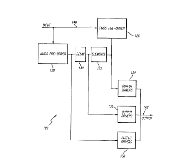
FIGURE 5 illustrates one of output drivers 122 in block diagram form.
Output driver 122 includes a PMOS pre-driver 126, an NMOS pre-driver 128,
first and second phasing or delay elements 130 and 132 and three output
devices
134, 136 and 138. The output devices may be transistors. An input signal is
received by both PMOS pre-driver 126 and NMOS pre-driver 128 along input
line 140. An output signal is generated by a combination of outputs provided
by
the three output devices along an output line 142. As noted above, although
the
invention is primarily described herein with reference to PMOS and NMOS
elements, the invention may also be applied to other pull up and pull down
devices as well.
Phasing elements 130 and 132 are both bi-directional phasing elements.
An output of NMOS pre-driver 128 is connected directly into output device 138.
The output of NMOS pre-driver 128 is also connected through phasing element
130 into output device 136. Finally, the output of NMOS pre-driver 128 is
connected through both delay elements 130 and 132 into output device 134. As
such, signals received by the output devices from NMOS pre-driver 128 are
respectively delayed.
DCM/ ncg -13-
An output of PMOS pre-driver 126 is also connected into each of the
output devices, but in a reverse order. In particular, the output of PMOS pre-
driver 126 is connected directly into output device 134, whereas output
devices
136 and 138 receive respectively delayed versions of the output signal from
PMOS driver.
As configured, the output devices are triggered in one order in response to
signals received from the PMOS pre-driver and are released in an opposite
order
in response to signals received from the NMOS driver. With a suitable choice
and number of output devices, the edge rate of a signal output along line 142
may be tuned or optimized for high pull down and pull up edge rates while also
limiting system noise.
A particular implementation of the output driver of FIGURE 6 is
illustrated in FIGURE 5. The implementation of FIGURE 6 employs PMOS
transistor elements as the PMOS driver, NMOS transistor elements as the NMOS
driver, complimentary pass gates as the phasing elements, and a set of small,
medium and large transistors as the output devices. More specifically, FIGURE
6 illustrates an output driver 222 having a pair of PMOS pre-driver
transistors
224 and 226 with gates respectively connected to an input enable# line 228 and
an input line 230. Output driver 222 also includes a pair of NMOS pre-driver
transistors 232 and 234 having gates also connected to input lines 228 and
230. A
connection line connecting the drains of NMOS transistors 232 and 234 to the
drain of PMOS transistor 226 passes through a set of pass gates 236 and 238.
Small, medium and large output transistors 240, 242 and 244 have drains
connected to an output line 246, sources connected to ground, and gates
connected to differing points or nodes along line 235.
DCM/ncg -14-
21~~~~5
As configured, PMOS transistors 224 and 226, when activated with
appropriate input signals, trigger a pull down phase which sequentially
triggers
transistors 240, 242 and 244 in that order. Hence, during pull down, the
smallest
transistor is triggered first, then after a delay period caused by pass gate
238, the
medium transistor is triggered. Finally, after a second delay period caused by
pass gate 236, the largest transistor is triggered.
During a pull up phase, NMOS transistors 232 and 234 sequentially turn
off transistors 244, 242, and 240, in that order. Hence, during pull up, the
largest
transistor is released first, then after a first delay period caused by pass
gate 236,
the medium transistor is released. Finally, after a second delay period caused
by
pass gate 238, the smallest transistor is released.
FIGURE 7 illustrates a theoretical high to low signal transition 248 and a
high to low transition to 50 generated by the output driver of FIGURE 6. As
can
be seen, a fairly prompt signal transition is achieved with minimal signal
ringing.
Within FIGURE 7, the triggering times of transistors 240, 242 and 244 are
identified by reference numerals 252, 254 and 256, respectively. By triggering
the
small and medium transistors first to initiate the pull down, and by
triggering
the largest transistor last, the overall rapid signal transition is achieved.
FIGURE 8 graphically illustrates the output signal generated by the
output driver of FIGURE 6 during a pull up phase wherein the output
transistors
are released in reverse order. In particular, FIGURE 8 illustrates a
theoretical
low to high transition 258 and an actual output signal 260 with the release
times
of transistors 240, 242 and 244 identified by reference numerals 252, 254 and
256,
respectively. As can be seen, the largest transistor is released first causing
a
significant increase in the signal level. The medium and small transistors are
DCM/ncg -15-
5
released later to complete the low to high transition. By releasing the
largest
transistor first during the pull up phase, the ringing problems illustrated in
FIGURE 3 are avoided and a controlled edge rate is achieved with minimum
buffer delay.
Now the operation of output driver 222 will be described in greater detail.
The following assumes that the enable# signal is set for enabling operation of
the
output transistor. Initially, the input line is high. The output line is also
high as
a result of the passive resistor (not shown) pulling up the transmission line.
The
input signal is switched low, causing PMOS transistor 226 to turn on thereby
activating output transistor 240 which begins to pull down the voltage applied
to
output line 246 as a result of the connection to ground. The transition of the
input line from high to low also triggers NMOS pre-driver transistor 234 to
switch OFF allowing line 235 to be pulled up by PMOS transistor 226 through
the
phasing elements.
The output signal from PMOS transistor 226 propagates through pass gate
238 where it is then applied to the gate of output transistor 242, triggering
transistor 242 to pull the voltage on output line 246 still lower. Eventually,
the
output signal from PMOS transistor 226 propagates through pass gate 236 where
it is applied to the gate of large transistor 244 causing transistor 244 to
activate
thereby pulling down the voltage along line 246 even lower.
The foregoing sequence of steps is generally reversed for the pull down
operation when the input signal is switched from low to high causing PMOS
transistor 226 to tum off and NMOS transistor 234 to turn on.
Thus, FIGURE 6 illustrates one implementation of the phased-output
driver of the invention. The implementation of FIGURE 6 includes pass gates as
DCM/ncg -16-
21~2g~5
phasing elements. However, any suitable delay element may alternatively be
employed. For example, invertors or resistors may be employed. Indeed, even a
length of transmission line may be employed with the length selected to
achieve
suitable propagation delay. Pass gates are preferred for certain applications
since
pass gates are relatively small. The implementation of FIGURE 6 also
illustrates
separate PMOS and NMOS pre-drivers which collectively form a complimentary
NOR-gate driver. Again, however, other pre-driver elements may be employed.
For example, an invertor may be employed wherein only a single PMOS
transistor and a single NMOS transistor are employed. A wide range of other
pre-drivers may be alternatively employed as well. Generally, however,
complementary pre-driver components are preferred since such allows the
PMOS components of the pre-driver to be separated from the NMOS
components of the pre-driver. Finally with respect to FIGURE 6, the output
elements are illustrated as NMOS transistors but other suitable output devices
may alternatively be employed.
With reference to FIGURE 9 a second embodiment of the invention will
now be described. FIGURE 9 illustrates a phased-output driver 322 having
many of the same elements as output driver 222 of FIGURE 6. Common
elements are illustrated with like reference numerals, incremented by 100.
Only
pertinent differences will be described.
Output driver 322 includes four output transistors 340, 342, 344 and 345 in
connection with three pass gates 336, 338 and 339. The additional pass gate
and
output transistor as compared to the driver of FIGURE 6 allows for more
precise
control of the output signal than can be achieved with the two pass gate,
three
output transistor driver of FIGURE 6.
DCM/ncg -17-
2~~28~~
Two additional pull up PMOS transistors 325 and 327 are provided along
with primary pull up transistors 324 and 326. Additional pull up transistors
325
and 327 are respectively connected to enable# and input lines 328 and 330.
Additional pull up transistors 325 and 327 are connected into the largest of
the
output transistors 345 for providing additional pull down control. However,
whereas the largest output transistor 345 is not triggered by primary PMOS
transistors 324 and 326 until after a delay time provided by pass gates 338,
336
and 339, transistor 345 is partially triggered almost immediately by secondary
pull down transistors 325 and 327. Such allows the largest transistor to begin
to
operate while the smaller transistors 340, 342 and 344 are being triggered,
such
that the largest transistor will be more effective when fully activated by the
primary PMOS transistors. Without the secondary PMOS transistors, the delay
of the turn on of output transistor 345 may be excessive, causing lower edge
rates
than desired, and increased delay through the buffer. Although not shown,
additional secondary transistors may be provided for providing pre-triggering
of
output transistors 342 and 344, although for many applications such is not
necessary.
Output driver 322 also includes test circuitry for selectively activating each
of the output transistors such that their proper operation can be verified
during
testing of the circuit. More specifically, a test# input line 331 is provided
which
is connected directly to the NMOS gates of pass gates 336, 338 and 339 and is
connected, through an invertor 333, to the PMOS gates of the pass gates. This
is
to be contrasted with output driver 226 of FIGURE 6 wherein the pass gates are
merely connected between high voltage and ground. Output driver 322 also
includes a set of four clocked invertors 360, 362, 364 and 368. Enable inputs
of
the clocked invertors are interconnected to the output of invertor 333 and to
the
DCM/ncg -18-
--- 2t~2'~~j
PMOS gates of pass gates 336, 338 and 339. Enable # inputs of invertors 360 -
368
are connected to test# input line 331. Inputs to invertors 360 - 368 are
connected
to separate test input lines 370, 372, 374 and 376.
In a test mode, active signals are applied along lines 330, 331 and 328 to
disable the PMOS and NMOS predrivers while also disabling the pass gates.
Thereafter, test signals are selectively input along lines 370 - 376 to
selectively
trigger the output transistors such that the operation of each output
transistor
can be verified. More specifically, to put the buffer in test mode, enable# is
pulled high, and the test# signal is pulled low. At this point, the PMOS and
NMOS pre-driver sections are disabled. Transistors 324 and 325 turn off the
PMOS section, and device 337 turns off the NMOS section. As such, the input is
a "don't care". Then, the pre-drivers and pass gates 339, 336 and 338 are
disabled,
and the tri-state inventors 360, 362, 364 and 366 are enabled. Output
transistors
340, 342, 344 and 345 are individually controlled by testl, test2, test3 and
test4
inputs respectively. In this manner, each drive transistor can be individually
tested.
During a regular operation mode, an inactive signal is applied along test
line 331 for reactivating pass gates 336, 338 and 339 and deactivating each of
the
test invertors 360 - 366. With the test mode deactivated, the circuit operates
as
described above to selectively pull down or pull up the output signal along
line
346 based upon input and enable signals received along lines 330 and 328,
respectively.
Finally with respect to FIGURE 9, output driver 322 also includes an
additional NMOS pull up transistor 337 which is connected between ground and
DCM/ncg -19-
~1~~8
pull down transistors 332 and 334. Additional NMOS transistor 337 is provided
for use in inverting the enable# signal.
Exemplary sizes of circuit components for use within output driver 322
are provided in Table I. The sizes provided in Table I are gate width/gate
length
in microns.
DEVICE SIZE
PMOS Transistor 3255.8/0.7
" 3235.8/0.7
32412.2/0.7
" 32612.2/0.7
NMOS Transistor 33232/0.7
" 33432/0.7
33732/0.7
PMOS Pass Gate Transistor3399.9/1.2
NMOS Pass Gate Transistor 6.0/1.2
339
PMOS Pass Gate Transistor3366.0/1.2
NMOS Pass Gate Transistor 4.3/1.2
336
PMOS Pass Gate Transistor3385.6/1.2
NMOS Pass Gate Transistor 5.6/1.2
338
NMOS Ou ut Transistor 34046.1/0.7
34291.7/0.7
344137.8/0.7
345182.9/0.7
Invertor 333N 1.3/0.7, P1.6/0.7
360N 2.6/0.7, P1.6/0.7
362N 2.6/0.7, P1.6/0.7
364N 2.6/0.7, P1.6/0.7
366N 2.6/0.7, P1.6/0.7
TABLE I
In an alternative embodiment of the circuitry of FIGURE 9, the test# input
signal line is eliminated and an invertor is connected between the enable#
line
and the pass gates, invertor 333 and the enable# inputs to invertors 360-366.
Transistor 334 is eliminated. In the alternative embodiment, to enter test
mode,
DCM/ncg -20-
~1~~8~
the enable# must be pulled high. Such disables the pre-drivers and pass gates
and enables the test tri-state buffers. The drive transistors are then
individually
driven by the test input. The alternative embodiment has the advantage that a
signal route, namely the test# signal line, is eliminated without loss of
functionality. As can be appreciated, the sizes of the various devices in the
alternative embodiment may differ from those of the embodiment of FIGURE 1
set forth in Table I.
Referring to FIGURE 10, a third embodiment of the invention will now be
described. FIGURE 10 illustrates a phased-output driver 442 having many
devices in common with the output drivers of FIGURES 6 and 9 with similar
devices being identified by like reference numerals incremented by 100 from
those of FIGURE 9. Only pertinent differences between the output driver of
FIGURE 10 and the output drivers of the FIGURES 6 and 9 will be described.
Output driver 422 is provided with an edge rate control circuit for
allowing the amount of delay provided by pass gates 436, 438 and 439 to be
selectively controlled thus allowing the edge rate for the pull down and pull
up
of the output signal to also be selectively controlled. More specifically, an
edge
rate control# (ERC#) input line 480 is connected to the PMOS gates of each of
pass gates 436, 438 and 439. An edge rate control (ERC) input line 42 is
connected to each of the NMOS gates of pass gates 436, 438 and 439. By
selecting
the voltage level for the ERC control input signals, by appropriate means not
shown, the impedance through pass gates 436, 438 and 439 is varied such that
the
delays generated by the pass gates are also varied. To achieve the least
amount
of delay and the fastest edge rates, the ERC and ERC# signals are set to the
rail
voltages. To achieve the greatest amount of delay and the slowest edge rates,
the
ERC and ERC# signals are set to intermediate voltages.
DCM/ncg -21-
~~~8~
By varying the delays provided by the pass gates, the triggering and
release times of the output transistors are varied, thereby changing the slope
of
the pull down and pull up of the output signal. Such allows the edge rate for
the
output signals to be tuned, perhaps in accordance with physical
characteristics of
the particular computer system employing the output drivers. For example, the
edge rate may be controlled based upon the number of loads applied to the
overall system bus line and in accordance with the stub length of stubs
between
the output drivers and main bus transmission line.
FIGURE 11 is a graph illustrating actual measured output signals as a
function of time for a pull-up for various voltage levels for the ERC and ERC#
signals. In FIGURE 11, time in nanoseconds is represented along the horizontal
axis 490 and the output signal in volts is represented along the vertical axis
492.
The pull up operation illustrated in FIGURE 11, was triggered at a point in
time
along the horizontal axis of about eight nanoseconds. Signal trace 494
illustrates
the output voltage when the ERC and ERC# signals are set to the rails. Each of
the remaining signal traces illustrates the output signal for differing values
of the
ERC and ERC# signals, with trace 496 illustrating a signal output when the ERC
and ERC# signals are set to be equal to one another at an intermediate voltage
level. As can be seen, the smoothest and fastest edge transition is achieved
by
setting the ERC and ERC# signals to the rails. However, a certain amount of
overshoot occurs, identified by reference numeral 498, before the output
signal
stabilizes at a voltage of about 1.5 volts. The overshoot may result in system
noise. By setting the ERC values to be closer to one another, the amount of
overshoot is decreased but the edge rate likewise decreases. For the slowest
edge
rates, such as illustrated by trace 496, the signal trace exhibits a step
behavior
caused by sequentially releasing the output transistors with too much delay
DCM/ncg -22-
2~.~28~~
between successive releases. The step behavior may further result in system
noise. For edge rate control in this area, it may be desirable to add more
stages.
The traces illustrated in FIGURE 11 were measured for an eight load
computer bus system with the driver operating at a load at one end of the
daisy
chain system bus transmission line and the signals being detected at a load at
an
opposing end of the signal line. Differing traces may result by detecting the
signals at different locations on the system bus or by generating the signals
from
differing output drivers. Nevertheless, FIGURE 11 generally illustrates that
the
edge rate can be selectively controlled using the output driver of FIGURE 10.
Finally with regard to FIGURE Il, it should be noted that each of the traces
in
FIGURE 11 exhibits initial perturbations prior to the triggering time of eight
nanoseconds. The initial perturbations are likely the result of ground
perturbations within the integrated circuit caused by operation of a clock
distribution tree.
Table II provides exemplary sizes for the various devices illustrated in
Figure 10.
DCM/ncg -23-
- 2~.~28~~
DEVICE SIZE
PMOS Transistor 425 5.8/0.7
" 423 5.8/0.7
" 424 12.2/0.7
" 426 12.2/0.7
NMOS Transistor 432 32/0.7
" 434 32/0.7
" 437 32/0.7
PMOS Pass Gate Transistor439 9.9/1.2
NMOS Pass Gate Transistor 6.0/1.2
439
PMOS Pass Gate Transistor436 6.0/ 1.2
NMOS Pass Gate Transistor 4.3/1.2
436
PMOS Pass Gate Transistor438 5.6/1.2
NMOS Pass Gate Transistor 5.6/1.2
438
NMOS Ou ut Transistor440 46.1 /0.7
" 442 91.7/0.7
" 444 137.8 / 0.7
;, - X51 --182.9/0.7
TABLE II
What have been described are exemplary embodiments of an improved
phased-output driver for use with a GTL-based bus system. Each of the output
drivers provides improved pull down and pull up edge rates in part by
triggering or releasing output transistors of differing sizes in opposite
order
depending upon whether a pull down or a pull up operation is performed.
Further improvement may be gained by providing for actual control of the delay
times of the delay elements by using an edge rate control circuit. It should
be
noted that the edge rate control circuit need not be employed only in
connection
with the improved output driver configuration having the above-described
opposite-order triggering. Rather, the edge rate control circuit may be
employed
within otherwise conventional phased-output drivers for varying the delay
times
therein. Likewise, the testability feature described above may also be
employed
within otherwise conventional output drivers. Finally, although each of the
DCM/ncg -24-
21'~~~~
embodiments illustrated in the figures are based on GTL technology, principles
of the invention may alternatively be employed for other switching
technologies,
such as CMOS. A CMOS implementation of a phased-output driver
incorporating aspects of the invention is attached hereto as Appendix A.
As far as GTL embodiments are concerned, as noted above, a GTL bus can
tolerate slightly faster edge rates on a falling edge than on a rising edge.
For the
falling edge, the GTL drive transistors are turned on providing a low
impedance
path to ground whereby noise due to reflections is eliminated or absorbed by
the
driver. For the rising edge, the GTL driver transistors are off and the pad is
in a
high impedance state or condition such that noise on the bus is not absorbed
by
the driver and must be damped out elsewhere. In one exemplary
implementation, the result is a higher allowable edge rate on the falling edge
of
1.0 volts/nanoseconds as compared to the allowable edge rate on the rising
edge
of 0.8 volts/nanoseconds. The GTL output driver may be tuned in a manner
which exploits the foregoing difference. For example, for a rising edge, the
drive
transistors may be turned off in the order of smallest to largest whereas for
the
falling edge the drive transistors may be turned on in an order which is not
exactly opposite that of the turn off order. For output drivers gate 0, gate
1, gate
2 and, gate 3, arranged in order of smallest to largest, the turn off order
may be
gate 1, gate 1, gate 2, gate 3, whereas the turn on order may be gate 3, gate
2, gate
0, gate 1. As can be appreciated, the exact order by which the output drivers
are
turned on and turned off may be selected to achieve other advantages or
objectives as well.
The circuitry described herein can be configured using a wide variety of
fabrication techniques, including, for example, silicon or gallium arsenide
techniques. As noted above, the output drivers may be employed in a wide
DCM/ncg -25-
range of computer, and other, devices. In one embodiment, the output drivers
are employed within microprocessors configured in accordance with Intel
processor Architecture. In other embodiments, the output drivers may be
employed within microprocessors configured in accordance with PowerPCTM
technology.
Although preferred and exemplary implementations of the invention have
been described, such are merely illustrative of the invention and should not
be
construed as limiting the scope of the invention. Rather, principles of the
invention may be exploited within a wide range of implementations for a wide
range of applications.
DCM/ncg -26-
Image