Note: Descriptions are shown in the official language in which they were submitted.
- 215296S
FIELD OF THE INVENTION
This invention relates to an expandable housing
for printed circuit boards.
BACKGROUND TO THE INVENTION
It is sometimes necessary to allow expansion of
a circuit physically retained on a printed circuit
board. Expansion allows a user to specify what optional
extensions of the circuit are desired. This form of
expansion is often used in the structure of personal
computers, for example, wherein a motherboard carries a
basic circuit, and connectors connected to an expansion
bus are used to connect to edge conductors of auxiliary
circuits. The result is a structure having a first
circuit board in one plane, and plural spaced circuit
boards parallel to each other orthogonal to the first
circuit board. In order to house this structure, a
cabinet must be used which has dimensions of height at
least as high as the plural circuit boards and width and
depth dimensions dictated by the motherboard.
While the cabinet requirements are clearly
large, there is another problem that dictates the size
of the cabinet that is required. The cabinet must be
made as large as must be required to accommodate as many
printed circuit boards as it is possible to connect to
the motherboard, and thus is fixed. If the motherboard
is end mounted relative to the plural circuit boards,
the width of the cabinet must be at least as wide as the
length of the motherboard. If the motherboard is side
mounted relative to the plural circuit boards, the width
of the cabinet must be at least as wide as the length of
the motherboard and at least as long as the longest of
the motherboard and plural circuit boards. In all cases
it is fixed to the above dimensions, even if there is
only a single circuit board plugged into the
- 21~296~
motherboard. Clearly the cabinet in many cases has
large empty wasted space.
In another case, the circuit board carries
plane mounted connectors which are to mate with plane
mounted connectors of another circuit board. Once
mated, the circuit boards are closely mounted and
parallel to each other. However this structure, while
requiring a cabinet which is smaller in overall volume
than the earlier example, still requires a cabinet which
has a volume sufficient to contain the maximum number of
circuit boards expected to be used.
In addition, the latter case presents other
problems. Firstly, closely mounted circuit boards are
difficult to cool, due to the very narrow space between
them necessitated by the typically shallow connectors
used to conserve space. Secondly, if the circuit boards
are spaced more distantly from each other, misalignment
of the connectors can occur due inaccuracies caused by
tolerances. In such cases it becomes increasingly
difficult to align the connector pins and connect the
circuit boards, particularly if the connectors are a
large distance from each other, i.e. on opposite sides
of the circuit boards.
Thirdly, the connectors of closely spaced
circuit boards become difficult to disengage, and tools
must be used to pry them apart. This can cause stresses
on the boards, since one side or the other of the
circuit board is typically subjected to a prying force,
which can cause flexing and breaking of conductive
tracks carried by the circuit board substrate.
SUMMARY OF THE INVENTION
The present invention is a housing for a
circuit board which facilitates circuit boards to be
connected into each other, yet grows with the number of
circuit boards used. There is thus substantially no
21~2~65
wasted space, as in the prior art housings as noted
above.
Further, the housings provide both support for,
and means for applying disengagement pressure evenly to
the edges of the circuit boards, thus minimizing flexing
and avoiding resulting cracking of conductive tracks
carried by the circuit boards.
The housings provide both means for aligning
the circuit boards (and thus their connectors),
facilitating easy connection of one circuit board to
another.
A removable side gate allows side connector
access to any of the circuit boards, giving flexibility
of connection to the contained circuit structure. The
structure is thus an excellent means for circuit boards
to have a series of connectors, one on a circuit board,
to connect to each other, and thus to provide an
extending backplane, whereby additional circuit boards
can plug into the structure, both extending the
backplane and extending the housing at the same time.
A novel sidewall to each housing works in
conjunction with a corresponding sidewall of an adjacent
sidewall to provide cooling vents, while protecting
against ingress of damaging objects into the vicinity of
the circuit board.
In accordance with an embodiment of the
invention, an electronic circuit board enclosure is
comprised of a planar member having dimensions at least
equal to dimensions of the circuit board, first pillars
fixed to at least one side of the planar member and
extending orthogonally to the planar member above the
planar member, apparatus for aligning and fixing bottoms
of second pillars of another circuit board enclosure to
tops of the first pillars, apparatus for fastening a
first circuit board to and above the planar member, and
- 215296~
locating apparatus for precisely locating the fastening
position of the circuit board to the planar member
relative to the first pillars, whereby the position of
the first circuit board can be located precisely
relative to another circuit board fastened to said
another circuit board enclosure.
In accordance with another embodiment, an
electronic circuit board enclosure assembly is comprised
of plural frame structures including apparatus for
retaining the frame structure together in a parallel
abutting relationship, a coplanar wall of each of the
frame structure having a generally U-shaped crossection,
the plane of each inner leg of each U-shape being
approximately orthogonal to the plane of a corresponding
frame structure and having a height sufficient that an
upper edge therefor abuts a lower edge of an adjacent
inner leg of an adjacent frame structure, the outer leg
of each U-shape being angled outwardly from a top of a
corresponding inner leg, whereby a bottom edge of an
outer leg of a frame structure is spaced from a top edge
of an outer leg of an adjacent frame structure, and the
inner leg of the frame structure being perforated so as
to allow air to pass therethrough and into ambient air
via spacing between the bottom edge of the outer leg and
a top edge of an outer leg of an adjacent frame
structure.
BRIEF INTRODUCTION TO THE DRAWINGS
A better understanding of the invention will be
obtained by reading the description of the invention
below, with reference to the following drawings, in
which:
Figure 1 is a section of a pair of housings in
accordance with an embodiment of the invention,
21~2965
Figures lA and lB are sectional views of part
of a housing showing alternate circuit board locating
structures,
Figure 2 is an upper isometric view of a
housing with a circuit board not in place, in accordance
with an embodiment of the invention,
Figure 2A is a crossection of several frame
walls, when several sections of housing are fixed
together,
Figure 3 is a lower isometric view of a housing
in accordance with an embodiment of the invention,
Figure 3A is an enlarged detail parts of a pair
of pillars, illustrating a key structure,
Figure 3B is an isometric view of an enlarged
detail of a pillar,
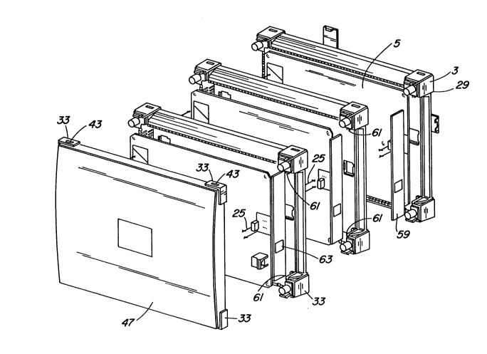
Figure 4 is an exploded isometric view of
several housing in accordance with an embodiment of the
invention, and
Figure 5 is an isometric view of the entire
structure as assembled.
DETAILED DESCRIPTION OF THE INVENTION
With reference to Figures 1, 2, 3 and 4, a
planar member 1 is fixed to pillars 3. The planar
member contains fastening members for a printed circuit
board 5, which fastening members can be standoffs 7 into
which screws 9 passing through holes in the circuit
board 5 pass. The standoffs are plastic molded together
with the planar member 1 and the pillars 3.
Typically the screw holes in the circuit board
are oversized slightly to allow the threads of the
screws to pass through without biting into the circuit
board, which could damage it. Due to the holes being
oversize, the sequence of screw tightening and the
thread rotation position when the screws are tightened,
it is possible for the precise position of one circuit
-- 21a296S
board to be different relative to the pillars than
another.
In order to position the circuit board
precisely, at least a pair of locator pins 11 is used
(only two are needed), which pass through corresponding
holes contained in the circuit board. The locator pins
11 are molded together with the planar member.
Since the locator pins can be molded at precise
locations relative to the pillars 3, and the holes in
the circuit board can be located precisely as a datum
points, the position of the circuit board relative to
the pillars 3 can be controlled with high precision.
It should be noted that other means for
locating the circuit board can be used, which use
similar principles. For example, as shown in Figure lA,
instead of a hole in the circuit board, an alignment
bracket 13 fixed to the circuit board can be used. The
locator pin 11 can pass into and be contained by a hole
15 in the alignment bracket 13.
Alternatively, as shown in Figure lB, instead
of the locator pin being molded with the planar member,
a locator pin 17 retained by the circuit board 5 can
extend into a precisely positioned hole 19 in the planar
member.
The planar member contains a slot 21, and the
circuit board retains a connector having a socket 23 and
a plug 25 at a lateral position corresponding to the
slot 21. As may be seen, a typical plug has long
standoff conductors 27, which allows the connectors of
spaced circuit boards to connect to each other. Of
course the plug and socket can be interchanged. However
it may be seen that if adjacent circuit boards are not
aligned properly, there could be sufficient misalignment
of the pins of the connectors, and it would be difficult
- ` 2152965
to connect them. The present invention provides good
precision of alignment.
The pillars preferably are comprised of holes
29 within one end thereof, and pins 31 extending from
another end thereof. The pins and holes are dimensioned
so that the holes can contain the pins with a snug fit.
A preferred form of the holes and pins can be
seen from an enlarged detail of a pillar shown in figure
3A, in conjunction with Figures 2 and 3. Since Figure 3
is an underside of the structure, the pillars shown
therein are seen from the bottom view, while the detail
of the pillar in Figure 3A is seen from the top side.
Figure 2 is a top view of the structure (with the
circuit board removed for clarity), showing the pillar
from the same side as Figure 3A
In this embodiment, the pin 31 is contained
within a shell 33, while the hole 29 is contained within
a cylindrical protrusion 35. The bottom 37 of the shell
33 abuts a shoulder 39 of the pillar when the pillar
holes 29 contain the pillar pins 31.
The pin 31 can be formed with a key 30, which
fits into slot 32. Use of this structure in one corner
can ensure that the housing sections will not be
inserted incorrectly. Use of the structure in two
opposite corners or in three or four corners can ensure
that a user could not insert three corners of the
housing structure and then try to force the fourth
corner, breaking the key.
It is also preferred that pillars should
include latching structures, for latching one housing to
the next. As shown in Figure 3A, the latching structure
is preferably comprised of a hook 41, which engages with
a slot 43 that passes through a wall of a shell 33. The
hook should be made resilient. This can be effected by
molding slots into the edges of the wall of the shell 33
21a296S
from the hook end. This provides a long hook arm, which
can flex due to the flexibility of its plastic material.
Assembly of the structure so far described may
be seen in Figure 1 and in the exploded view of Figure
4. Alignment holes in the circuit boards for each
housing section are aligned with locator pins 11, and
the circuit boards are placed against standoffs 7. The
circuit boards are fastened to standoffs 7 by screws 9.
At this point the circuit boards are precisely
positioned relative to the pillars 3.
The pillars of each section are then mated,
with the pins 31 of the pillars of one section passing
into the holes 29 of the adjacent pillars of the next
section. As the pillars are pushed together, the hooks
41 extend into the interiors of adjacent shells, and
resiliently bend, latching into slots 43. The pillars
are thereby latched together.
As the pillars are pushed together, the
connectors of adjacent circuit boards also mate. Due to
the precision of location of the circuit boards, there
is substantially no misalignment, and the connectors can
mate even if widely laterally spaced on the circuit
boards.
It is also preferred that covers 47 should be
used to enclose the entire structure. The top cover
should have the shell portions 33 of the pillars already
described at positions corresponding to the pillars 3 of
the housing section to which it is to mate. The shell
portions should contain slots 43, into which the hook 41
can latch in order to retain it securely in place. A
bottom cover (not shown), should similarly have the post
portions of pillars 3, in order to mate with the pillars
of the housing section on the other side of the
structure, and thus be retained in place.
- 21 S2965
Figure 5 illustrates an assembled multiple
section housing structure. It may be seen that the
pillars of each section are mated with, and are latched
to the pillars of a succeeding section, and the end face
of the structure is protected by cover 47. The circuit
boards are connected together. If the circuit board
connectors form a backplane for the circuitry, the
structure forms both an extending backplane (extended
only as far as is needed by the circuit boards), and at
the same time, an extending cabinet. Both the cabinet
and the backplane are of size restricted to the actual
circuit boards used, which results in a highly efficient
structure.
In accordance with another embodiment, a frame
49 is provided around at least three sides of the planar
member. Figures 2 and 2A. The frame shown in these
figures pass around only three sides, for the reason to
be described below. The frame is molded with the planar
member 1 and the sides of the opposite pillars 3.
The frame is preferably formed of a U-shaped
member 51, as may be seen in Figure 2B. The U-shaped
member is comprised of an inner leg 53 connected to an
outer leg 55. The inner leg 53 contains slots 54 or
some other form of perforations, while the outer leg 55
has no perforations. The inner leg has a width which
corresponds to the height of the pillars 3, so that when
plural housing sections are latched together the top
edge of one inner leg abuts the bottom edge of the inner
leg of the next section. The outer leg is angled away
from its edge where it connects to the inner leg.
The result may be seen in Figure 2B and Figure
5. Cooling air can pass via slots 54 into the air
channel contained between the legs, as shown by arrow
57. Due to the angle of the outer leg relative to the
bottom of the outer leg of the housing section
- 21S296~
immediately above, the air can pass into the ambient (or
can pass from the ambient via slots 54) into the region
of the circuit boards, thereby cooling it. However, due
to the outer leg having no holes, there is a sight
barrier inhibiting a person from looking look into the
interior of the housing structure. Both this
inhibition, as well as the angle and the narrowness of
the slot resulting between outer legs 55 of adjacent
housing sections, inhibits the likelihood of a person
attempting to poke a damaging object into the interior
of the housing. The slots 54 form a final barrier
against such objects.
While a structure with three walls has been
described, a structure with four walls could be used.
The fourth wall could usefully contain a hole into which
a plug could be inserted to mate with a socket retained
at a corresponding position on a circuit board.
Alternatively, as shown in Figure 4, a
removable gate 59 can be used. This gate can be held in
slots 61 molded in opposite faces of the pillars 3
adjacent the fourth side.
The gate, which can be a stiff rectangular
piece of plastic or metal, can be slid with its short
edges into the slots 61. When the structure is
assembled as shown in Figure 5, the gates block access
to the circuit boards.
The utility of the gate is that it can be
changed to accommodate the requirements of any circuit
board which is used with a particular housing section.
For example, if no circuit board side mounted connectors
are to be used with one section, the gate can have no
holes. If a side mounted connector is to be used, a
gate with one or plural holes such as hole 63 can be
inserted into slots 61. In this manner, the housing
sections can be all the same and universally used for
21~2965
all circuit boards, and no special molded structures to
suit various circuit board configurations need be
fabricated.
In addition, the top and bottom cover in
conjunction with the walls both close up the entire
structure for protection, but also give the expandable
structure a pleasing and finished appearance. The
bottom cover can contain one or more keyholes to
facilitate mounting the structure on a wall.
While pillars have been described in accordance
with a preferred embodiment as being located at corners
or a rectangular shaped planar member, it will be
recognized by a person skilled in the art understanding
this invention that other locations than those described
can be used, to suit the particular design.
A person understanding this invention may now
conceive of alternative structures and embodiments or
variations of the above. All of those which fall within
the scope of the claims appended hereto are considered
to be part of the present invention.