Note: Descriptions are shown in the official language in which they were submitted.
WO 94/17617 ~ ~ PCT/SE94I00065
1
CONTROhLED ACCE88 ATM SWITCH
BACKGROUND OF THE INVENTION
r
Field of the Invention
This invention relates to Asynchronous Transfer Mode
(ATM) switches, and in particular, to the implementation of
flow control and isochrone traffic within ATM switching
systems.
Description of Related Art
Asynchronous Transfer Mode (ATM), also known as "cell
relay", is a telecommunications standards-based technology
designed to meet the demand for the public network to simul-
taneously multiplex and twitch data over a wide spectrum of
data rates. These requirements are the result of emerging
multimedia, high-speed data and imaging applications. ATM is
a statistical multiplexing and switching method which is based
on fast packet switching concepts, and is a radical departure
from the circuit switching techniques that are used by today's
digital switches. ATM provides dedicated circuits for voice,
data, and video communications by dividing the information
flow within each of these three types of traffic into in-
dividual "cells" , each cell including an address or directions
specifying the location to which the information carried
within the cell should be delivered. Direction instructions
are added to the information carried by the cell in the form
of a label, which is processed by the ATM switch as the cell
is routed through the switch.
Several factors drive the design of broad-band ATM
switching architectures:
1. The need to accommodate a wide range of traf-
fic types from voice to video to data;
2. The high speed at which the switch has to
operate (from 155 Mb/s to over 1.2 Gb/s) ; and
SUBSTITUTE SHEET
WO 94/17617 PCT/SE94/00065
2
3. The burst-like nature of data communications.
If communications networks continue to be deployed with
large switches in central locations, then a large-scale ATM
switch will be necessary. If such a switch is to serve 50, 000 '
to 100,000 customers, each operating at the SONET STS-3 rate
(155 Mb/s), then the total customer access capacity at the
switch-customer interface is about 10 terabits per second
(Tb/s) in each direction. If only one-in-ten customers use
their assigned access capacity at any one time, then the core
of this large-scale ATM switch must be capable of switching
about 1 Tb/s of traffic, which is several orders of magnitude
larger than the capacity of today's local digital switches.
Several high-performance packet switching fabrics have
been proposed in the past. These switch fabrics can be
categorized into different architectures - internal buffer,
input buffer, output buffer, shared buffer, or various
combinations of these. Internal-buffered switches include
the buffered banyan network. With the assumption of having
single-cell buffers at the intermediate stage, and a balanced
and uniform traffic pattern, the banyan switch's maximum
throughput is only about 45% of that required for large-scale
ATM switches. Input-buffered architectures include Batcher-
banyan networks with ring reservation, or a self-routing
crossbar network with parallel, centralized contention
resolution. Because of head-of-line (80L) blocking, its
maximum throughput is about 58% of that required. Certain
techniques, such as allowing two cells of each input port to
compete with others increases the maximum throughput of input-
buffered architectures to approximately 70%.
The other types of ATM switch architectures each have
their own advantages. Switches with output buffering, for
example, have been proven to give the best delay/throughput
performance in large-scale switch architectures. The shared
buffer architectures have been shown to improve memory
utilization significantly. Other switches in the prior art
SUBS'~ITUTE SHEET
WO 94/I7617 PCTISE94/00065
3
include those equipped with mixed input and output buffers,
and a Sunshine switch implemented with both internal and
output buffers. Besides point-to-point switches, several
multicast ATM switches have also been proposed.
Each type of switch architecture has its own advantages
and disadvantages. For example, the Batches-banyan network
has fewer switch elements than a crossbar network does, but
it
has more difficulty in synchronizing all signals in every
stage because interconnection wires are not identical between
stages, and the wire-length difference increases as the
network grows. Conversely, the crossbar network has more
uniform and regular inter-connections, resulting in easier
synchronization, but it has more switch elements.
All of the prior art switches, and most of the current
research in the area of ATM switching, is oriented toward
developing switchcores of greater magnitude and complexity
in
order to provide the switching capacity necessary for a large-
scale central switch operating under its maximum projected
traffic load. Networks utilizing a dozen or more ATM chips
have been designed in such switches in order to provide the
large buffers and multiple pathways necessary to ensure a
high
probability that a cell will pass through the switchcore.
There is also a great need, however, for high quality ATM
switches which are optimally designed for smaller relay nodes
within various communications networks. None of the prior
art
ATM switch architectures, large or small, solve the capacity,
throughput, and loss problems using access control, and none
are capable of providing isochronal service,
SUMMARY OF THE INVENTION
0 30 In one aspect, the present invention is an asychronous
transfer mode (ATM) switch comprising a switchcore matrix and
a plurality of switchports electronically connected to the
switchcore matrix at input and output points. The switchports
transmit and receive information cells from the switchcore
matrix. The switchcore matrix provides routing paths for the
SUBSTITUTE SHEET
WO 94/17617 PCTlSE94/00065
2~.~~~"~?
4
routing of the information cells from the input points to the
output points on the matrix through a plurality of rows,
columns, and crosspoints thereof. The switchcore has mul-
ticast and broadcast capability. The switchports provide the
interface between the ATM switch and external communications '
devices. The switchports also interface with the switchcore
matrix by means of a switchcore interface, and control access
to the switchcore matrix by means of feedback information from
the switchcore matrix crosspoints. Access to the switchcore
matrix may be controlled by one or more input buffers which
store information cells until selected routing paths in the
switchcore matrix are free. A plurality of switchcore
matrices may be link-coupled to enhance switch performance.
In another aspect, the present invention is a method for
controlling the flow of. information cells within a com
munications system. The method begins by providing selectable
routing paths for the routing of information cells from input
points to output points of a switchcore matrix having a
plurality of rows, columns, and crosspoints thereof. A
plurality of switchports are then electronically connected to
the input and output points of the switchcore matrix to
transmit information cells thereto and receive information
cells therefrom. This is followed by connecting each of the
switchports to an external information cell communications
device, and controlling access to the switchcore matrix
available to each of the information cells. The step of
controlling access to the switchcore matrix may also include
storing the information cells in one or more input buffers
located within each of the switchports until selected routing
3o paths in the switchcore matrix are free.
It is an object of the present invention to provide an ,
ATM switch with access control, which enables the quality of
the connection through the switch to be controlled from units ,
connected thereto, and eliminates the need for large buffers
in the switchcore.
SUBSTITUTE SHEET'
CA 02153172 2001-11-09
It is another object of the present invention to
provide an ATM switch which maximizes the use of available
bandwidth for data communications traffic, which is burst-
like in nature, and which greatly reduces t=he loss rate of
5 the switch. Cell loss often occurs in prior art switches
when one stage of a switch transmits an information ce_Ll
when the buffer of the receiving stage is full. When
utilizing access control, information cells are held in
input buffers, which are sized for the type of
communications to be handled, until output buffers or ports
are available. Losses are greatly reduced because they
only occur if the input buffers are overloaded, and if the
input buffers are properly sized, overloading is very rare.
It is still another object c~f the present invention to
provide an ATM switch with properties which are similavw to
a local area network ('LAN), thereby enabling the switch to
better handle future data communications demands in public
networks.
It is still another object of the present invention to
provide an ATM switch that accommodates communications
devices of differing speeds, thereby enabling new devices
and future upgrades with higher :peed capabilities to be
attached, e.g., SONET STS 12c devices, without affecting
lower speed devices which are already attached. This
objective assures upgrading of existing equipment without
the need to replace t:he entire ATM switch, provided th<~t
the switch core is upgraded at the same time to handle the
increased speed.
It is still yet another object of the present
invention to provide an ATM switch which may be modified to
CA 02153172 2001-11-09
5a
provide a predetermined delay when transmitting information
cells, thereby enabling so-called isochronal traffic.
More specifically, the present invention provides a
data transfer switch comprising a switchcor_e matrix
comprising a plurality of rows, columns, and crosspoints
thereof, providing selectable routing paths for the routing
of a stream of information cells from input. points to
output points on the matrix, means for interfacing between
external information cell communications devices and the
switchcore matrix. The interfacing means comprises a
plurality of input switchports electronically connected to
the switchcore matrix at the input points, each of the
input switchports including at least one input buffer ;end
being associated witri one of the matrix rows, a plurality
of output switchports electronically connected to the
switching matrix at the output points, each of the output
switchports being associated with one of the matrix
columns, and means for asynchronously transmitting and
receiving the stream of information cells from the
switchcore matrix. The data transfer switch further
comprises a plurality of single-cell buffers, each of the
single-cell buffers being .located at a different one of the
crosspoints of t:he switchcore matrix, means for reporting
to each of the input switchports whether each of the
single-cell crosspoint buffers on the input switchport's
associated row contains an information cell, and means for
controlling access by the information cells to the
switchcore matrix by holding the information cells in the
input buffers until one of the single-cell crosspoint
buffers is empty.
CA 02153172 2001-11-09
5b
The present invention also provides an ATM switch
comprising a switchcore matrix comprising a plurality of
rows, columns, and crosspoints thereof, providing
selectable routing paths for the routing of a stream o:f
information cells from input points to output points on the
matrix, means for interfacing between external information
cell communications devices and t:he switchcore matrix, the
interfacing means inc:l.uding a plurality of switchports,
electronically connected to the switchcore matrix at the
input and output points, for asynchronously transmitting
and receiving the stream of information cells from the
switchcore matrix each of the switchports including at
least one input buffer sel.ective7_y sized fo:r the type of
communications traffic to be transmitted through the
buffer, and means for controlling access by the information
cells to the switchcore matrix. The means for controlling
access comprises means for holding the information cells in
the input buffer until one of the routing paths is
available, and an ATM space switching protocol which
translates logic addresses from the switchports to physical
addresses in the swit=c.hcore matrix . The A'rM space
switching protocol comprises a relay address field for
identifying target swi.tchports to which each of the
information cells is addressed, a. relay po:l1 field for
identifying which of the target switchports are free, means
for comparing the relay address field and the relay poll
field to identify which of the target switchports are both
addressed and free, and means for transmitting each of the
information cells to the addressed target switchports that
are free. The transmitting means comprises means for :phase
CA 02153172 2001-11-09
5c
shifting incoming and outgoing information cells, and means
for determining the extent of the phase shift by measuring
the length of time required to process and.assemble the
relay address field and the relay poll field.
The present invention also provides a data transfer
switch comprising a plurality of switchcore matrices, each
of the matrices comprising a plurality of rows, columns,
and crosspoints thereof, providing selectable routing paths
for the routing of information cells from input points to
1~ output points on the m;~tri_r_es, and means for interfacing
between external information cell. communications devices
and the switchcore matrices. The interfacing means
comprises plurality of input switchports electronically
connected to the switchcore matrices at the input point=s,
each of the input switc-hports including at least one input
buffer and being associated with one of the rows, a
plurality of output sw:itchports electronically connected to
the switchcore matrice:~ at the output points, each of 1=he
output switchports being associated with one of the
columns, and means for asynchronously transmitting and
receiving the stream o~ information cells from the
switchcore matrices. ')?he data transfer switch further
comprises a plurality of single-cell buffers, each of t=he
single-cell buffers being located at a different one of the
2.~ crosspoints of the switchcore matrices, means for reporting
to each of the input switchports whether each of the
single-cell crosspoint buffers on. the input. switchport"s
associated row contains an information cell, and means for
controlling access by the information cell: to the
switchcore matrices by holding the .information cells in the
CA 02153172 2001-11-09
5d
input buffer until one of the single-cell c:rosspoint
buffers is empty.
The present invention also provides a method for
controlling the flow o:~ information cells within a
communications system, the method. comprising the steps of
providing selectable routing paths for the routing of t=he
information cells from input points to output points of a
switchcore matrix having a plurality of rows, columns, and
crosspoints thereof, electronically connecting a plurality
of input switchports to the input points of the switchcore
matrix, each of the input switchports including at least
one input buffer and being associated with one of the
matrix rows, electronically connecting a plurality of
output switchports to the output points of the switchco re
matrix, each of the output switchports being associated
with one of the matrix columns, and connecting each of the
switchports to an external information cell communications
device. The method further comprises asynchronously
transmitting and receiving the stream of information cells
from the switchcore matrix, mounting a plurality of single-
cell buffers, each of the single-cell buffers being mounted
at a different one of: the crosspoints of the switchcore
matrix, reporting to each of the input switchports whether
each of the single-cell crosspoint buffers on the input
switchport's associated row contains an information cell,
and controlling acce:~s. by the information cells to the
switchcore matrix by holding the information cells in the
input buffer until ones of the single-cell crosspoint
buffers is empty.
CA 02153172 2001-11-09
5e
The present. invention also provides a method for
controlling the flow of information cells within a
communications system, the method comprising the steps of
providing selectable routing paths for the routing of the
information cells from input points to output points o:f a
switchcore matrix having a pl.ural.ity of rows, columns, and
crosspoints thereof, el.ect.ronical.ly connecting a plura:Lity
of switchports to the input points of the switchcore matrix
to transmit informati.o:a cells to the switchcore matrix,,
electronically connecting a plurality of switchports to the
output points of the switchcore matrix to receive
information cells from the switchcore matrix, connecting
each of the switchports to an exter:rial information cel:1
communications device, and controlling access, by each of
the information cell's, to the switc:hcore matrix. The
access controlling step comprises holding the information
cells in at least one input buffer located within each of
the switchports connected to the input points until one of
the routing paths is available, the step of holding the
information cells comprising selectively sizing each of the
input buffers for the type of communications traffic to be
transmitted through the buffer, and translating logic
addresses from the switchports to physical addresses in the
switchcore with an asynchronous transfer mode (ATM) space
2!~ switching protocol. The step of translating logic
addresses to physical addresses comprises identifying
target switchports to which an information cell is
addressed, identifying target switchports that are free,
comparing the addressed target switchports with the free
target switchports to identify which of the addressed
CA 02153172 2001-11-09
5f
target switchports ar_e free, and transmitting the
information cell to t:he addresseca target switchports that
are free. The transmitting step comprises measuring t:he
length of time required to identify and compare the
addressed target swit:chports with the free target
switchports, and phase shifting incoming and outgoing
information cells an amount equivalent to the length of
time required tc> identify and compare the addressed target
switchports with the free target switchports.
The present invention also provides a data transfE=r
switch comprising means for providing selectable routing
paths for the routing of the information cells from input
points to output point.:; of a swit:chcore matrix having a
plurality of rows, columns, and crosspoints thereof, means
1.5 for electronically connecting a plurality of input
switchports to the input points of the swit:chcore matrix,
each of the input switchports including at least one input
buffer and being associated with one of the matrix rows,
means for electronical:Ly connecting a plurality of output
switchports to the output points of the switchcore matrix,
each of the output switchports being associated with one of
the matrix columns, and means for connecting each of the
switchports to an external information cell. communications
device. The data transfer system further comprises means
for asynchronously transmitting and receiving the stream of
information cells from the switchcore matrix, a plurality
of single-cell buffers, each of the single-cell buffers>
being mounted at a different one of the crosspoints of the
switchcore matrix, means for reporting to each of the input
switchports whether each of the single-cell crosspoint
CA 02153172 2001-11-09
5g
buffers on the input switchport's associated row contains
an information cell and means for controlling access by the
information cells to the switchcore matrix by holding the
information cells in the input buffer unti_L one of the
single-cell crosspoint buffers is empty.
The present invention also provides a data transfer
switch comprising means for providing selectable routing
paths for the routing of the information cells from input
points to output points of a swit:chcore matrix having a
plurality of rows, cc>l.umns, and crosspoints thereof, means
for electronically connecting a Lolurality of switchports to
the input points of the switchcore matrix to transmit
information cells to t:he switchcore matrix, means for
electronically connecting a plurality of switchports to the
1.5 output points of the switchcore matrix to receive
information cells from the switchcore matrix, means fo:r
connecting each of the switchports to an external
information cell communications device, and means for
controlling access, by each of the information cells, to
the switchcore matrix. The access controlling means
comprises at least one input buffer, located within each of
the switchports connected to the input points, for holding
the information cells until one of the routing paths is
available, each of the .input buffers being selectively
sized for the type of communications traffic to be
transmitted through the buffer, and means for translating
logic addresses from tile switchports to physical addresses
in the switchcore with an asynchronous transfer mode (ATM)
space switching protocol. The means for translating logic
addresses to physical addresses comprises means for
CA 02153172 2001-11-09
5h
identifying target switchports to which an information cell
is addressed, means fo:r identifying target switchports that
are free, means for comparing the addressed target
switchports with the free target switchports to identi:Ey
which of the addressed target swi.tchports are free, and
means for transmitting the information cell to the
addressed target switc:hports that: are free. The
transmitting means comprises mearus for measuring the length
of time required to i.denti.fy and compare the addressed
target switchports with the free target switchports, and
means for phase shift:i.ng incoming and outgoing information
cells an amount equivalent to the length of time required
to identify and compare the addressed target switchports
with the free target switchports.
The present invention also provides a data transfer
switch comprising a ~>witcrlcore matrix comprising a
plurality of rows, ec>lumns, and c:rosspoints thereof,
providing selectable routing paths for the routing of a
stream of information cells from input points to output
points on the matrix, the stream of information cells being
input at a first bit rate and being output at a second bit
rate, and flow control means associated with each
crosspoint of the swit.chcore matrix for transforming t:he
bit rate of the stream of information cells from the first
bit rate to the second bit rate.
BRIEF DESCRIPTION OF THE DRAWING
The invention will be better understood, and its numerous
objects and advantages will become apparent to those skilled
in the art by reference to the following drawing in which:
WO 94/17617 PCTlSE94/00065
6
FIG. 1 is a simplified block diagram of the major
components of a controlled access ATM switch of the type
employed in the system of the present invention: '
FIG. 2 is a simplified functional block diagram of the
ATM switch of FIG. 1, illustrating the data flow between '
switchports and the switchcore, and showing where input
buffers are placed in the switchports in the system of the
present invention:
FIG. 3 is a simplified functional block diagram of the
ATM switch illustrating the manner in which operation and
maintenance functions are monitored and controlled from the
switchports in the system of the present invention;
FIG. 4 is a simplified block diagram illustrating how all
communications devices connected to the controlled access ATM
switch of the present invention have access to the switchcore
via the switchports;
FIG. 5 is a simplified functional block diagram il
lustrating the logic switching and space switching functions
performed by the controlled access ATM switch of the present
invention;
FIG. 6 is a simplified functional block diagram il-
lustrating the logic and space switching functions when
several controlled access ATM switches are link-coupled in a
matrix architecture;
FIG. 7 is a simplified functional block diagram il-
lustrating the structure and relationships between the three
communications protocol levels which perform the logic and
space switching functions in the controlled access ATM switch
of the present invention.
FIG. 8 is a block diagram illustrating the physical lines
of the switchcore interface (SCI) between one switchport and
one plane of the switchcore:
FIG. 8a is a byte map of a generic cell as it is sent in
each direction over the switchcore interface (SCI);
SUBSTITUTE SHEET
WO 94/17617 PCT/SE94/00065
7
FIG. 8b is a byte map of an information (traffic) cell as
it is sent in each direction over the switchcore interface
(scI) ;
FIG. 8c is a byte map of a maintenance cell as it is sent
in each direction over the switchcore interface (SCI) ;
FIG. 8d is a byte map of an idle cell as it is sent in
each direction over the switchcore interface (SCI):
FIG. 9 is a simplified block diagram illustrating an
embodiment of the controlled access ATM switch of the present
invention in which there are an equal number of logic buffers
in the input switchport and outlets for target switchports
from the switchcore matrix;
FIG. 10 is a simplified block diagram of an,embodiment of
the controlled access ATM switch of the present invention in
which a single logic buffer is used for all switchcore outlets
to target switchports;
FIG. 11 is a simplified block diagram illustrating buffer
prioritizing and the use of variable buffer sizes in the input
side of the switchports of the controlled access ATM switch of
the present invention:
FIG. 12 is a functional diagram showing the connection of
the switchports to the switchcore and illustrating the
principle employed for the access mechanism to the switch
matrix in the controlled access ATM switch of the present
invention;
FIG. 13 is a functional diagram illustrating a minimal
solution for the positioning of buffers in the switchcore
matrix which still provides the desired functionality of the
controlled access ATM switch of the present invention;
FIG. 14 is a functional diagram illustrating the positio-
ping of buffers in the switchcore matrix when an intermediate
number of buffers are employed in the controlled access ATM
switch of the present invention;
FIG. 15 is a functional diagram illustrating the posi-
tinning of buffers in the switchcore matrix in a complete
solution in which one buffer, one cell deep, is used for each
SUBSTITUTE SHEET
WO 94/17617 PCT/SE94/00065
..
matrix cross-point in the controlled access ATM switch of the
present invention;
FIG. 16 is a top level block diagram of a switchcore '
matrix:
FIG. 17 is a block diagram of a row function unit (RFU)
of the switchcore matrix;
FIG. 18 is a block diagram of a column function unit
(CFU) within the switchcore matrix;
FIG. 19 is a high level flow chart of a software program
which controls the functions of a CFU controller within the
column function unit (CFU);
FIG. 20 is a block diagram of a cross function unit (XFU)
within the switchcore matrix:
FIG. 21 illustrates the timing relationship between the
switchport-to-switchcore cell stream and the switchcore-to
switchport cell stream within the switchcore interface (SCI)
for a specific switchport;
FIG. 22 is a perspective view of one embodiment of the
controlled access ATM switch of the present invention in which
a single-chip switchcore is mounted on a back plane to which
switchport boards are connected; and
FIG. 23 is a logical block diagram of the devices used
for speed conversion in the preferred embodiment of the
present invention.
DETAILED DESCRIPTION OF THE INVENTION
FIG. 1 is a simplified block diagram of the major
components of an controlled access ATM switch 10 of the type
employed in the implementation of the principles of the
present invention. The ATM switch of the present invention is
essentially comprised of two parts: one or more switchports ,
11 and a switchcore 12. Each switchport 11 performs the logic
switching and buffering functions of the ATM switch 10 , and is
divided into an input side 11A and an output side 11B, as
shown in FIG. 2. The switchcore 12 essentially performs only
routing functions based on a label added to each information
SUBSTITUTE SHEET
WO 94/17617 ~ '' PCTISE94/00065
9
cell, and may be implemented in a single chip. This greatly
reduces the hardware and maintenance cost of the switchcore,
and greatly increases its reliability, especially if a second
plane 13 is provided for redundancy, as shown in FIG. 1.
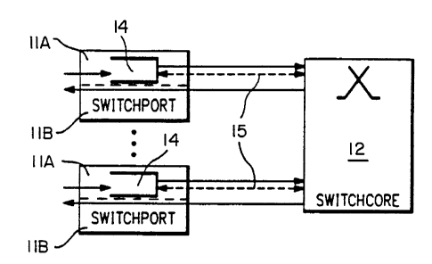
FIG. 2 is a simplified functional block diagram il-
lustrating the data flow between switchports 11 and the
switchcore 12, and showing where input buffers 14 are placed
in the switchports 11. In one embodiment, the switchcore 12
in the present invention is greatly simplified over the prior
art switches. This is in part because the input buffers 14
are moved from within the switchcore 12, where thev are
located in most coventional ATM switches, to the input side of
the switchports 11A. The switchcore 12 therefore comprises
only a switch matrix and a status register for each column in
the matrix with an appended prioritizing mask register for,
fair transmission of cells. The switchcore 12 has a buffer
depth of only one store for each path or route, and has no
processor or any other communication channel for operation and
maintenance.
The consequence of buffering in the switchport 11 is that
the bandwidth must be increased on the input side 11A of each
individual switchport connection to enable the switchport to
receive a large amount of data in a short period or to receive
data from several input sources nearly simultaneously.
However, the storage capacity of each buffer 14 can be
tailored to the individual requirements of each switchport 11,
and of the type of traffic it handles, thereby improving
overall system characteristics and cost. Each switchport 11
may be designed with a different sized input buffer 14, and
may be made either more or less complex, depending on the type
of communications service involved. For example. for conven-
tional telephone service, with a continuous, low data-rate
- flow of information through the switch, a small input buffer
14 will suffice. For data communications, the information
flow of which is more burst-like in nature, a larger input
buffer 14 is required. Thus, overall cost of the ATM switch
SUBSTITUTE SHEET
WO 94/17617 PCT/SE94/00065
10 is reduced since the design of the input buffers 14 can be
tailored to the anticipated service type, and only the
necessary buffer space provided.
In addition to the advantages of tailored individual
5 buffer distribution, the introduction of access control and
buffering in the switchport 11 provides a "guarantee" that the
cells will pass through the switchcore 12 because the switch
port 11 holds the cell in its buffer 14 while determining the
status of its assigned routes through the switchcore 12, and
10 releases the cell only when a route and a destination switch-
port is free.
The dotted line 15 in FIG. 2 represents the flow of
access monitoring and protocol control information.(PCI)
which determines when each switchport 11 can transmit the
information in its input buffer 14 through the switchcore 12.
This monitoring and control process will be discussed in
greater detail below.
The communication between the switchcore 12 and the
different switchports 11 may be asynchronous or synchronous.
The asynchronous communication is controlled by each switch
port 11 and allows one switchport to send and receive at a
high rate while another switchport sends and receives at a low
rate. The synchronous communication requires that the
switchports 11 requiring synchronization use a clock distri-
bution signal in the switchcore 12. In this case one switch-
port acts as a master, and the other switchports act as
slaves. The master switchport delivers the synchronizing
clock signal to the slave switchports.
FIG. 3 is a simplified functional block diagram i1
lustrating the manner in which operation and maintenance
functions are monitored and controlled from the switchports
11. Each switchport 11 controls and monitors the opei.-ation
and maintenance (O&M) functions on the routes in the switch
core 12 which are capable of being used by each respective
switchport 11. The dashed lines 16a in FIG. 3 indicate that
SUBSTITUTE SHEET
WO 94/17617 ~ ~ ~ ~ ~ PCT/SE94/00065
11
the O&M functions are performed on the routes through the
switchcore 12 , but not on the switchcore itsel f .
FIG. 4 is a simplified block diagram illustrating how all
communication devices 17 connected to the controlled access
ATM switch 10 have access to the switchcore 12 via the
switchports 11. The switchports 11 provide the interface
between the communication devices 17 and the switchcore 12.
The switchports 11 may, for example, when carrying standard
telephone traffic, convert the signal from standard C1 carrier
format into ATM packet format having up to 56 bytes of
information in each cell.
FIG. 5 is a simplified functional block diagram il-
lustrating the logic switching and space switching functions
performed by the controlled access ATM switch of the present
invention. The logic and space switching functions are
implemented through three protocol levels: ATM Logic Swit-
ching (ALS) 18, ATM Space Switching (ASS) 19 and physical
framing 21. ALS 18 provides the interface between the ATM
switch 10 and external network devices 17, and is performed
within the switchports 11. ALS 18 translates incoming Virtual
Channel Identifier/Virtual Path Identifier (VCI/VPI) numbers
to outgoing numbers on both the input and output sides of the
ATM switch 10. ASS 19 is a protocol which passes information
cells between switchports 11 and the switchcore 12. ASS 19 is
performed as the logic address from the switchport 11 is
translated in the switchcore 12 to a physical address for
space switching. Physical framing 21 indicates that the
transfer of cells may be aligned with a framing reference in
order to synchronize switchports 11 to each other.
Of the three protocols described, ATM Space Switching
(ASS) 19 is the protocol with the greatest significance to the
present invention. ASS 19 is a collection of functions and
procedures carried out on an ATM Space Switch level. The
functions are carried out partly in the switchport 11 and
partly in the switchcore 12. The functions enable the
' extraction of cellsync and bytesync, maintenance of the
SUBSTITUTE SHEST
WO 94/17617 PCT/SE94/00065~
12
switchcore 12, control of access to the switchcore, and
determination of the status of sent/received cells. The
functions are driven by the protocol control information (PCI) '
15 transmitted from switchport 11 to switchcore 12 (and vice
versa) and by the primitives from superior or controlling
layers.
FIG. 6 is a simplified functional block diagram il-
lustrating the logic and space switching functions when
several controlled access ATM switches 10 are link-coupled in
a matrix architecture or any other structure such as CLOS.
Providing large buffers 14 in the switchports (SWP) 11a-d
permits a high degree of concentration without impairing the
properties of the system for data communication traffic
through the switchcores (SWC) 12a-c. The divided line in the
ALS level of the inner switchports 11b and 11c illustrates
symbolically that there are two mutually facing selector
ports.
FIG. 7 is a simplified functional block diagram il
lustrating the structure and relationships between the three
communications protocol levels which perform the logic and
space switching functions in the controlled access ATM switch
10 of the present invention. An ATM-cell 24, comprising 53
bytes of information, may be stored in the ALS-PDU. When the
cell is put into the ALS-SDU 22, which comprises 56 bytes of
information, three (3) bytes are left for free use. The ALS-
SDU 22, together with the PCI 15 of 4 bytes, are then put into
the ASS-PDU 27 which comprises 60 bytes, and are then relayed
to the other ALS-entity 18 or vice versa. The functions are
performed partly in the switchport 11 and partly in the
switchcore 12. The functions are driven by the PCI 15
transmitted from switchport 11 to switchcore 12 (and vice
versa) and by primitives from superior of controlling layers.
The switchcore interface (SCI) is the interface between
the switchports 11 and the switchcore 12. Information cells,
maintenance cells and idle cells are mixed on the SCI. The
information cells are routed through the switchcore 12 while
SUBSTITUTE SHEET
WO 94/17617 ~' PCT/SE94/00065
13
the maintenance and idle cells are terminated on both sides of
the SCI.
FIG. 8 is a block diagram illustrating the physical lines
of the SCI between one switchport 11 and one plane of the
switchcore 12. The physical lines comprise a bi-directional
CLOCK ref line 28, a DCLOCK SWP-SWC line 29 from switchport 11
to switchcore 12 , a DATA SWP-SWC 1 ine 3 0 from switchport 11 to
switchcore 12, a DATA SWC-SWP line 31 from switchcore 12 to
switchport 11, and a DCLOCK SWC-SWP line 32 from switchcore 12
to switchport 11. Thus, each line except the CLOCK ref line
28 is implemented as a balanced pair.
FIG. 8a is a byte map of a generic cell 101 as it is sent
in each direction over the SCI. The cell contains 60 bytes
with bit 8 on byte ~1 transmitted first in a serial bit-stream.
Bytes 1-4 constitute an address and validation field 10.2, and.
bytes 5-60 are the payload (information) 103 carried by the
cell 101. As an option for high data rates, and in particular
when optical transmission line is used, a Line Code Bit (LCB)
104 may be inserted every 24th bit. Together with a two-step
scrambling, the LCB 104 gives good DC balance. The switchcore
12 detects the LCB 104 and uses the same technique in the
opposite direction for each individual switchport 11.
A cell type field (CTF) 105 is a two-bit coded field
which is used in both directions. The codes in the CTF 105
indicate what type of cell is being transferred. The fol
lowing codes, with their interpreted meanings are included:
Code Type of Cell Remarks
00 Idle cell RAF not valid; RPF valid.
01 Maintenance Carries maintenance command;
RAF, RPF replaced by mainte-
nance fields; see maintenance
cell format (FIG. 8c).
10 Active traffic Low prio cell; RAF, RPF valid
SUBSTITUTE SHEET
WO 94117617 ~ PCTISE94/00065
14
11 Active traffic High prior RAF, RPF valid.
A tag error check (TEC) field 106, comprising a field of
6 bits, is generated and checked on both sides of the SCI. The
TEC 106 is used for both cell synchronization and validation
of the previous 26 bits in the cell.
FIG. 8b is a byte map of an information (traffic) cell
111 as it is sent in each direction over the SCI. Bytes 1-3 of
the information cell 111 comprise a bitmap pinpointing the
individual switchports 11 on the outside of the switchcore 12.
In the sending direction (switchport to switchcore) , bytes 1-3
comprise the relay address field (RAF) 25 where each bit
indicates a target (receiving) switchport on the other side of
the switchcore 12. In the receiving direction (switchcore to
switchport) , bytes 1-3 comprise the relay poll field (RPF) 26,
and indicate which target switchports are occupied and which
are free .
FIG. 8c is a byte map of a maintenance cell 121 as it is
sent in each direction over the SCI. A number of maintenance
commands may be issued from a switchport 11 to the switchcore
12 concerning the parts of the switchcore 12 which correspond
to the sending switchport 11. In the sending direction ~ byte
1 contains a two-bit rate data field (RDF) 122 in which the
following codes are included:
Code I~eaninq
00 Any rate difference between own switchport and
addressed switchport can be accomodated.
01 Own switchport sending rate is higher than
receiving rate from the addressed switchport. ,
10 Own switchport receiving rate is higher than
sending rate from the addressed switchport.
SUBSTITUTE SHEET
WO 94/17617 ~ ~ ~ ~ ~ ~ ~ PCTlSE94/00065
11 Own switchport rate is synchronized with
addressed switchport.
In the sending direction, byte 2 contains a six-bit
switchport address field (SPAF) 123 which provides the address
5 of the switchport 11 which is sending the maintenance cell
121. There are 24 switchports 11, numbered 0-23 binary.
In the sending direction, byte 3 contains a two-bit plane
select field (PLSF) 124 which selects which of the switchcore
planes is to carry out the maintenance command. The following
10 commands are included:
Code Meaninct
00 The command is not carried out.
01 Only plane A carries out the command; both
planes send acknowledgment.
15 10 Only plane B carries out the command; both
planes send acknowledgment.
11 Planes A and B carry out the command.
Byte 3 also contains a four-bit operation request field
(ORF) 125. The ORF 125 may be used to request such actions as
block or unblock an addressed switchport, open or close an
addressed clock reference gate, set rate data between own and
addressed switchport, set throttling for own switchport,
clear own column or row, and set switchcore internal cell
delay. The switchcore internal delay command may be used to
set the delay in the switchcore so an isochronal serial
transfer of cells can be made between attached devices without
unnecessary delay losses. Serial isochronal support requires
minimum delay is the attached devices while variable cell
traffic support requires maximum delay in the switchport in
order to analyze the buffer situation.
SUBSTITIiTE SHEET
WO 94/I7617 PCT/SE94/00065
16
In the receiving direction, byte 3 contains a two-bit
operation indication field (OIF) 126 which indicates to the
switchport 11 the status of the previous cell from the
switchport 11 to the switchcore 12. The OIF 126 indicates
whether the previous cell had an error, or in case of a
maintenance cell to the switchcore 12, whether or not it was
carried out. The following codes are included:
Code Meaning
00 Not used.
O1 Previous switchport to switchcore
maintenance command carried out.
10 TEC-error in previous cell.
11 Error in field interpretation of previous
switchport to switchcore maintenance cell.
In the receiving direction, byte 5 contains a five-bit
switchport identification number 127 indicating what number
the switchcore 12 has given the switchport 11. The switchport
identification number 127 corresponds to the SPAF 123 in the
sending direction.
Byte 5 also contains a one-bit synchronization window
field (W) 128 which indicates the size of the synchronization
window. The synchronization window is described in greater
detail below. The following codes are included:
Code Meaning
00 (default) Window corresponding to the timing of
byte 2, allowing an additional time
corresponding to one byte for CLOCK ref and
switchcore internal fitter. ,
01 Window is 60 bytes.
SUBSTITUTE SHEET
WO 94/I7617 PCT/SE94/00065
17
The switchcore also sends its own article number and
revision number in bytes 6 through 9, as shown by shaded area
129 in FIG. 8c.
FIG. 8d is a byte map of an idle cell 141 as it is sent in
each direction over the SCI. The idle cell 141 is identical
to the maintenance cell 121 except that the first three bytes
142 of the idle cell 141 in the sending direction (switchport
to switchcore) has no significance.
FIG. 9 is a simplified block diagram illustrating key
elements of the preferred embodiment of the controlled access
ATM switch of the present invention in which there are an
equal number of logic buffers 14 in the input switchport 11a,
and outlets for target switchports llb from the switchcore
matrix 12. In the illustrated case, there are "n" input
switchports 11a and "n" output switchports 11b. In the
preferred embodiment, the switchcore comprises a switch
matrix 12 with n rows 12a and n columns 12b. Accordingly,
there are n inlet switchports 11a and n outlet switchports
11b.
FIG. 9 has been simplified to illustrate only a single
inlet switchport 11a (SWP No. X) , a single row 12a within the
switchcore 12, and n outlet switchports 11b (SWP 1-n). Each
inlet switchport 11a is connected to a different row of the
switchcore 12. For example, inlet switchport SWP No. 1 (not
shown) is connected to row no. 1 of the switchcore matrix 12,
inlet switchport SWP No. 2 is connected to raw no. 2, inlet
switchport SWP No . 3 to row no . 3 , etc . In FIG . 9 , inlet
switchport SWP No. X is connected to row X (12a) . Each of the
outlet switchports SWP 1-n are shown to be connected to the
same matrix row 12a in the switchcore 12. In this particular
case the outlet switchports are connected to row X to which
inlet switchport SWP No. X is connected. Each other inlet
switchport, not shown in FIG. 9, is connected to its respec-
tive matrix row, not shown in FIG. 9, and each of the outlet
switchports 11b shown in FIG. 9 has additional connections,
SUBSTITUTE SHEET
WO 94/17617 PCT/SE94/00065
not shown in FIG. 9, to each of the other rows of the switch-
core matrix 12.
Each inlet switchport 11a includes n input logic buffers
14, all connected to a single row of the switchcore matrix 12.
The row differs for each inlet switchport 11a. The single
inlet switchport illustrated in FIG. 9 (SWP No. X) is shown to
include n input buffers 14 , all connected to row X . The input
logic buffers 14 store and retrieve information cells on a
first-in, first-out (FIFO) basis, and are labeled "FIFO 1"
through °'FIFO n" in FIG. 9. Each buffer 14 is physically
mapped on its corresponding switchport 11.
In the case of register one (r1), mapping is effected
from a logic buffer number to a physical buffer number. ~ This
means, for example, that buffer n-1 (FIFO n-1) will land in
rl, position n-1, and FIFO n will land in r1, position n. A
cell arriving at an inlet switchport 11a has its destination
address field examined and is stored in the FIFO buffer 14
corresponding to the physical destination of the cell address,
i.e., the cell is temporarily stored in a FIFO or queue that
goes to the destination switchport 11b. In FIG. 9 legends r1,
r2, and r3 denote registers provided at the inlet switchport
lla. Each register rl-r3 has a number of bit positions
corresponding to the total number of buffers 14, with each
position corresponding to a particular buffer. These regis-
ters r1-r3 are used to physically map each buffer 14 on its
corresponding switchport lla. Each other inlet switchport lla
not shown in FIG. 9 has corresponding registers.
Register rl may be utilized, for example, by placing a
one (1) in those bit positions corresponding to buffers 14
that contain information cells. Bit positions in r1 for which
the corresponding buffer is empty may be indicated by a zero 4
(O). In FIG. 9, bit positions of register r1 that are shown
as shaded indicate that an information cell is currently in
the corresponding FIFO buffer 14, and bit position correspon
ding to empty buffers are shown in white.
SUBSTITUTE SHEET
WO 94/17617 PCT/SE94l00065
19
Register r2 contains the latest status of the receivers
(target switchports) 11b on the other side of the switchcore
12 , i . e. , the content of RPF 26 . Each bit position represents
a target switchport 11b. Specifically, bit position 1 of
register r2 corresponds to the outlet switchport 11b to which
the cell in bit position 1 of register r1 is addressed; bit
position 2 of register r2 correspond to the outlet switchport
to which the cell in bit position 2 of register r2 is ad-
dressed, etc. A shaded bit position indicates that the target
switchport llb is free, and a white bit position indicates the
target switchport is occupied. By bit-wise AND-ing the
contents of register r1 and the contents of register r2 (i. e. ,
r3 - r1 AND r2), and storing the result in register r3,
register r3 indicates, in (shaded) register positions that
store a one (1) , only those FIFO buffers 14 containing, cells,
which can be received at switchports 11b that are ready to
receive. In the example given in FIG. 9, the contents of
register r1 indicates that FIFO 1, FIFO 3, FIFO 4 and FIFO n-1
have cells to send. The contents of register r2 indicates
that outlet switchports SWP l, SWP 4 and SWP n are ready to
receive cells. The result of the AND-operation, i.e. the
contents of register r3 , indicates that only FIFO 1 and FIFO
4 are allowed to send their respective cells. FIFO 3 is
denied to send its cell, because the status of its target
switchport 11b, represented by the zero ( 0 ) at bit position 3
of register r2, indicates that the target switchport 11b is
not ready to receive any new cells.
In order to utilize the switching capacity of the access
controlled ATM switching system of the present invention to
100 percent and, at the same time, ensure that a buffer cannot
be totally excluded, a rotary priority indicator (labeled
"prio-pointer") is implemented. Cells from two different FIFO
buffers 14 cannot be sent through the switchcore simultaneous-
ly because both cells are transferred on the same switchcore
matrix row 12a. The priority indicator, therefore, gives
priority to only one FIFO. In FIG. 9, the priority indicator
SUBSTITUTE SHEET
WO 94/17617 PCT/SE94/00065.
points at FIFO 3 in register r1. Software controlling the
priority pointer, however, may give priority to FIFO 4 since
the target switchport llb, as indicated by register r3, is
occupied. FIFO 4 sends its cell, as is schematically in-
s dicated by arrow 23, to the indicated matrix row 12a. The
address field of the cell will again be read, and the ad-
dressed outlet switchport 11b extracts the cell and transfers
it to its associated device 17 (FIG. 4) .
The outlet switchport llb which extracts the cell at
10 first sets a flag in the RPF 26 of the extracted cell and then
sends the extracted cell to its target switchport. The flag
set in the RPF 26 indicates that the outlet switchport llb is
occupied with receiving a cell. In this particular case
outlet switchport SWP 4 extracts the cell, sets the flag, and
15 forwards the cell to its associated device 17. Finally., FIFO.
1 is allowed to send its cell.
The aforesaid is only one illustrative embodiment of a
method for structuring buffers and analyzing which cell to
transmit next, and other methods may be implemented. The
20 illustrated method can be performed within a period of one
microsecond with some simple operation in, for example, a
risc-processor. With the aid of specific hardware, an
analysis speed of less than 200 nanoseconds is possible.
FIG. 10 is a simplified block diagram of an embodiment of
the controlled access ATM switch of the present invention in
which a single logic buffer 14 is used for all switchcore
outlets to target switchports 11b. In many applications such
as Switched Multimegabit Data Service (SMDS), a single input
buffer 14 will suffice, irrespective of the addressed output
on the other side of the switchcore 12. In SMDS, the main
traffic always passes from one switchport 11 to another for
the capacity-critical paths when concentrating from several
accesses to a server.
The single buffer 14 may address a single target switch-
port 11b, or it may group-address several target switchports
11b. A simple two-stage process for group-addressing is shown
SUBSTITUTE SHEET
WO 94/17617 PCTlSE94/00065
21
in FIG. 10. In stage 1, register r1 indicates in black the
target switchports 11b to which a cell in the buffer 14 is to
be sent, in this example, switchports 1, 3, 4, and n-1.
Register r2 indicates in black the target switchports 11b that
are free to receive the next cell (RPF 26) , in this example,
switchports 1, 4, and n. Register r3 results from the
operation "r3 - r1 AND r2" and thus indicates the target
switchports 11b to be addressed (RAF 25) in stage 1, in this
example, switchports 1 and 4.
In stage two, all remaining group addressees (switch-
ports 3 and n-1) are expedited, as shown in black in register
r1. Register r2 again illustrates which target switchports
11b are free to receive ( 2 , 3 , 4 , and n-1 ) . After the ~npera-
tion "r3 = r1 AND r2" , register r3 shows that cells are to be
sent to target switchports 3 and n-1. If target switchports
3 and/or n-1 are not free, the procedure is repeated until the
cell has been passed to all of the group addressees.
FIG. 11 is a simplified block diagram illustrating buffer
prioritizing and the use of variable buffer sizes in the input
side of the switchports 11A of the controlled access ATM
switch of the present invention. Buffers 14 of differing
capacities can be utilized, depending on the type of com-
munications traffic concerned. FIG. 11 illustrates the
differing buffer sizes between a buffer for Variable Bit Rate
(VBR) traffic 35 and a buffer for Constant Bit Rate (CBR)
traffic 36, where CBR traffic has been assumed to require less
buffer capacity.
FIG. 11 also illustrates that a method for prioritizing
the information from each buffer may also be implemented in
the ATM switch 10. The high priority (HPRIO) block 37
represents a method to, for example, provide higher priority
for the information from the CBR buffer 36. The buffering and
prioritizing functions are fully implemented in the input side
of the switchports 11A, and are optimized for the type of
communications service concerned.
SUBSTITUTE SHEET
WO 94/17617 PCT/SE94/00065
22
FIG. 12 is a functional diagram illustrating the connec-
tion of the switchports 11 to the switchcore 12 and the
principle employed within the access mechanism to the switch
matrix in the controlled access ATM switch of the present
invention. The switchcore 12 is comprised of a switch matrix '
represented in FIG. 12 as rows R1 through Rn and columns C1
through Cn. The rows represent inputs from input switchports
11a, and the columns represent outputs to target switchports
11b. At the points in the switch matrix where the row number
and column number are equal, the input side of the correspon
ding switchport 11A will transmit a cell to its own output
side 11B. For example, at the intersection of row 1 and
column 1, the input side 11A of switchport (SWP) 1 transmits
cells to row 1, and column 1 then transmits the cell in column
1 to the output side 11B of switchport 1.
The connection of the switchports 11 to the switchcore 12
and the principle employed within the access mechanism is
based on phase shifting of incoming and outgoing cells. The
extent of the phase shift depends on the length of time taken
to process and assemble RAF 25 and RPF 26 using the method
illustrated in FIGS. 9 and 10. Possible series/parallel
conversions may also take time.
FIG. 12 also illustrates how RAF 25 and RPF 26 can appear
to the first switchport (SWP 1) at different times. At time
to, SWP 1 receives RPF 26 which identifies all target switch
ports llb which are free to receive cells. The switchport
then compares the RPF 26 with the incoming RAF 25 which
identifies which target switchports llb are addressed by the
cell in the SWP 1 buffer 14. This comparison consists of a
simple AND function, and is illustrated in FIG. 12 by dotted
lines 41 and 42. This comparison is completed at time t~, and
identifies target switchports 1 and 4. SWP 1 transmits the
addressed cell to row R1,~ and to columns 1 and 4 which ,
correspond to those target switchports 11b to which the cell
can be sent, in this example, SWPs 1 and 4. This transmission
is illustrated in FIG. 12 by the dotted lines 43 and 44
SUBSTITUTE SHEET
WO 94/17617 PCTISE94/00065
23
leading from the RAF 25 to positions R1,C1 and R1,C4 in the
switch matrix.
The next RPF 26 arrives at time t2, and indicates that
target switchport SWP 2 is free. SWP 1 then compares the RPF
26 to the incoming RAF 25 which indicates that SWP 2 is
addressed by the cell in the SWP 1 buffer 14. This comparison
is illustrated by dotted line 45, and is completed at time
t3
when the cell is transmitted to position R1,C2, the position
corresponding to SWP 2. This transmission is illustrated by
dotted line 46 leading from the RAF 25 to position R1,C2 in
the switch matrix.
At time t4, RPF 26 indicates that all target switchports
11b are free to receive cells. However, at time t5, the
incoming RAF 25 indicates that SWP 1 has no addressed cells
to
send, and therefore, the AND comparison results in no cells
being transmitted.
As noted above, the switchcore matrix 12 has a buffer
depth of only one cell for each path or route. The buffers
in
the switchcore 12 may be implemented in one of several ways,
ranging from a minimal solution to a complete solution with
a
buffer at each crosspoint of the matrix.
FIG. 13 is a functional diagram illustrating a minimal
solution for the positioning of buffers 51 in the switchcore
matrix 12 which still provides the desired functionality of
the controlled access ATM switch of the present invention.
Even this minimal solution, however, provides sufficient
switch performance for services such as Switched Multimegabit
Data Service (SMDS).
The minimal solution of FIG. 13 provides a pool of
common buffers at the input of the switchcore 12. Provided
that a buffer 51 is free, the switchcore 12 will signal the
corresponding switchport 11 that the switchcore 12 is able
to
receive a new cell. Each block 51 in FIG. 13 represents from
one to twelve buffers organized as a shared pool of buffers.
The number of buffers 51 may vary, but twelve is the useful
maximum because the peripheral logic grows to such an extent
SUBSTITUTE SHEET
WO 94/17617 PCT/S'E94/00065
24
that, for more than twelve buffers 51, it becomes more
economical to spread the buffers on each crosspoint of the
matrix. The common buffer pool may also be distributed across
the switchcore matrix 12 to those crosspoints which are used
most often.
FIG. 14 is a functional diagram illustrating the
position of buffers 51 in the switchcore matrix 12 when an
intermediate number of buffers are employed in the controlled
access ATM switch of the present invention. FIG. 14 i1-
lustrates a solution in which each buffer 51 is shared by two
crosspoints in the matrix 12, but other divisions are also
possible within the scope of the present invention.
FIG. 15 is a functional diagram illustrating the position
of buffers 51 in. the switchcore matrix 12 in a complete
solution in which one buffer, one cell deep, is used for each
matrix cross-point in the controlled access ATM switch of the
present invention. Other solutions are possible, depending
on chip layout and other physical limitation, and remain
within the scope of the present invention. In one embodiment,
a 20x20 matrix 12 and one buffer 51 for each crosspoint
results in an approximate memory capacity of 179,200 bits,
divided on 400 buffers of 56x8.
FIG. 16 is a top level block diagram of a switchcore
matrix 12. The switchcore 12 comprises three basic units for
each switchport, i.e., 24 of each unit in the preferred
embodiment. On a per-switchport basis, a row function unit
(RFU) 61 terminates the incoming cell stream 62. A column
function unit (CFU) 63 forms a synchronized pair with the RFU
61, and generates the outgoing cell stream 64. A cross
function unit (XFU) 65 receives information cells 111 (FIG.
8a) from the RFU 61 via the row bus 66 and relays the infor-
oration cells through the switchcore 12. The RFU 61 throws
away idle cells 141 (FIG. 8d), and decodes and executes
maintenance cells 121 (FIG. 8c) .
Each CFU 63 searches the XFUs 65 attached to the CFU for
cells to be relayed, and extracts those cells via a~ column bus
SUBSTITUTE SHEET
WO 94/I7617 ~" PCT/SE94/00065
67. If no cells are found, the the CFU 63 generates an idle
cell 141 which is transmitted to the attached switchport 11.
If an incoming maintenance cell 121 is detected, then the
stated command is executed and an acknowledgement is sent to
5 the switchport 11. If any field is out of range, an error
acknowledgement will be sent instead.
Each XFU 65 stores an addressed cell, and sets a flag
indicating that a cell is waiting to be unloaded by the CFU
63.
10 FIG. 17 is a block diagram of a row function unit (RFU)
61 of the switchcore matrix 12. It can be seen that the RFU 61
interfaces with the switchport 11, the column bus 67 and row
bus 66, and the CFU 63. A phase aligner 71 adapts to the
incoming bit rate that may vary from a very low speed (a few
15 bit/s). up to the technology limit which may be approximately
200 Mbit/s, and aligns the incoming bit rate with the incoming
clock. A cell framer 72 performs the function of converting
the incoming bitstream into byte format and finding the start
of a cell in order to synchronize the other internal units in
20 the RFU 61 as well as the associated CFU 63 and all XFUs 65
attached to the RFU-CFU pair. The RFU 61 uses the tag error
check (TEC) 106 in order to find the start of the cell. A line
code ejector 73 may comprise a 5-bit modulo 25 counter that
removes a line code polarity bit from the data stream by
25 prolonging every third byte with the time of the line code
bit. A RFU controller 74 derives the plane select field
(PLSF) 124 (FIG. 8c), the operation request field (ORF) 125,
and the cell type field (CTF) 105 and stores their values at
the times they are present on the cell data bus. At desig-
nated times, the PLSF 124, ORF 125, and CTF 105 are sent over
the row bus 66 to the CFU 63. The clock buffer 75 is a
bidirectional buffer controlled by the RFU controller 74.
. FIG. 18 is a block diagram of a column function unit
(CFU) 63 within the switchcore matrix 12. The CFU 63 inter
faces with the column bus 67 (FIG. 16), with the RFU 61, and
with the switchport 11. When the CFU 63 receives a cell-sync
SUBSTITUTE SHEET
WO 94/17617 PCT/SE94/00065
26
signal from the RFU 61, indicating that a cell addressed to
that CFU has been sent to a cross function unit (XFU) 65, the
CFU 63 unloads the cell from the XFU 65 via the column bus 67.
If there is no cell, the CFU 63 generates an idle cell 141
(FIG. 8d). If the RFU 61 indicates that a maintenance cell
121 (FIG. 8c) has been sent, the CFU 63 generates a main
tenance cell 121. The unloaded cell, the idle cell, or the
maintenance cell is added to the relay poll field (RPF) 26 and
sent to the switchport 11 along with a clock signal indicating
a valid bit.
A CFU controller 81 controls the actions of the CFU 63.
FIG. 19 is a high level flow chart of the software program
which controls the functions of the CFU controller 81. The
program is entered at step 82 when the flow of cells begins.
At step 83, the CFU 63 receives a cellsync indication from the
RFU 61 indicating that a cell has been received which is
addressed to the CFU 63 . At step 84 , it is determined whether
or not a maintenance command is present. If a maintenance
command is present, the program moves to step 85 where the CFU
63 carries out the maintenance command. At step 86, the CFU
63 generates a maintenance cell 121 (FIG. 8c). If, however,
at step 84 it was determined that a maintenance command was
not present, then the program moves to step 87 where a scan is
performed in an attempt to retrieve a cell from the XFU 65.
At step 88, it is determined whether or not a cell was found
on the scan. If a cell was not found, the program moves to
step 89 where an idle cell 141 is generated. If, however, at
step 88 a cell was found, then the program moves to step 90
where the cell is unloaded from the XFU 65.
Referring again to FIG. 18, an idle cell generator 91
generates bits 5 to 60 of an outgoing idle and maintenance ,
cell upon command from the CFU controller 81. A cell assembly
device 92 assembles cells in the formats shown in FIGS. 8a-8d.
The first three bytes are generally poll data, and the fourth
byte conatins cell type field (CTF) 105 and tag error check
' (TEC) 106. All data in the first four bytes except the TEC 106
SUBSTITUTE SHEET
WO 94117617 PCTlSE94100065
27
are only put in the byte stream by control signals from the
CFU controller 81. In addition, the payload 103 is loaded,
which may be an idle or maintenance pattern or an information
cell unloaded from an XFU 65. A delay line of 8 bytes is
inserted in front of the payload 103 for a late arriving poll
result.
A priority device 93 supports the CFU controller 81 by
storing the results of scans when the CFU 63 scans XFUs 65 for
loaded cells. The priority device 93 indicates a found cell
and ~ provides the CFU controller 81 with the selected XFU
address . If the scan result is negative, i . e. , there were no
cells to relay, a miss is indicated to the CFU controller 81.
A throttle device 94 is shown in phantom in FIG. 18, and
is an optional device. The throttle device may be, for
example, a settleable modulo counter of 5 bits. It allows a.
connected switchport 11 to get a much lower logical throughput
than the actual physical rate allows.
A CFU line code ejector 95 inserts a line code bit every
25th bit when so indicated by the RFU 61. A CFU phase aligner
96 adapts to the same clock and levels as the RFU phase
aligner 71 (FIG. 17). In addition, the CFU phase aligner 96
converts parallel data to a serial bit stream.
FIG. 20 is a block diagram of a cross function unit (XFU)
65 within the switchcore matrix 12. The XFU 65 interfaces
with the row bus 66 and the column bus 67 (FIG. 16) . The cells
on the row bus 66 are written into an XFU memory device 151
when the relay address field (RAF) 25 matches the XFU row
address. The cells are unloaded from the XFU 65 onto the
column bus 67 if the XFU in question is addressed. In
addition, current XFU status is read by polling the row bus
66. Current XFU status can be read by scanning from the CFU
63.
The XFU 65 is controlled by an XFU controller 152 which
decodes incoming signals from the RFU 61 on the row bus 66,
and incoming signals from the CFU 63 on the column bus 67. An
input logic device 153 analyzes the 24-bit relay address field
SUBSTITUTE SHEET
WO 94/17617 PCTISE94/00065
~I~~~'~~ 2$
(RAF) 25 in incoming cells on the row bus 66 to determine if
the XFU in question is addressed. An output logic device 154
determines when the XFU 65 is addressed by control lines on
the column bus 67. A clock gate device 155 consists of one
flip-flop and a gate that is enabled by the flip-flop. The
flip-flop is in a reset state, and the clock gate is disabled,
at power up .
The XFU memory device 151 may be a two-port memory
implemented as a register file with three state outputs. This
implementation is consistent with a gate-array embodiment of
the switchcore matrix 12.
FIG. 21 illustrates the timing relationship between the
switchport-to-switchcore cell stream and the rwitchcore-to-
switchport cell stream within the switchcore interface (SCI)
for a specific switchport 11. In FIG. 21, and the preferred
embodiment, the two streams of cells are synchronized at byte
of the SWP-to-SWC stream 62. The processing time in the
switchcore 12 sets the actual synchronization time and varies
for different switchcore embodiments. The SWC-to-SWP stream
20 64 follows the SWP-to-SWC stream 62 by a time period suf-
ficient for the switchport 11 to analyze the RPF field 26 and
determine if the next cell can be addressed to the targeted
switchport, and thereby construct the RAF 25 for the next
cell. The time period for the switchport to perform this
analysis and send the next cell is indicated by the "asso-
ciation" arrow in FIG. 21, and in the preferred embodiment, is
the time it takes to transmit 40 bytes. The '°delay" arrow
indicates the delay which may be set by the delay command in
the operation request field (ORF) 125 (FIG. 8c). The "pre-
vious" arrow indicates the relationship between the operation
indication field (OIF) 126 (FIG. 8c) and the RAF 25 of the
previous SWP-to-SWC cell. The OIF 126 indicates whether the
previous cell had an error, ~ or in case of a maintenance cell
to the switchcore 12, whether or not it was carried out.
A clock reference signal is generated through the SCI in
order to achieve cell synchronization (cell-sync). In the
SUBSTITUTE SHEET
WO 94/17617 PCTlSE94/00065
29
preferred embodiment, the switchports 11 are synchronized so
that their cell starts fall within a window corresponding to
the time it takes to transmit two bytes in order to utilize
the full throughput. An additional time period corresponding
to the time to transmit approximately one bit is added to the
window to account for clock reference j fitter. The system also
allows for an additional half-byte time period for internal
j fitter in the switchcore 12 .
Redundancy may be added to the ATM switch 10 of the
present invention in several ways. For example, a second
plane 13 may be added to the switchcore 12 as shown in FIG. 1.
The planes 12 and 13 may be mutually asynchronous, depending
on the difficulty of synchronizing the switch with possible
loss of a cell in the switchcore 12. Adding an asychronous
plane 13 adds to the expense and complexity of the switchport
11 because the switchport 11 must be made more intelligent
with several measuring algorithms.
The switchcore 12 of the controlled access ATM switch 10
of the present invention may be constructed on a single chip
which has the capacity for 20 double-directed 155-Mbit
connections, the buffers 51, and remaining switchcore
functions. Such a single-chip switchcore 12 may be mounted
directly on a back plane which is not much wider than the ATM
switch 10 itself. FIG. 22 is a perspective view of one
embodiment of the controlled access ATM switch 10 of. the
present invention in which each single-chip switchcore plane
12 and 13 is mounted on respective back plane strips 161 and
162 to which switchport boards 11 are connected. The back
plane strips 161 and 162 are replaceable, just as other
circuit boards are replaceable. The back plane strips 161 and
162 need not be straight; they may also be curved or folded
through 90 ° since only one switchcore is needed for connecting
the switchport boards 11 on ~ each strip .
If it is wished to maintain a lower level of technology,
the switchcore 12 may be divided into three or four chips with
a corresponding reduction in speed and required internal
SUBSTITUTE SHEET
WO 94/17617 PCT/SE94/00065
30-
..
memory size. Conversely, four switchcore chips of 155-Mbit
capacity may be link-coupled together in order to upgrade the
switchcore to 620-Mbit capacity. Link-coupling requires the
installation of switchports 11 between each switchcore 12.
Therefore, for a number of link-coupled structures, the ATM
switch 10 cannot be of plane-duplicated construction. From a
reliability standpoint, this need not be a disadvantage. A
plane-duplicated switch, in essence, is a switch with n+1
redundancy, where n=1. There are a number of link-coupled
structures which provide n+1 redundancy, where n is greater
than 1 in various stages of the structure.
Another advantage of the controlled access ATM switch 10
of the present invention is that the built-in access control
supports the connection of different devices which operate at
different physical speeds. The ATM switch of the present
invention provides for total asychronous communications at
any speed. Although the switchcore 12 may become slightly
more complex and expensive as a result of this capability,
benefits are obtained on the device (switchport) side which
outweigh the additional switchcore expense and provide an
improved overall cost profile.
Isochronal service through the switchcore 12 may be
created by subordinating the ATM cells in a frame. With
isochronal service, the controlled access ATM switch 10 of the
present invention can handle both STM and ATM traffic, and may
be used in multimedia terminals intended for such service as
PABX and public access nodes.
Isochronal service is based on the ATM-cell format,
although it is coupled through the switch 10 at a specific
predetermined time relative to a subordinate 125-ACS frame.
Due to the clock distribution signal, a master device attached
to a switchport 11 can send its 125-~,s frame sync to slaved
devices attached to other switchports. The devices then
schedule their cells within the time frame given by the
master. Thus, it is essential that no other time slot on the
same column have requested isochronal output at the time at
SUBSTITUTE SHEET
WO 94117617 PCT/SE94/00065
31
which the cell/time slot shall be read. Therefore, the
switchports 11 must coordinate the scheduling of isochronal
cells by, for example, a controlling administrator which
distributes isochronal time slots on a column basis so that no
cell collisions occur.
The administrator, which may be centralized or distri-
buted, may also distribute isochronal time slots so that a
minimum delay occurs in the switchcore 12, since the time
spent by the cell in a switchcore buffer 51 wastes buffer
resources. The smallest switching level is thus a cell,
meaning that 3.6 Mbit is the lowest conceivable allocation
bandwidth in a single frame structure then expediting isochro-
nal service at a 125-~s frame level.
The switch 10 may also use a multiframe structure which
obviates the need of "sacrificing" a full cell in those cases
when the incoming bandwidth is longer than 125 ~,s. The frame
or multiframe structure may be based either on a synchroni
zation pattern in the data flow, or on a frame clock which may
run, for example, at 8 Khz, or a combination of both. An 8-Khz
clock may result in some j fitter problems, but it will provide
a less expensive hardware solution since it can be provided
through the clock distribution.
For switching to a lower level than one cell, the
controlled access ATM switch 10 may be equipped with a device
which can switch 155-Mbit currents on a 64-kbit level (a 4/0
device). With a 4/0 device, the internal structure of the
cells is dissolved, and bytes are moved between cells and are
then transmitted in different directions.
A proposed standard for circuit emulation in an ATM
environment will probably eliminate the need for switching on
the 64-kbit level when conversion to ATM occurs only once.
The standard specifies that the ATM cell is allocated to a
connection and is partially or fully filled with 64-kbit
samples, thus making it poossible to more efficiently utilize
the switching capacity.
SUBSTITUTE SHEET
WO 94/17617 PCTlSE94/00065 _
32
It should also be noted that the controlled access ATM
switch 10 of the present invention will function very well in
single-plane solutions by including error-discovery mecha-
nisms in the cell as it is transferred through the switchcore
12 from one switchport 11 to another. Three additional bytes '
may be added for this purpose. This process would be dif-
ficult to achieve in a pure circuit switch without incurring
greater expense. This capability renders the controlled
access ATM switch 10 suitable as an access switch for mul-
timedia applications.
Flow control
The bandwidth may vary from device to device amongst the
devices 17 from which an inlet switchport 11a may receive
cells. Therefore, an inlet switchport may receive cells at a
speed which is higher, lower, or equal to the speed at which
a target switchport llb can output its cells to its associated
device 17. This puts restrictions on the flow of cells
through the ATM switch so as not to corrupt the data in the
payload of the received cells. If, for example the speed,
referred to as the output speed, by which a target switchport
can output its cells to its associated device 17 is lower than
the speed, referred to as the input speed, at which cells,
which are addressed to the said target switchport, arrive at
an inlet switchport, then the inlet switchport must be
prevented from receiving and temporarily storing the fol-
lowing cell until the previous cell has been received by the
outlet switchport. If this rule is violated, there is a high
probability that the next cell will overwrite parts of the
cell being extracted. The cell being extracted will then
contain corrupted data. On the other hand, if the input and
output speeds are equal, or if the input speed is lower than
the output speed, then the inlet switchport can start to
receive a new cell as soon as the target switchport starts to
receive the previous cell with no risk for overwriting the
cell being extracted.
SUBSTITUTE SHEET
WO 94117617 PCTlSE94100065
33
In accordance with the present invention the above is
achieved by using specified rules for setting the RPF flag and
a scan status flag, referred to as the SS-flag. The use of
flag rules makes it possible to achieve "speed conversion" in
the switch. Speed conversion means that the bit rate at which
cells arrive at the switch is different from the bit rate at
which cells are leaving the switch.
The speed conversion feature affords the switch of the
present invention a unique feature: the capability to replace
one or more, but not all, of the devices 17, designed to
operate with a first specific bit rate, with new devices
designed to operate with a second specific bit rate, different
from the first .
If, for example, each of the devices 17 in FIG. 4
represent devices that each terminate a respective trunk
designed to operate at a bit rate of 64 kbit/s, one or more of
the trunk terminating devices may be replaced with new devices
designed to terminate trunks that operate at a bit rate of 155
Mbit/s without the need to replace all of the devices 17.
Accordingly, just individual trunks, and not all trunks of a
network structure, may be upgraded and still use the same
switch. This is different from existing ATM switches which
require changing all devices 17 and upgrading all the trunks
of the network in order to retain the same ATM switch.
The RPF field 26 of a cell from the switchcore to a
switchport comprises the status of each of the outlet switch-
ports 11b of the switch at the time the RPF field 26 is
composed. In other words, the RPF 26 comprises a snap shot of
the status of all of the outlet switchports 11b, whether a
specific switchport is ready to receive a new cell or not. An
individual bit of the RPF field 26 can be compared to a
traffic light showing a red or green light for the traffic to
the specific outlet switchport represented by the bit. If the
bit is a red light, for example, indicated by setting the bit
to logical "1", the buffer 51 (FIG. 15) at the matrix cross
' point which corresponds to the outlet switchport that the bit
SUBSTITUTE SHEET
WO 94/17617 PCT/SE94/00065
~~.53~'~
34
in the RPF field represents, is not ready to receive a new
cell. If the bit is a green light, indicated by setting the
same bit to logical "0", the buffer 51 is ready to receive a
further cell addressed to the same outlet switchport llb .
FIG. 23 is a logical block diagram of the devices used
for speed conversion in the preferred embodiment of the
present invention. FIG. 23 relates to FIG. 15 wherein there
is one buffer 51 at each matrix crosspoint. FIG. 23 discloses
a set of devices associated with a single matrix crosspoint,
for example 2,3, the crosspoint between row number 2 and
column number 3. Unless indicated otherwise, each of the
other crosspoints of the matrix are associated with a similar
set of devices. FIG. 23 further illustrates speed conversion
when a cell arriving at inlet switchport SWP2 is routed to
outlet switchport SWP10. The inlet bit rate at SPW2 is.
denoted "i" and the outlet bit rate at SWP10 is denoted ''o'°.
Four cases must be considered, namely i>o, i<o, i=o and i?o.
The notation i?o means that the difference between i and o is
unknown which, for example, is the case upon initialisation
when the switch does not know what devices 17 are connected.
A poll status register (PSR) 160 is reading (polling) the
status of FIFO buffer 51 in order to see if the buffer 51 is
ready to receive a next cell addressed to SWP10. This polling
is schematically indicated by the dotted line 161. A scan
status register (SSR) 162 is scanning the status of the same
FIFO buffer 51 in order to see if the buffer contains any cell
to send. This scanning is schematically indicated by the
dotted line 163. Both the PSR 160 and the SSR 162 comprise a
flip-flop circuit having a set and a reset input and an
output.
Resetting of the PSR 160 is conditional, illustrated by
a movable arrow 164 which chooses between two reset con-
ditions, R1 and R2. The choice between R1 and R2 is made by a
poll rate register (PRR) 165. The PRR 165 contains information
relating to the difference between the bit rate of the device
connected to matrix row 2 (SWP2) and the devices 17 connected
SUBSTITUTE SHEET
WO 94/17617 PCTlSE94/00065
to matrix column 3 , in this case the devices connected to SWP
1-n (FIG. 9). This information is static and is loaded into
the PRR 165 when the switch is initialized or when a specific
device 17 is replaced with a new device operating at a higher
5 or lower bit rate than the replaced device.
The information in the PSR 160 is dynamic and is changed
each time a cell arrives in, or is extracted from, the FIFO
buffer 51. The output signal 166 of the PSR 160 is an RPF bit
relating to the output switchport 11b which is addressed by
1o the cell currently stored in the FIFO buffer 51, e.g. , SWP 10.
For the SSR 162 , setting is conditional . Movable arrow
167 choses between two set conditions, S1 and S2. The choice
between S1 and S2 is made by a scan rate regi$ter (SRR) 168.
The SRR 168 contains information relating to the difference
15 between the bit rate of the device connected to matrix row 2
(SWP 2) and the devices 17 connected to matrix column 3, in
this case the devices connected to SWP 1-n (FIG. 9) . Like the
information in the PRR 165 this information is also static and
is loaded into the SRR 168 when the switch is initialized or
20 when a specific device 17 is replaced with a new device
operating at a higher or lower bit rate than the replaced
device.
As noted above, the contents of the scan status register
(SSR) 162 is dynamic and is changed each time a cell arrives
25 in, or is extracted from, the FIFO buffer 51. The output 169
of the SSR 162 includes a scan status flag (SS-flag). The
output 169 is connected to a scanning device 170 which is
located in the switchcore 12 and is common to all switchports
connected to matrix column 3. Accordingly, there is one
30 scanning device for each of the columns of the switchcore
matrix 12. The scanning device 170 scans the FIFO buffers 51
for any buffer that has a cell to be relayed to an output
switchport 11b. The scanning device 170 reads the address
contained in the header of the cells waiting in the buffers.
35 Once the scanning device 170 finds one or more such buffers
51, it decides, using the priority rules discussed above in
SUBSTITUTE SHEET
WO 94/17617 PCT/SE94100065
36
connection with FIG. 9, which buffer should be allowed to send
its cell. That buffer 51 is pointed out by the output signal
labeled "crosspoint select'° in FIG. 23. The selected output
switchport (SWP 10) will then start to extract the cell from
the FIF051.
The following logic controls access to the output
switchport:
TABLE 1
POLL STATUS REGISTER
SIGNAL ACTION AT EVENT
output Set RPF-bit output to:
"1' if cell in crosspoint buf-
fer 51 ( "red light' )
'0' if no cell in crosspoint
buffer 51 ( green light )
set At the writing of the first
byte of a cell into crosspoint
buffer 51
R1 At read-out of first byte of
( if PRR 165 is ' 0" ) cell in crosspoint buffer 51
R2 At read-out of last byte of II
( if PRR 165 is ' 1' ) cell in crosspoint buffer 51
SUBSTITUTE SHEET
WO 94/17617 PCT/SE94100065
37
TABLE
SCAN STATUS REGISTER
SIGNAL ACTION AT E~IENT
output Bit present in scan field:
"1' - there is cell in cross-
point buffer 51
"0" - there is no cell in cro-
sspoint buffer 51
S1 At the writing of the first
( if SRR 168 is "0" ) byte of a cell into crosspoint
buffer 51
S2 At the writing of the last
(if SRR 168 is "1") byte of a cell into crosspoint
buffer 51
Reset At read of ~' first" byte of
cell into crosspoint buffer
51
SUBSTITUTE SHEET
WO 94117617 PCTlSE94/00065
38
TABLE 3
SPEED COMBINATIONS
POLL RATE REGISTER SCAN RATE 'REGISTER
i.>o "1' (R2) "0' (S1)
i<o "0 (R1) "1 (S2)
i=o 0 (R1) 0 (S1)
i?o 1 (R2) 1 (S2)
In the above tables, positive logic has been used. From
Table 1 it can be seen that as soon as a cell. starts~to be
written into the buffer 51, the poll status register (PSR) 160
is set. As soon the first byte of a cell in the buffer 51
starts to be extracted, the PSR 160 is cleared if the poll
rate register (PRR) 165 is at "0". If the PRR 165 is in
position "1", the PSR 160 is cleared when the last byte is
extracted from the buffer.
From Table 2 it can be seen that as soon as a cell starts
to be written into the buffer 51 the scan status register
(SSR) 162 is set at the first byte if the scan rate register
(SRR) 168 is preloaded with "0". If the SRR 168 is preloaded
with "1", the SSR 162 is set at the last byte of the cell in
the crosspoint buffer 51. The SSR 162 is reset when the first
byte starts to be read out from the buffer 51.
Table 3 is a state table indicating the states of the
poll rate register (PRR) 165 and the scan rate register (SRR)
168 for different input and output bit rates. The contents of
Table 3 are determined using the contents and definitions of
Tables 1 and 2. If the input bit rate is larger than the
output bit rate (i>o) the following considerations apply: The
readout of the cell in the FIFO buffer 51 can start imme-
diately when the first byte of the cell arrives in the buffer.
Therefore, the scan status register (SSR) 162 can be set
immediately. From Table 2, at the line "At the writing of the
SUBSTITUTE SHEET
WO 94/17617 PCT/SE94100065
39
first byte. . " and from the corresponding column under SIGNAL,
it follows that a "0" should be filled in under SCAN RATE
REGISTER in Table 3 line i>o. A cell present in the FIFO
buffer 51 is indicated by the fact that the poll rate register
' 5 (PRR) 165 has the status of being occupied. Since the readout
rate is slower than the input rate, the PRR 165 must not be
cleared until the last byte has been read out from the buffer
51. From Table 1, last line, this gives the "1" state of the
PRR 165, and this '°1" is reflected in Table 3 under POLL RATE
REGISTER, line i>o.
If, on the other hand, the PRR 165 was cleared when the
first byte is extracted, the poll status register (PSR) 160
would receive an early indication that the FIFO buffer~51 is
ready to receive a new cell. When this new cell is loaded into
the buffer 51, there is a great risk of overwriting the old
cell since the readout rate of the old cell is slower. This
would, therefore, corrupt the data of the old cell. To
prevent this, the PRR 165 is cleared at the last byte of the
cell being extracted.
In the reversed situation, when the output bit rate "o"
is higher than the input bit rate "i °' ( i<o) , the scan status
register (SSR) 162 is not set until the last byte of the cell
has been stored in the FIFO buffer 51. This means that there
will be a "1" in the SSR 162 (next to last line in table 2)
which gives the "1°' in Table 3, second line, under SCAN RATE
REGISTER. Given the fact that o>i, it is possible to clear
the poll status register (PSR) 160 at readout of the first
byte. When the PSR contents, i.e. the RPF-field 26, is
analyzed in the switchport, the switchport is able to transfer
a new cell into the buffer 51. The cell in the buffer 51 is
read out before a new, slower, cell arrives in the buffer.
From Table 1, next to last line "At read-out of first ..." and
the corresponding entry under SIGNAL, a "0°° is given and this
"0" is reflected in Table 3 under POLL RATE REGISTER, line
i<o.
SUBSTITUTE SHEET
WO 94/17617 PCTlSE94I00065
~1~'~~'~~
If input and output rates are equal (i=o), as soon as
extraction of the first byte of the cell in the FIFO buffer 51
starts, the first byte of a new cell can be written into the '
buffer 51 with no risk of data corruption. Therefore, the
5 value °'0" under POLL RATE REGISTER, line i<o still applies.
Thus, "0" is shown in line i=o below POLL RATE REGISTER. The
scan rate register (SRR) 168 can be set at the arrival of the
first byte of the cell in the buffer 51 giving the set
condition S1, i.e., a "0" in Table 2. This '°0" is entered
10 below SCAN RATE REGISTER, line i=o, in Table 3.
When the input and output bit rates are unknown (i?o),
the scan status register (SSR) 162 cannot be set until the
last byte of the cell has been written into the FIFO buffer
51. From Table 2, this gives the set condition S2, i.e., a
15 "1". This °'1" is entered in Table 3 under SCAN RATE REGISTER,,
line i?o. On the transmitting side, the poll status register
(PSR) 160 cannot give permission for sending a new cell into
the buffer 51 until the last byte of the cell being extracted
has been read, as in reset condition R2 in Table 2. The "1°'
20 indicated at this condition is entered under POLL RATE
REGISTER, line i?o, in Table 3. Accordingly, both the PSR
160 and the SSR 162 are set to °'1°' in this situation when i?o.
This situation occurs at start up of the ATM switch and at the
replacement of a device 17. In this way, the ATM switch
25 configures and adapts itself to the bit rate of the replace-
ment device 17. All other devices 17 remain unchanged and will
operate at their individual bit rates.
In the situation where i=o, cells at the inlet switchport
lla can be concatenated or linked, even if they pass through
30 the same matrix crosspoint, and the cells are switched through
the ATM switch "on the fly'° . Concatenated cells have the head
of a successive cell added to the tail of a previous cell.
Thus, where the present invention has been described in
connection with the exemplary embodiments thereof, it can be
35 understood that many modifications and variations will be
' apparent to those of ordinary skill in the art. The present
SUBSTITUTE SHEET
WO 94/I7617 PCTISE94100065
41
disclosure and the following claims are intended to cover all
such modifications and variations.
SUBSTITUTE SHEET