Note: Descriptions are shown in the official language in which they were submitted.
CA 02153214 2003-05-05
DATA EXTRACTING APPARATUS FOR VALTDATING DATA
MULTIPLEXED IN A VIDEO SIGNAL
BACKGROUND OF THE TNVENTTtfN
' Field of the Tnvention
The invention relates to a data extracting
apparatus for extracting various data inserted in a V
blanking interval.
Descript,~Qn of the Related Ark
A signal for a character broadcasting and an
ID signal and the like of video addition information
such as an aspect ratio and the like have been inserted
in the V blanking interval of a television signal. By
decoding those signals, the user can accept various
services. As for those data inserted in the V blanking
interval, the inserted line numbers differ in
accordance with their kinds. In order to decode the
data corresponding to each service, the user must
prepare decoders of the number corresponding to the
kinds of services.
To solve such a problem, a general decoder is
known. The general decoder can decode various data
inserted in lines of different V blanking intervals.
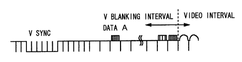
Figs. 1A and 1B show waveform diagrams of the V blanking
interval and a waveform diagram of a lock flag. Data A
is inserted in the V blanking interval of a television
signal as shown in Fig. 1A. Data A is stored in a
memory in the decoder. When the V blanking interval is
finished, the decoded data is read out and a
predetermined process is executed by a controller. In
1
case of storing the data into a memory, if a PLL
circuit is not locked, data A cannot be correctly
sampled. Therefore, in order to confirm a locking
state of the PLL circuit, a lock flag is referred. A
waveform of the lock flag is shown in Fig. 1B. The
lock flag is a flag indicating whether the sampling
clock formed by the PLL circuit is correct or not. In
this instance, it is assumed that the lock flag simply
indicates the present locking state of the PLL circuit.
When the PLL circuit is locked, its level is set to the
H level. When the PLL circuit is not locked, the level
is set to the L level.
The actual data process is executed after the
end of the V blanking interval. The lock flag is
referred after the V blanking interval. Therefore, the
locking state of the PLL at a time point when the lock
flag is referred is merely known and the locking state
in the V blanking interval cannot be known. For
example, in Fig. 1A, in the case where the PLL circuit
is in an unlocked state when the data A is sampled and
the PLL circuit enters a locking state before the lock
flag is referred, a data process is executed in spite
of the fact that the data A is not correctly sampled.
OBJECTS AND SUMMARY OF THE INVENTION
In order to prevent such a data process, it is
necessary to continuously refer to the lock flag in the
2
~15~~14
V blanking interval or a flag to judge whether the PLL
has been performed at that time or not every data is
needed. However, according to such a method, the
process is complicated.
It is, therefore, an object of the invention
to provide a data extracting apparatus which can decode
only data sampled by a correct sampling clock.
The invention relates to a data extracting
apparatus for extracting data multiplexed in a
predetermined interval of a video signal, comprising: a
PLL circuit for generating a sampling clock locked with
a sync signal in the video signal and for generating a
flag indicating whether the sampling clock is correctly
locked with the sync signal or not; and a memory for
storing the data sampled by the sampling clock, wherein
the sampled data is made valid or invalid on the basis
of a status of the flag.
The sampling clock locked with the sync
signal in the video signal is generated and the lock
flag indicating a locking state of the PLL circuit 5 is
also generated by the PLL circuit 5. The data in the V
blanking interval is sampled by the sampling clock and
is stored in the memory 7. A controller 2 detects a
status of the lock flag. When the lock flag is at the
H level, the data stored in the memory 7 is made valid,
and when it is at the L level, the data is made invalid.
According to the invention, in the case where
3
~153~I4
the PLL is unlocked in the V blanking interval, since
the lock flag is held at the L level, it is possible to
know that the data was not sampled by the correct
sampling clock even if the lock flag is referred after
the end of the V blanking interval. Further, in the
case where the lock flag is at the H level by referring
to the lock flag after the end of the V blanking
interval, a fact that the PLL has been always locked in
the V blanking interval can be guaranteed. Therefore,
only the data which was correctly sampled can be
processed in a locking state of the PLL.
The above, and other, objects, features and
advantage of the present invention will become readily
apparent from the following detailed description thereof
which is to be read in connection with the accompanying
drawings.
BRIEF DESCRIPTION OF THE DRAWINGS
Figs. 1A and 1B are waveform diagrams of the V
blanking interval and waveform diagram of the lock flag
which are used for explaining a prior art;
Fig. 2 is a block diagram of a data extracting
apparatus according to the invention;
Fig. 3 is a block diagram of a locking state
detecting circuit;
Figs. 4A, 4B and 4C are waveform diagrams of
a lock flag obtained by the data extracting apparatus.
4
~1~3214
Fig. 5 is a flowchart regarding the operation
after a V blanking interval of the data extracting
apparatus.
DETAILED DESCRIPTION OF THE PREFERRED EMBODIMENTS
A data extracting apparatus according to the
invention will now be described hereinbelow with
reference to the drawings. Fig. 2 is a block diagram
of the data extracting apparatus. The data extracting
apparatus comprises a V blanking general decoder 1 and
a controller 2. Video data is supplied to a sync
separator 3 and a sampling circuit 4 of the V blanking
general decoder 1. An H sync and a V sync in the video
data are separated by the sync separator 3. The H sync
and V sync are supplied to a PLL circuit 5. On the
other hand, parameters such as sampling clock
frequency, line number, and the like are set by the
controller 2. The parameter set values are supplied to
a register 6.
The parameter set values are supplied from the
register 6 to the PLL circuit 5 to which the H sync and
V sync were supplied. The PLL circuit 5 generates a
sampling clock locked with a sync in accordance with
the parameter set values. The sampling clock is
supplied to the sampling circuit 4. The parameter set
values are supplied to the sampling circuit 4 from the
register 6. The sampling circuit 4 samples the data of
a line designated by the parameters by the designated
number of bits on the basis of the sampling clock and
the parameter set values. The data sampled by the
sampling circuit 4 is stored in a memory 7. The stored
data is read out by the controller 2.
The PLL circuit 5 outputs a lock flag at the H
level indicating a locking state to the register 6. In
case of the lock flag of the H level, the data stored
in the memory 7 is made valid. The lock flag is
outputted to the controller 2 from the register 6.
Thus, the controller 2 can confirm that the data in the
V blanking interval read out from the memory 7 was
sampled by the correct clock. When the PLL circuit 5
is not locked with the sync, a correct sampling clock
is not generated. Therefore, the lock flag of the L
level is generated to the register 6 from the PLL
circuit 5. In case of the lock flag of the L level,
the data stored in the memory 7 is made invalid. When
the V blanking interval is finished, V blanking end
data is supplied to the controller 2 from the V
blanking general decoder 1.
Fig. 3 is a block diagram of a locking state
detecting circuit to output the lock flag to the
register 6 from the PLL circuit 5. This circuit is
constructed by an AND gate 13, an NOT gate 14, and a D
flip-flop 15. A lock status flag indicating a locking
state is generated from one input terminal 11 of the
6
~~.~~1
AND gate 13. The locking status flag is also supplied
to the NOT gate 14. A V sync in the video data is
inputted from another input terminal 12 of the AND gate
13. An inverted output of the AND gate 13 is supplied
to a set terminal Set of the D flip-flop 15. On the
other hand, an output of the NOT gate 14 is supplied to
a reset terminal Reset of the D flip-flop 15. The lock
flag is outputted to a register (not shown) from a D
output terminal of the D flip-flop 15.
Figs. 4A, 4B and 4C are waveform diagrams of
the lock flag obtained by the data extracting apparatus
according to the invention. In order to explain the
waveform of the lock flag, a waveform diagram of the V
blanking interval and a waveform diagram showing the
locking state of the PLL circuit are shown. In the
case where the PLL circuit is locked as shown in Fig.
4B with a V sync of the V blanking interval as shown in
Fig. 4A, the lock flag is set to the H level at a start
point of the V sync. When the PLL circuit is unlocked
in the V blanking interval, the lock flag is set to the
L level synchronously with the unlocking. Accordingly,
the data that is outputted from the D terminal of the D
flip-flop is set to the L level.
Namely, in the case where the PLL is unlocked
in the V blanking interval, since the lock flag is held
at the L level, even if the lock flag is referred after
the end of the V blanking interval, it can be
7
recognized that the PLL was unlocked in the V blanking
interval. When the lock flag is at the H level at a
time point when the lock flag is referred after the end
of the V blanking interval, it is assured that the PLL
has been always locked in the V blanking interval.
Therefore, only the data which was correctly sampled
can be processed in a locking state of the PLL.
Fig. 5 is a flowchart regarding the operation
after the end of the V blanking interval of the data
extracting apparatus. In step 21, a check is made by
the controller 2 to see if the V blanking interval is
finished or not. When the V blanking interval is not
finished, after the lock flag which is supplied to the
register 6 from the PLL circuit 5 was set to the H
level (step 25), a processing routine is returned to
step 21. On the other hand, when it is judged in step
22 that the V blanking interval was finished, step 22
follows. In step 22, it is judged whether the PLL
circuit 5 has been locked or not (the lock flag is at
the H level or not). When the lock flag is not at the
H level, since this means that the PLL is unlocked in
the V blanking interval, the process is finished. On
the other hand, in step 22, when it is judged that the
lock flag is at the H level, the data written in the
memory 7 is read out (step 23) and a predetermined data
process is executed (step 24).
Having described a specific preferred
8
~1~3~1~
embodiment of the present invention with reference to
the accompanying drawings, it is to be understood that
the invention is not limited to that precise embodiment,
and that various changes and modifications may be
effected therein by one skilled in the art without
departing from the scope or the spirit of the invention
as defined in the appended claims.
9