Note: Descriptions are shown in the official language in which they were submitted.
CA 02153345 1999-02-26
LOW POLARIZATION SENSITIVITY GOLD MIRRORS ON SILICA
Technical Field
This invention concerns gold mirrors on silica surfaces, such as on an
inclined
end section surface of an optical fiber.
Background of the Invention
Optical transmission properties of silica make it the material of choice for
infrared fiber-optic communication systems. Reflective properties of gold in
the infrared
make it the metal of choice for making a mirror with low polarization
sensitivity.
Unfortunately, gold does not adhere well to silica, so if a gold mirror is
needed on a silica
surface, such as an end of a silica fiber or a waveguide, then an adhesion-
promoting layer
must be applied before the gold is deposited. One commonly employed approach
utilizes
consecutive depositions of layers of titanium and platinum on the silica
surface before
applying the gold. These layers are, however, optically opaque due to their
thicknesses needed
to produce sufficient gold adhesion promotion, which are typically on the
order of 100-200
nanometers (nm).
Summary of the Invention
A thin metallic adhesion layer which is virtually optically transparent in the
infrared is deposited by aqueous chemistry on a silica surface. Subsequent
deposition of gold
on the adhesion layer by e-beam evaporation produces a gold coating that
adheres well and
makes a gold mirror on the silica. The metal adhesion layer comprises nickel
deposited in a
thickness sufficient to enhance adherence of gold to the surface of silica but
insufficient to act
as a barrier to the passage of infrared radiation to and from the gold layer.
In accordance with one aspect of the present invention there is provided a
gold
mirror for reflecting radiation to or from a silica article comprising: a
silica article including
a surface; a gold layer; and a nickel layer, said nickel layer forming an
adhesion layer between
said surface of said silica article and said gold layer; wherein said nickel
layer is deposited on
said surface of said silica article by electroless plating, and said nickel
layer has a thickness
such that said nickel layer is substantially transparent to infrared
radiation; and wherein said
nickel layer further comprises a nickel-phosphorous (Ni-P) alloy.
CA 02153345 1999-02-26
- la-
In accordance with another aspect of the present invention there is provided a
gold mirror on a silica article for reflecting radiation of wavelength between
about 550 nm
and about 850 nm from the silica article, comprising: a gold layer; and a
nickel layer forming
an adhesion layer between a surface of said silica article and said gold
layer; wherein said
nickel layer is deposited on said surface of said silica article by
electroless plating, and said
nickel layer has a thickness such that said nickel layer is substantially
transparent to infrared
radiation, and wherein infrared radiation passes through said silica article
and said nickel
layer substantially without being absorbed and the infrared radiation is
reflected by said gold
layer.
Brief Description of the Drawings
FIG. 1 is a schematic representation of a single optical fiber with a 45
° mirror
and a surface emitting laser (SEL) arranged for injecting radiation toward the
mirror or
alternatively a photodetector for receiving radiation from the mirror;
FIG. 2 is an exploded side view of the end portion of the optical fiber shown
in
FIG. 1 representing the silica mirror surface, a metal adhesion layer and a
gold mirror layer;
FIG. 3 is a side view of a fiber array block with a plurality of optical
fibers
supported in a preset relation to a SEL chip provided with a corresponding
array of SELs;
FIG. 4 is a schematic perspective representation of the array block showing
mirror-carrying fiber ends;
-2-
FIG. 5 is a schematic representation of apparatus in a flow chart scheme
for producing the metal-deposition steps in the formation of mirrors on silica-
surfaces;
FIG. 6 is a plot of absorbance versus wavelength in nanometers for a
silica slide coated on both sides with a nickel layer after treatment for 20
seconds in
an electroless Ni solution at 35°C;
FIG. 7 is a plot of calculated reflectance at silica-nickel interface versus
an angle of incidence (in degrees) at 850 nm wavelength, with n o = 1.46, n =
2.58
and k = 4.55; and
FIG. 8 is a plot of calculated reflectance at silica-gold interface versus
an angle of incidence (in degrees) at 850 nm wavelength with n o = 1.46, n =
0.08
and k = 4.98;
Detailed Description
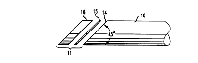
In FIG. 1 of the drawing is shown schematically an end portion of an
optical fiber, 10, provided with a mirror, 11, and a beam of radiation, 12,
propagating
from or to an optical device, 13. Beam of radiation 12, propagating from
device 13
acting as a source of radiation, such as a laser, impinges upon and is
reflected from
the mirror into the optical fiber. Conversely, the beam of radiation
propagating
through the fiber, will impinge upon the mirror and will be reflected out of
the fiber,
e.g., toward device 13 acting as a detector of radiation, such as a
photodetector. For
good coupling into and from the optical fiber, high reflectance mirror is
needed.
This characteristic is provided by mirror 11 deposited on a surface, 14, of
the optical
fiber. The mirror includes an adhesion-promoting (or glue) layer 15, and a
reflective
gold layer, 16, as is shown in an exploded view of FIG. 2.
In accordance with this invention, glue layer 15 is a thin layer
comprising nickel. As deposited from a hypophosphite-containing electroless
nickel
solution, a nickel-phosphorus alloy (Ni-P) is produced. The glue layer is
deposited
in a thickness sufficient to enhance adhesion of gold to the silica surface of
the
optical fiber but insufficient to act as a barrier to the passage of infrared
radiation,
e.g., at 850 nm, to and from the gold layer. After sensitization of the silica
with
SnF2 and activation with PdCI Z /HCI, Ni-P is deposited in the electroless
bath
through a nucleation and growth mechanism, detectable by atomic force
microscopy
(AFM). Once the activated silica is placed in the nickel bath, Ni-P begins to
deposit
at scattered nucleation sites and grow laterally until these "islands"
coalesce to form
a continuous surface of Ni-P. Growth normal to the surface presumably occurs
simultaneously. Since the deposition of gold directly onto the activated sub-
layer,
CA 02153345 1999-02-26
-3-
without any nickel, results in poor adhesion of gold, it is assumed that the
best case for good
adhesion of gold occurs once the nickel layer becomes continuous.
It is not necessary to assume a morphology, however, to describe the deposited
Ni-P layer. From a practical perspective, the amount of Ni-P can be
characterized in terms of
the absorbance at a given wavelength. "Absorbance" is defined in the usual
way, viz.
A = - log of T, where T = I/Io is the transmittance. As can be seen from FIG.
6, the absorbance
increases with decreasing wavelength. By using a spectrophotometer to measure
the
absorbance of the layers deposited on both surfaces of a quartz slide, it is
possible to correlate
the absorbance at, for example, 550 nm (or any other easily accessible
wavelength) with an
amount of Ni-P deposited necessary to provide good adhesion. It is observed
that if the
absorbance of these two layers, as deposited on the quartz slide, is > 0.008
at 550 nm
(0.003 at 850 nm) then sufficient adhesion to gold is achieved. The preferred
absorbance
range is 0.011-0.013 at 550 nm (0.004-0.005 at 850 nm). These absorbances
include a
small contribution from the Pd-containing sensitization layer of about 0.0006
at 550 nm
(0.0002 to 850 nm).
Prior to sensitization, the optical fibers are cleaned and polished so as to
provide
end surface 14 with a 45 ° slope. The reason for selecting a 45
° angle may be explained as
follows. It might appear that total internal reflection in a fiber would be
sufficient to make
good mirrors out of the angled fiber ends; unfortunately, the total reflection
angle for silica is
only about 43 °, and the angular spread of the light incident on the
mirror is likely to be
considerably more than ~2°. At incident angles less than the critical
angle, the
internal reflectance of a dielectric is low and strongly polarization
dependent. However, for
good coupling high reflectance is needed. In addition, it is also important to
avoid a strongly
polarization or position dependent reflectance that could convert laser mode
or polarization
fluctuations into amplitude noise. These considerations make it necessary to
have an efficient
reflecting coating with low polarization sensitivity on the 45 ° fiber
ends.
The reflectance of a silica-metal interface may be calculated using the
Fresnel
formulas for reflection at an interface,
CA 02153345 1999-02-26
-4-
no cos ~N cos B no cos BN cos ~
r =
r" no cos ~ + N cos B ' ~ no cos 8 + N cos ~
And R~,~. - Ir~,~ (2
where R is reflectance, 8 is the angle of incidence in the first medium, ~ is
the refraction
angle in the second medium given by Snell's law, no is the index of refraction
in the first
medium, N is the index of refraction in the second medium, rn and ra are
reflection amplitudes
and ~ and a indicate the two polarizations. For the silica fiber no was taken
as 1.46 and the
components of the complex refractive index N = n + ik for different metals
were obtained. J.
H. Weaver et al., ed., "Physics Data: Optical Properties of Metals,"
Fachinformationszentrum,
Karlsruhe, 1981, Vol. 18-1, pages 36, 62 and 106, and Vol. 18-2, pages 59 and
75.
Metals that adhere well, such as titanium and chromium, are poor reflectors,
having reflectances of only 0.43 and 0.51 at 850 nm, respectively. While
aluminum averages
0.82 at 850 rnn it is not suitable as a low polarization sensitive mirror
since its two
polarizations are differing by 13%. Nickel which has an average reflectance
near 45 ° of less
than 0.6 (FIG. 7) is also a poor reflector. FIG. 8 shows the calculated silica-
gold reflectance at
850 nm versus angle of incidence for the two polarizations. Near 45 °
the average reflectance
is ~98%, and the two polarizations differ by only ~ 1%. It is clear that
except for its adhesion
properties gold is the best metal for the mirror on silica.
After the polishing step, end surface 14 of the fiber is cleaned, primarily to
remove the residues remaining from the polishing step. The cleaning may be
conducted in a
hot sulfuric acid; alternatively, the residues could be removed by immersion
in 18 MS2 water
with ultrasonic treatment for 10 minutes, followed by blowing dry with
nitrogen. Thereafter,
fibers are put into a Ultra-Violet Ozone Cleaning System (UVOCS), Model T10X10
OES, for
10 minutes.
Glue film 15 is deposited on polished and cleaned surface 14 of the optical
fiber
followed by formation of gold layer 16 on the glue film. A feasible process
for depositing
adherent nickel deposits on silica is known in the prior art. That process may
be used with
certain modifications to deposit the nickel-containing glue layer.
The deposition process of the glue film includes immersion of the polished and
cleaned surface 14 of the silica-containing optical fiber into an aqueous
solution of SnF,, 51,
within a container, 52, overflow rinse 53, immersion of the sensitized end
into an activating
CA 02153345 1999-02-26
-S-
aqueous solution of PdCIZ and HC1, 54, within a container, 55, overflow rinse
56, and
immersion into an electroless nickel plating solution, 57, within a container,
58, for a period
sufficient to produce a desired absorbance, followed by a rinse, 59, within a
container, 60, and
blow drying the nickel-coated end by an inert gas, such as nitrogen, supplied
from a nozzle,
61. The dried nickel-coated surface is then placed into a vacuum chamber, 62,
for e-beam
deposition of gold layer, 16.
SnFz solution, 51, contains from 0.5 to 3 g/L, preferably 1.0 g/1 SnFz. PdCl2
solution, 54, contains from 2 g/L to 10 g/L, preferably 6 g/L PdCl2 in dilute
HCl (from greater
than O.OO1M to less than O.1M, preferably 0.02M HC1) with pH range up from 1.6
to 1.7. All
rinses, and especially the rinse following the sensitization step, are
conducted with deionized
water.
The deionized water rinses 53 and 56 after the SnF2 and PdCl2 steps are short,
about 20 second overflow rinses. The overflow was achieved by pumping the
deionized water
into the bottom of containers, 63 and 64, respectively, each positioned within
a larger
overflow-catching container, 65 and 66, respectively. The water overflowed
into the larger
container from which it was recirculated. The pumping was conducted with a
Cole-Parmer~
peristaltic pump and Masterflex~ type 6412-16 tubing (Viton~) at a flow rate
of about 230
ml/min. Alternatively, any pump which does not contaminate the water can be
used to create
an overflow rinse. The SnFz rinse container 63 was equipped with a fine
porosity sintered
glass frit, 67, for deoxygenating the water with bubbled inert gas, such as
nitrogen. The
nitrogen bubbling was discontinued during the overflow rinse. The process up
to and
including the PdCl2 step was carried out under nitrogen atmosphere, such as
inside a
Plexiglass nitrogen containing box, 68. Beginning with the PdClz rinse step,
all processing
was carried out under air, so no frit was necessary in rinse container, 64.
After PdCl2 rinse 56 the fiber is transferred to electroless nickel bath, 57.
The electroless nickel plating solution was a commercially obtainable solution
provided as
two separate parts, part A and part B, which are to be combined prior to use.
Part A is a
source of nickel ions, such as nickel chloride, nickel sulfate and nickel
acetate, and part B is a
source of hypophosphite ions (a reducing agent) such as sodium hypophosphite.
One type of
nickel plating solution is obtainable from Fidelity Chemical Products
Corporation, Newark,
NJ, as type 4865 in which part A contains nickel sulfate and part B contains
sodium
hypophosphite, sodium hydroxide and acetic acid. The nickel solution is
prepared by
combining part A, part B, and water, the solution having pH ranging from 4.5
to 5.2. The
CA 02153345 1999-02-26
-6-
nickel solution for use in this metallization process was prepared by
combining part A, part B
and 18 MS2 water in the ratio 1:3:16, then filtering using the Halgne Media-
Plus~ filter unit
(nylon 0.2 micrometer pores). The pH of this solution was about 4.85. The
electroless nickel
solution was maintained at 351 °C and the plating time was chosen to
range from 30-60
seconds. These times correspond to the deposition of Ni-P films having an
absorbance of 0.01
at 550 mm when measured for the Ni-P and gold layers.
After nickel (Ni-P) deposition, the samples were dipped into D.I. water rinse,
59,
blown dry with nitrogen at 61, and mounted in a vacuum chamber, 62, for
electron beam
(e-beam) deposition of gold. The gold layer was deposited in a thickness from
100 to 150 nm.
Thicknesses less than 100 nm may lead to inferior mirror interface, while
mirrors thicker than
150 nm are uneconomical leading to waste of gold. Preferred thickness lies
around 120 nm of
gold. To reduce the possibility of formation of nickel oxide on the Ni-P film,
samples are
placed under vacuum, typically within less than 1 hour after the drying with
nitrogen.
Adhesion was evaluated by applying Scotch Magic Tape~ to the gold surface and
peeling the tape off. If the gold remained on the substrate the adhesion was
considered
satisfactory. In order to facilitate adhesion testing, the mirrors were
produced on relatively
large silica slides ( 1 " X 1 " X 3 mm) purchased from National Scientific,
Quakertown,
PA. These slides also had an index of refraction, no, of 1.46. The slides were
also used for
optical absorption measurements. The slides were coated on one and on both
major surfaces
by a process similar to that used for producing mirrors on the ends of optical
fibers except
that there was no need for producing 45 °-slanted surfaces. Prior to
coating the slides with an
adherent metal layer comprising Pd and Ni-P films, each of the slides was
cleaned by
immersion in sulfuric acid at 150°C, cooled to room temperature, rinsed
in 18 MS2 water, and
blown dry with nitrogen. Optical absorption measurements were performed on the
slides
using a Varian Cary 219~ spectrophotometer. The absorbance vs wavelength is
shown in FIG.
6. The baseline was recorded using clean quartz slides in both beam paths. To
measure the
absorbance, the metal layer comprising Pd and Ni-P films was deposited on both
sides of the
slides. Immediately after measuring the absorbance of the Pd/Ni-P layer, the
samples were
mounted in a vacuum chamber for e-beam deposition of gold.
An accurate determination of the absolute reflectance of the gold mirror on
silica
fibers is difficult. However, a measurement of the ratio of the reflectances
was made for the a
and ~ polarizations. The a/~ ratio in two measurements was found to be 0.983
and 1.020,
which are within measurement error of the calculated value of about 1.012. In
any case, the
CA 02153345 1999-02-26
polarization difference is sufficiently small. Incidentally, while the actual
magnitude of the
reflectance was not measured, it is deduced that it is likely to be at least
~96% from the
observation that the difference between unity and the a reflectances is always
comparable to
the difference between the a and ~ reflectances. It is concluded that the
optical performance
of this gold mirror is not significantly impaired by the very thin adhesion
layers used in this
process.
This process is useful to make gold mirrors on the ends of optical-fibers for
use
in a multiple optical fiber array schematically shown in FIGS. 3 and 4, such
as in the
transmitter or receiver portion of the Optoelectronic Technology Consortium
(OETC) high
performance data link. The latter uses an optical data bus in the form of a
fiber array block,
31, consisting of 32 parallel multimode fibers 10 each capable of carrying 500
Mb/s.
Transmitter and receiver modules, 32, are identical in optical design and
mechanically very
similar. The transmitter uses, for example, a GaAs vertical cavity surface
emitting laser
(VCSEL) array operating at 850 nm, with beam of light 12 (FIG. 1) vertically-
emitted from
the lasers reflected into an array of 32 horizontal optical fibers 10 by 45
°mirrors 11 on the
polished ends of the fibers. This array of 45 ° polished fibers 10 is
sandwiched between two
silicon chips, 33 and 34, with etched v-grooves, 35, to position the fibers at
the correct pitch,
p, of 140 ,um (see FIG. 4). This fiber array block assembly connects directly
to a 32-fiber
cable via a connector (not shown), such as a modified AT&T MAC II~ connector.
The
receiver uses a similar optical fiber array, except that the array of VCSELs
is replaced by an
array of photodiodes.
In the preceding pages, the process of producing mirrors was described with
reference to treating single or bunched optical fibers. A preferred technique
would be to place
fibers 10 into the grooves of fiber array block 31, polishing the ends of the
fibers to the 45°
angle, cleaning the polished ends and then to deposit the glue film and the
gold minor on the
ends of the assembled plurality of the fibers.