Note: Descriptions are shown in the official language in which they were submitted.
WO95/15639 21~ PCT/US94/12280
METHOD AND APPARATUS FOR MULTI-PHASE COMPONENT
DOWNCONVERSION
Background of the Invention
1. Technical Field of the Invention
The present illvelllion relates to digital downconversion and, more
partic~ rly, to a method and a~aralus for multiphase component
downconversion.
2. Des~ lion of the Related Art
In a radio transmission system a transmitter generates digital
symbols from digital data and transmits such symbols for the benefit of a
receiv,2l. The channel can be wireless or wired. If the channel is a radio
frequency (RF) wireless channel, time dispersion can be introduced into a
signal before reception at the receiver. Fading, cochanel and adjacent
channel inlel~rellce and noise can also be introduced into the signal.
A transmitter generates an output such as digital symbols S(n). The
received signal is filtered and sampled to produce a received digital signal
y(n) which is sent to a demodulator (e.g. a channel equalizer). For any type
of signal modulation (e.g. FM, QPSK, OQPSK, r~/~DQPSK, GMSK, DS-
CDMA) where a quadrature representation of the signal is desired, at the
2~ receiver it is rlecess~. y to provide for quadrature downcol.version and
~limin~tion of signal imp~irm~nts caused by the receiver and the channel.
~ A TDMA (Time Division Multiple Access) radio transmission is a
time-shared trarlsmission on se~aldle timeslots 1 to N. A TDMA radio
tra~smi~sion can be on a single frequency carrier. A different signal
sequence SS, which includes a synchronizing sequence SO and a data
sequence DO with the inform~tion to be tral.~n~ille~i, can be transmitted in
wo ss/ls63s 2 lS 3 6 8 ~ 2 - PCT/US94/12280 .~
each *meslot. The signal sequence SS contains a binary signal, although
the aforesaid symbols S(n) can be coded accorling, for instance, to the
QPSK-code. In a complex ~llmh.or plane, with axes designated I and Q,
four possible values of the symbols S(n) are m~rkell one in each quadrant
s with the binary numbers 00, 01, 10, or 11.
A spread spectrum DSCDMA (Direct Sequence - Code Division
Multiple Access) radio ka~ ission system kansmits to all users at the
same time and on the same channel frequency by spreading each user's
signal sequence SSi with a pseudonoise (PN) sequence PNi~ (~denotes
0 complex conjugate). Each user's signal sequence is spread in such a
manner that each signal can be uniquely despread at the receivel by using
the co,les~onding synchronous PN sequence, PNi, while at the same time
reducing the other users signals (i"lelfel~:llce) so that the signal quality is
not impaired. In addition to, or in place of the PN sequences, a signaling
set consisting of Walsh sequences can be used to further rliccrin inate
between user's signals (spread and despread) as is described, for example,
in TIA/EIA IS95 Mobile Station-Base Station Compatibility Standard for
Dual-Mode Wideband Spread Spectrum Cellular System.
In a receivel there are many ways that a direct cullel~l (DC) or
carrier error term can be introduced in the desired signal. In the b~seb~nd
circuitry a DC term can be introduced due to oper~ onal amplifier offsets,
demodulator offset voltages, and/or analog-to-digital converter
rh~r~cteric1irc. Likewise, since a coherent local oscillator (L.O.) is required
for demodulating the desired signal to b~ceb~nd, there can be self-
demodulation of any local oscill~tor leakage which would then produce a
b~cebAnd DC error term. If the received signal is converted to an
intermediate frequency (IF) and then digitized, a similar phenomena can
illlr~ ce errors especially when the local oscillator's frequency or
irlt~ te frequencies are chosen to be either coherent or related to the
30 bit rate (often done to simplify the sampling and proces~ , of the signal).
wo 9S/15639 21 ~ 3 ~ 8~ PCT/US94/12280
For most ~y~lwlls the DC error term (as well as any DC term which is part
of the desired signal) can be elillullaled by alternating current (A.C.)
coupling with a cut-off frequency s~ iPntly low so as not to appreciably
effect the collLelll of the desired signal. However, if the receiver is
5 automatic gain controlled, then the A.C. coupling will most likely not
prove e~eclive because the DC offset will be dynamic and most likely at a
rate above the A.C. coL-~lil,g cut-off frequency. This is the case in a TDMA
system. In a code division multiple access (CDMA) system the DC offsets
can be especially troublesome since the bAcebAnd signal has inherent DC
o terms which must be present to successfully demodulate the signal where
the addition of other DC terms would gleally degrade demodulation
performance.
Automatic gain control (AGC) can be used in a receiver to limit the
required dynamic range of a receiver. Among other things, automatic
5 gain control will limit a number of required analog-to-digital converter
bits. Usually, in a TDMA system, it is desired to track signal attenuation
due to lognormal fading (shadowing) rather than Rayleigh fading (fast
fading). In a CDMA system, automatic gain control (AGC) sets the
variance of the resultant white noise resembling composite signal as seen
20 by the analog-to-digital collv.,l~l.
Receive~ typically ~ quadrature downcollvelsion upon
feceived signals modulated in a complex plane. Quadrature
downconv.l~ion can be ~l~lmed in analog receivel~ or digital receivers
such as TDMA and CDMA receivels. Quadrature downconversion from
2s an intPrlne~liAte frequency (IF) is collvelllionally pel~lllled, for example, in an analog rec~ivel, by iul~llLIg a pA~sbAnd analog signal into two
analog mixers in parallel followed by lowpass filters to eliminate double
frequency signal colll~ollenls. Analog-to-digital converters are used to
sample the resllltAnt analog in-phase and qtlA-lratllre bA~eb~nd signals.
2 ~53~
- 4 -
Various types of digital quadrature downconv~ ls can also be
implemented. One advantage of these digital downconverters over the
analog downcollveller is a reduction in the number of analog-to-digital
converters required. A first type of digital downconverter, for example,
5 requires a high speed analog-to-digital converter, followed by two digital
mixers and de~im~tion filters. Such an implementation is provided, for
example, in Harris Part No. HSP 50016. A second type of digital
downconverter also uses one analog-to-digital converter. The sampling
frequency (fs) and final i~termecli~te frequency (fIF) are chosen such that
0 the samples of the signal need to be alternatingly fed with colles~onding
sign changes to two digital lowpass interpolating filters to obtain the
desired in-phase and quadrature b~ek~nd signals. Such a digital
downconverter is provided, for example, in Harris Part No. 43216 or by L.
E. Pellon, "A Double Nyquist Digital Product Detector for Quadrature
Sampling", IEEE Transactions on Signal Processing, July 1992, pp. 1670-
1681.
Another type of digital downcollvel~ion uses a discrete-time Hilbert
filter together with a complex downconverter state. Such a type of Hilbert
downconverter is described in "Ouadrature sampling with high dynamic
20 range", IEEE Transactions Aerospace Electronic Systems vol. AE8-18, no. 4,
pp. 736-739, November 1982.
Such a type of ~lbert downcol,v~.lel also uses one less analog-to-digital
coll-~ellel than the analog downconverter. One less analog-to-digital
collv~ller allows one less receivel branch providing better gain balance
25 between the in-phase and quadrature signal. The phase accuracy and gain
balance of a Hilbert downconverter between the in-phase and quadrature
signal components is also more accurate and not sensitive to temperature
variations or aging (component drifting).
The above-mentioned first digital downconverter requires a much
30 higher speed analog-to-digital converter than the analog downconverter.
~4
WO95/15639 21 53 6 8 2 pcTluss4ll228n
Also, the first digital downcollverlel requires actual high speed
multiplication for mixing down the signal to extract the in-phase and
quadldlure b~ceb~nd signals. The second digital downconverter does not
c require a high speed analog-to-digital COnVe1le1 or high speed
5 multiplication because it uses a multiplierless final downconversion stage.
The second digital approach, however, requires exp~nsiv-e A/D converters
because of the required sampling rate. The Hilbert downcollv~llel
requires a complex mixing stage to ~ifolll- downconversion. Expensive
hardware or e~clel~ive processor time must be used to multiply the
o complex numbers.
S~mm~ry of the Invention
The present invention solves these and other problems by
5 providing a method and apparatus for multi-phase component
downconv~l~ion. An analog-to-digital co,lv~ r is provided to receive an
i~terme~ te frequency signal and provide a digital signal at a sampling
rate. A Hilbert trallsfolll~dtion network provides a p~sb~nd quadrature
colll~ol.ent based on the digital signal provided from the analog-to-digital
20 collvellt:l. A delay element provides a passband in-phase component
based on the digital signal from the analog-to-digital CO1IV~1Iei. A digital
translator alters the p~cb~rld quadrature and in-phase components from
the Hilbert lldl~"l,ation network and the delay element based on a
predel~ ....i.~ed ~aLI~l, to provide the downconve,led b~seb~nd
25 quad,dl~re and in-phase signals. Accordil~g to the diffeielll embodiments,
the digital translator is provided by a pseudorandom sequence
demodulator. The digital translator can also be accompanied by early and
late translators for downconverting code division multiple access (CDMA)
signals. An alltoIn~tic gain control circuit can be provided for
30 downconverter gain control. A direct ~;ull~nt (DC) estimator can also be
WO 95/15639 ?., ~ S3 6 6 - PCTIUS94/12280 .
provided to perform a DC estimation adjustment on the baseband
quadrature and in-phase signals.
These and other constructions and feal-lres of the present invention
will become more s~alellt from the following detailed description when -' read in conjunction with the accolll~al-yillg drawings.
Detailed Description of ~e D-d~ S
FIG. 1 illustrates a schematic block diagram of a first embodiment of
0 a method and ap~ara~us for multi-phase component downconversion
according to the present invention.
FIG. 2 illustrates a sc~m~*c block diagram of a second embodiment
of a method and apparatus for multi-phase component downconversion
utilizing a decimator with one type of DC estimation and with automatic
gain control according to the present invention.
FIG. 3 illustrates a schematic block diagram of another type of DC
estimation accordillg to the present invention.
FIG. 4 illustrates a schematic block diagram providing details of one
type of automatic gain control accordil~g to the present ill-ven~ion.
FIG. 5 illustrates a schematic block ~ gr~m of additional early and
late translators used for downcollv.rsion of a code division multiple
access (CDMA) signal according to the present inv~llLion.
FIG. 6 illustrates a diagram for one example of a translator in a code
division multiple access (CDMA) downcollvellel according to the present
invention.
WO 95/15639 ~1~ PCT/US94112280
-
De~ile-l Der~;~l;on of the P~ef.,.~ Embo~imf~nt~
The present invention provides a quadrature downconverter
~ having multiplierless downconversion stages and needing only one
5 analog-to-digital collvellel. One less analog-to-digital conv~llel is needed
than the two analog-to-digital collv~ used for the two analog receiver
branches of the analog downcoll-v~llel. A lower frequency sampling rate
can also be used for the analog-to-digital con-vt:lle~. A multiplier is also
unrPcess~.y in the present illvel~lion as was r~c~s~ry in the first digital
0 downconvellel. The sampling rate fBAUD is set to an inleglal multiple of
the intermediate frequency fIF to provide these benefits. Better gain
balance between the in-phase and quadrature signal and low amplitude
ripple are also achieved by the present invention. Furthermore, phase
accuracy and gain balance between the in-phase and quadrature signal
5 com~ol-ents are ill,~roved without temperature or aging sensitivity.
The present illvenlion further using a Hilbert filter has an
i*onal advantage over the other known digital approaches. The
present illvenlion takes advantage of a trade-off between 90~ phase
accuracy, bandwidth and the number of filter taps. In the present
20 il~velllion, the filter can be implemented with as few as four taps per
output point pair (4x oversampling), or can be rur~ at half the clock speed
with a ~lerim~tor (2x c~velaam~ling) by choosing the Hilbert filter order to
be odd. Additionally, the sampling rate and the final intermediate
frequency fIF can be chosen to minimize the amount of computation
25 needed for a de-~im~tor to ~e~im~te the signal to T-spaced samples, where
1/T=fBAUD is the baud (symbol) rate. That is, fs=4flF as before, but with
the additional col~sllaint that fIF=fBAUD such that the decimation is just a
sample s~ ion process with no decimation filter needed.
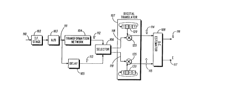
FIG. 1 illustrates a receive~ 100 that includes a downconve.lel after a
30 final irterme~ te frequency (IF) stage 102. The downconverter indudes
wo 95/15639 2~3 6 ~2 -8- PCTAUS94/12280
an analog-to-digital col,v~llel 103 with enough resolution (bits) to handle
the receiver dynamic range and meet quantization noise req~ el,lents.
The analog-to-digital converter 103 is followed by a transfolll,ation
network 104, a selector 106 and a digital translator 107. The digital
translator 107 is colll~osed of a pair of sign changing devices 125,120 and
130,135, one for each branch. A sign chal,~,in~ device contains a circular
shift re~islel 120 collldilillg the sign information and a sign changing
device for applying the sign change 125 based on the output of the
masking register of the circular shift regislel to the co~l~s~ollding
0 p~ssb~nd component. The result of the digital translator 107 is the
quad~dlule and in-phase b~ nd signal com~ollents 114 and 115. The
q~ r~lre and in-phase b~eb~nd signal coll,~ol~ents 114 and 115 are
applied to a DC estimator/rejection circuit 108. The oul~,lLs of the DC
estimator 108 are the DC free b~cebAnd quadra~ e and in-phase signal
components.
The l~C~iVel 100 receives a signal 110, which may be an analog
signal with arbitrary modulation (e.g., QPSK). This signal may also be
llal.~...ill~ by wire or lia,~...issiQn may be wireless (e.g., a RF signal).
Once r~ceived, the signal 110 is processed by a final IF stage 102 which
20 serves to translate and filter a signal from an initial or iIlt~rme~ te
frequency (IF) to another desired final intermediate frequency (IF). The
signal is also filtered to remove undesired frequency components and
reduce noise and il-lel~iellce. The final IF frequency (fIF) is chosen as a
multiple of the signal baud rate (fBAUD=1/T where T is a symbol
25 il-lelv~l). In this case the ffF is set to be equal to fBAUD for further
reduction in r~ ifed analog-to-digital conv~llel sampling rates and
required hardware clock speeds. The analog signal out of the IF stage 102 is
then sampled by the analog-to-digital collveller 103 where the sampling
rate (fs) is chosen to be 4x the final IF frequency. That is, fs = 4ffF, which
30 since ffF=fBAUD then the signal is 4x ov~l~am~led. That is, there will be 4
9 --
samples per b~c~nd T-spaced symbol. The sampled real signal 111 is
then input into the transformation network 104 to obtain the quadrature
p~csb~nd signal component 112. The trallsfollllation network 104 can be
implemented as a Hilbert tral~follll filter. Alternatively, the
5 transfollllation network 104 can be implemented as a lowpass filter and
the delay circuit as another lowpass filter. The two lowpass filters can be
those in Harris Part No. 43216 or L. E. Pellon, "A Double Nyquist Digital
Product DeleeLor for Quadrature Sampling", IEEE Transactions on Signal
Processing, July 1992, pp. 1670-1681.
The sampled real signal 111 is also sent to a delay circuit 105 where
the delay is equivalent to the group delay of the lrdl~sLolll-ation network
104. The delay of the delay circuit 105 is equal to an inlegldl number of the
samples processed by the l~dllsfollllation network 104 when, for example,
5 a Hilbert tral)sforlll filter is chosen of odd order (odd number of filter taps)
for the tral sfGllllation network 104. The output of the delay 105 is the
passband in-phase signal component 113. The selector 106 then alternately
selects quadrature 112 and then in-phase 113 passband signal component
samples to feed to the quadrature branch of the digital translator 107 and at
20 the same time alternately selects in-phase 113 and then quadrature
p~sb~nd signal component samples to input to the in-phase branch of the
digital translator 107.
The quadrature branch samples have their signs changed by a sign
changing device 125 based on the current entry in the masking register
25 (registers in bold in FIG. 1) in the circular buffer 120 containing the
quadrature translation sequence. Similarly the in-phase branch samples
have their signs changed by sign changing device 135 based on the c~
entry in the masking register in the circular buffer 130 containing the in-
phase translation sequence. These sign changing devices merely require
30 an inversion of binary bits using either digital gates or a simple operation
,.. ~
,~
WO 95/15639 PCT/US94/12280
21~6~2
- 10 -
in a microprocessor or digital signal processor. Complex multiplication
algo~ s or ~ uils are unr~Pcess~ry to merely ~- lfollll a sign change
thus saving hardware or processor time.
These sequences are derived from the complex process exp(~ k/2)
5 needed to translate the p~csb~nd signal co"l~ollents to baceb~nd signal
col~l~o~ents due to the final IF frequency and sampling frequency
relationship fs=4fIF. Note, given a complex passband signal d(kT) = I'(kT)
+ j Q'(kT) celll~led at fIF. To translate this signal to baseband requires
multiplying it by the complex ~lucess exp(j2~kfIF/fs). Since fIF/fs = 1/4
0 then the process becomes exp(jJ~k/2). Therefore, z(kT) where z(kT) =
d(kT)*exp(-jJck/2) can be written (I(O),Q(0)), (-Q(1),I(1)), (-I(2),-Q(2)), (Q(3),-
I(3)) for k=0,3 where this ~allelll of signs and I and Q ordering repeats with
this period of 4. That is,
(I(O),Q(0)), (-Q(1),I(1)), (-I(2), -Q(2)), (Q(3), -I(3))
(I(4),Q(4)), (-Q(5),I(5)), (-I(6), -Q(6)), (Q(7), -I(7))
(I(8),Q(8)), (-Q(9),I(9)), (-I(10),-Q(10)), (Q(11),-I(11))
An efficient implementation of the process exp(-j~k/2) requiring only sign
20 changes on allelllale samples can be provided by the circular bufrel~ 120
and 130. The circular buffer 120 and 130 re~e~tively contain sign changing
translation sequences (1,-1,-1,1) and (1,1,-1,-1).
The selector 106 alternately chooses samples output from the
sfolllla*on network lQ4 and the delay circuit 105. The output of the
25 quadrature branch of the digital translator 107 is the quadldl.lle baseband
sampled signal component 114 and the output of the in-phase branch of
the digital translator lQ7 is the in-phase b~ceb~nd sampled signal
component 115.
The DC estimator 108 then efficiently es*m~tes the DC (zero
30 frequency) signal components from the quadl~lule b~c~nd sampled
WO95/15639 21 S3~i~2 PCT/US94/12280
-
signal component and subtracts them to produce a quadrature baseband
sampled signal free of a DC component 116. The DC estimator block 108 at
the same time efflciently estimates the DC (zero frequency) signal
~ component from the in-phase baseband sampled signal component and5 subtracts them to produce a in-phase baseband sampled signal free of a DC
component 117. The DC estimator 108 will be ~licctl~se~ below with
refelence to FIG. 3.
The downconverter of the present invention could easily be
implemented through firmware running on a digital signal processor
o (DSP) with an internal or external analog-to-digital converter, or could
easily be il,legrdted into a single application specific inLeglaLed circuit
(ASIC) or programmable gate array (FPGA) circuit. The downconverter of
the present invention is applicable to either a TDMA or a CDMA receiver
system. For a CDMA system the translator circuit 107 could be replaced by
5 the translator circuit in FIG. 5.
FIG. 2 illustrates another embodiment of the downconverter which
includes decimator 201 to reduce the number of required operations per
output sample. The decimator 201 precedes the trallsfolll,ation network
104,105 and reduces the 4fIF sampling rate to 2fIF. Automatic gain control
20 (AGC) and DC estimation are also illusL~led as examples of other fealures
available in the various embodiments of the present invention.
The lec~iver receives a signal 110. An IF stage 102 filters and
translates the signal to a final IF equal to the signal Baud rate (fIF=fBAUD).
The signal is then gain adjusted to achieve a desired level by a digital
25 attenuator 242 which is in tum controlled by a automatic gain control
(AGC) algo,ill~ or circuit 244. The analog signal out of the digital
attenuator 242 is then sampled by the analog-to-digital converter 103
where the sampling rate (fs) is chosen to be 4x the final IF frequency as
before such that the signal is 4 times (4xj ov~ .npled.
WO 95/15639 2 i 5 3 6 ~ 2 12 - PCT/US94/12280
The decimator 201 sends even samples to the transrolll,ation
network 104 and odd samples to the delay 105. In this case the
tral~foll,lation network 104 is a Hilbert tral,sfollll filter. This is possible
because an odd order Hilbert filter is used which does not have a center
tap. The resultant pAssbAnd quadlalule 112 and in-phase 113 sampled
signal components are time aligned and 2x oversampled. Thus, there will
be two samples per bAsebAnd T-spaced symbol.
The pAssbAnd quadldlu~e 112 and in-phase 113 sampled signal
components are dire.lly input into the digital translator 107. The
0 quadrature sigl com~ollents have their signs changed in the digital
translator 107 by a sign changing device 225 based on the current entry in
the masking register in the circular buffer 220 containing the quadrature
translation sequence. Similarly the in-phase sigl components have
their signs changed by sign changing device 235 based on the current entry
in the masking register in the circular buffer 230 containing the in-phase
translation sequence. These sequences are derived from the complex
process exp(jJ~k) needed to translate the pAssbAnd signal components to
bAsekAnd sigl coll,~ol,ents due to the final IF frequency and sampling
frequency relationship fs=2fIF. An efficient implementation of the process
exp(-plk) ~ illg only sign changes can be provided by the circular
buffers 220 and 230. The circular buffer ~o and 230 respectively contain
translation sequences (-1,+1) and (-1,+1). Note the circular buffers could be
replaced by a ~lorke~ J-K flip flop. The output of the quadrature branch of
the digital translator 107 is the quadial.lle bAsebAnd sampled sigl
co~ ol,ent and the output of the in-phase branch of the digital translator
107 is the in-phase bAsebAnd sampled signal co~ nent 115.
The DC estimator block 108 of the embodiment of FIG. 2 contains
DC estimation filters 205 and 206 taking their input from the decimator
201 instead of t~e digital translator 107 as in the embodiment of FIG. 1.
The in-phase and quadrature pAssb~nd samples from the decimator 201
_ WO 95/15639 1 S36s,~? PCTIUS94/12280
- 13-
can also be viewed as alternating bAeeb~nd in-phase and quadrature signal
compol,ent samples with alternating signs. Hence, the decimator 201
provides b~eeb~nd in-phase and quadial.lre samples to the DC estimation
filters in the form
...., I(8T),-I(6T), I(4T), -I(2T), I(0)
....,-Q(7T), Q(5T), -Q(3T), Q(T), 0
The delay 215 of the DC es*m~*on block 108 delays the in-phase
o signal by one sample il~lel~al (Ts) to time align the passband in-phase and
quadralure signal samples from the decimator 201. The baseband in-phase
and quadrature signal samples are created by applying the sign change
information in a circular buffer 214 to the decimator output samples via
sign changing devices 212 and 213. The DC estimation filters 205 and 206
5 efficiently estimate the DC (zero frequency) signal components for the
quadrature b~eeb~nd 214 and in-phase b~ceb~nd 207 sampled signal
colll~Gl,ents and subtracts them via the sllmmPrs 210 and 211 to produce a
quadrature b~ceb~nd 116 and in-phase baseband 117 sampled signal free of
a DC component. Delay blocks 209 and 208 are provided to mainly
20 compeneate for the DC Estimation filter group delay. The delay blocks 209
and 208 have a delay equal to the DC filter group delay minus the delay of
the tral~ ll, network 104 and the delay circuit 105 group delay. This
configuration results in a sm~ r overall delay through the
downconverter with res~ecl to FIG. 1. Note this type of DC estimation can
25 also be used instead of the DC estimation type shown in FIG. 1. The DC
es*m~ n type in FIG. 1 can in turn be used instead of that shown in FIG.
2.
The allto~ c gain control (AGC) circuit 244 uses signals 116 and
117 to estimate the signal needed to be applied to a digital attenuator 242 to
30 maintain a conslal,l signal level or signal variance at the analog-to-digital
WO 95/15639 ~ - PCTtUS94/12280
. 2~S~2 -14-
converter 103. One example COl s~ ction automatic gain control of the
(AGC) circuit 244 for use in a TDMA system is described in FIG 4. For a
CDMA :iySl~ the automatic gain control AGC circuit 244 would consist of
a device to colll~ule power by summing the square root of the sum of the
squares of the in-phase and quadrature samples over a given time il,lel val
and subtracting this from a desired referel.ce signal followed by a digital
inleg~dlol. The output of the il.leg,ator may be used as an input to an
AGC lookup linearization table whose output will then be applied to the
attenuator. If the attenuator accepts an analog input then a digital to
0 analog col,ve,le~ circuit (D/A) would also be needed. Note the automatic
gain control (AGC) circuit 244 could also be used in downcol,v~lel
embodiment shown in FIG. 1 by again taking signals 116 and 117 as the
inputs.
FIG. 3 illustrates an alternative construction of the DC estimator
circuit 108 of either FIG. 1 or FIG. 2. Filters 205, 206 and delay blocks 208,
209 are provided, followed by their r~s~e.Lve summation nodes 500, 501
resulting in the final DC free b~cebAnd quadrature and in-phase signal
cc,ll.l,ol.ents. A sampled quadlal,lre signal 112 is input to both the DC
~ctim~*on filter 205 and a delay buffer 209 whose length is equivalent to
the group delay of 205. The DC estimation fflter output is subtracted from
the delayed signal at the summer 500 resulting in the filtered quadrature
signal 116. Simil~rly~ a sampled in-phase 113 signal is input to both a DC
estimation filter 206 and a delay buffer 208 whose length is equivalent to
the group delay of 208. The DC estimation filter output is subtracted from
the delayed signal at the sllmm~r 501 resulting in the filtered in-phase
signal 117. Other alternative types of DC estimation filters can also be
implemented in the embodiment of the present invention.
FIG. 4 ill~el.,~t~s a block diagram of the automatic gain control
(AGC) circuit 244 accordi~-~, to the ~resellt il~vt:l-lion. The illustrated
lognormal tracking or Rayleigh fading rejection automatic gain control
_ WO95/15639 ~? PCT/US94/12280
- 15-
(AGC) circuit 244 consists of a signal strength indicator (SSI) circuit 610 to
provide initial signal strength estimates. A discontinuous transmission
detector 625 and co~lesyonding filter switches 630, 635 are provided, as
well as two short term signal power mean estimators 615 and 620. An
5 adaptive filter or long term mean estim~tor 640 with collesyonding filter
coeffiri~rlt update ~lgol;llu-l 645 is followed by a lookup table for
line~ri7~tion and/or attenuator mapping purposes. This automatic gain
control (AGC) circuit 244 could also be used with the receiver in FIG. 1.-
Quadrature 116 and in-phase 117 signal samples are received from
o the DC rejection stage 108 of a downconverter. The signal strength
in~ tor circuit 610 receives the quadlal~e 116 and in-phase 117 signal
samples and produces a signal sllellgLh indicator sample 612 by ~Ullllllillg
the square root of the sum of the squares of the quadrature and in-phase
samples over a given time illlelv~l (e.g. 64 samples would be 16 symbol
15 illlelvals if 4x ovel~alllpled). This signal then is converted to log base 10units using a log-lookup table 610. Note that taking the square root is not
nec~ssAry and, if desired, can be moved outside of the summation or
i*onally can be made part of the log-lookup table. The short term
average estimator 615 uses the signal strength indicator sample 612 to
20 collly~lle a short term average signal. In this embodiment, the short term
average estimator 615 is a 5 tap finite impulse re~yollse (FIR) rectangular
filter (this is equivalent to a 5 point moving average). The previous
average lock estimator 620 uses the signal strength indicator signal 612 to
produce a previous average lock signal. In this embodiment, the previous
25 average lock estimator 620 is a single pole il~[ilule impulse resyonse (IIR)
- filter. Filter switches 630 and 635 select either the present short term
average signal from the FIR filter 615 or the previous average lock signal
from the IIR filter 620 to provide a short term average signal 637.
The discollLlluous ll~-L~ c~ion (DTX) selection circuit 625 looks at
30 the Cul~ l signal strength indicator sample 612 (RSSI) and the short term
WO 95/15639 PCI/US94tl2280
2153682 -16-
average signal 637 (SMEAN) and co~ ares the difference to a threshold
(DTXTHR) to determine if discontinuous Llal~lllission has occurred as
shown by the following relation:
SMEAN > RSSI + DTXTHR.
s That is, in order to avoid tracking the drops in the RF signal level due todiscol~Linuous trancmi~sion, the automatic gain control algolillul- tracks
deep negative fades more slowly than other negative and positive fades.
This is accomplished be modifying the short term average so that it is
updated using a single pole IIR filter with a pole very close to 1 for slow
tracking.
If discontinuous Lrdl.c...i~sion is detectefi by the discol-Lil-uous
tran~ sion s.olec*on circuit 625, the discontinuous transmission
selection circuit 625 sets the filter switches 630 and 635 so that the previous
average lock signal (due to the single pole IIR filter) is chosen as the short
term average signal 637 (SMEAN). Otherwise, the filter switches 630 and
635 are set to the FIR filter 615 such that the present short term average
signal is chosen as the short term average signal 637 (SMEAN). The
discollLilluous Llall~ ion selection circuit 625 can contain a coullLer to
~elfol~ll control of the switches 630 and 635. Each time the above relation
is true for a given timeslot, the coullLel (DTXCNTR) (initially set to zero),
is incremented to count the total number of a given user's timeslots
having discolllin.lous tran~mi~sion. The counter (DTXCNTR) is
decremented (until zero) each time the above relation is not true. The
coulller (DTXCNlR) is used to delermine if discontinuous transmission
has oc.ulled in the near past and is used to speed convergence. A return
to normal o~e-alion in that the FIR filter is used to update the short term
average signal 637 (SMEAN) also occurs when the relation above is not
true.
Another fealure of this automatic gain control (AGC) circuit is its
selsiLivily to larg positive changes in RF signal level. If the RF signal
_ WO95/15639 ~ PCT/US94/12280
-17- ~
level jumps such that the short term average signal 637 (SMEAN) exceeds
the long term mean (LMEAN) by a fi~ed amount INIl-rHR (typically set to
6 dB) or if discollLilluous transmission has just finished, as ex~lessed by
the following two relations
SMEAN > LMEAN + INIl~HR
or
RSSI > LMEAN and DTXCNTR > 4
then the entire automatic gain control algolillu., is re-initiA1i7e~ by the
filter switch 620 with the short term average signal (SMEAN) as the
0 ~:ullenl signal strength indicator sample (RSSI) 612. This is done to speedconvergence when tracking large RF signal level changes not due to fading
or of mobile origination when there is no signal strength history to
ir-iti~1i7e the automatic gain control algolillul,. The short term average
signal (SMEAN) is used for long term average estimation mainly by an
adaptive filter 640 and fiilter coeffirierlt update algolilllll, 645. The
adaptive filter 640 and filter coefficient update algoliLhlll 645 computes a
long term average signal 642 (LMEAN) and a lookup table 650 is used to
produce the feedback gain control signal 246. This fee~lh~rk gain control
signal 246 represents the estimated signal strength with the fading
component filtered out.
Note that there are several reasons not to instead track the Rayleigh
coll,~ ent. One reason is that the fading frequency is so high that it is
not practical to sample the signal at such a high rate to estimate the signal
strength or provide automatic gain control with a feedback loop fast
2s enough to coll,~t:l,sate for the fading. Also, many receivers correct for
fading via the synchronization words llansll,itted by almost all TDMA
~y~lellls in each ~imes1Ot, sometimes in conjunction with a channel
equalizer.
The adaptive filter 6~0 of the present invention is a one pole IIR
filter with co~ffirients up~l~te~1 by the filter coefficient update algolitl~
WO95/15639 2~S~6~ 18- PCT/US94/12280
641 where k is a time index and alpha and beta are time varying
coefficients of the adaptive filter 640 as follows
LMEAN(k) = alpha(el(k),k)~LMEAN(k-1) + beta(k)~SMEAN(k)
s beta(k) = (1-alpha(el(k),k))
This algo~ uses an error signal computed by subtracting the
long term average signal 642 &om the short term average signal 637. As
these signal values diverge (magnitude of error signal increases) the
o coefficients are adjusted such that the filter pole moves closer in a
prescribed manner to the origin of the unit circle. For example, one
method is to change the coefficient alpha (el(k),k) by a fixed step size
CSTEP (0.005 for example) depending on whether the magnitude of the
error signal I el(k) I is grealer than or less than some divergence threshold
15 DIVTHR.
if I el(k) I ~ DIVTHR
alpha(el(k),k) = MIN(alpha(el(k),k-1) + CSTEP, Max Allowed alpha)
20 else alpha(el(k),k) = MAX(alpha(el(k),k-1) - CSTEP, Min Allowed alpha)
Another alternative method is to increment and decrement a pointer into
a look-up table containing coefficients.
Divergel~ce makes the adaptive filter 640 weight the input 637 more
25 heavily than the previous value of the long term average signal 642
(LMEAN) in computing the next value of the long term average. That is,
variations in the long term mean can be tracked more rapidly. Another
way to look at this is that the IIR filter is a sequential exponential averager
which weights the older samples making up the mean estimate
30 exponentially less than the new samples. The degree to which these
~_ WO 95/15639 1S36~2 PCT/US94/12280
- 19 -
samples are weighted depends on the filter coefficients (or how close the
pole is to 0 or 1). The closer the pole of the adaptive filter 640 is to 0 the
more heavily it weights the c~lllent short term average signal with respect
to the previous long term average signal value and hence the larger
variations can be tracked in the signal strength average due to lognormal
fading. The pole of the adaptive filter 640 must not be allowed to move
too close to the origin or the es1im~te will degrade, i.e., the estimate will
begin to track the fading co"l~ol,ent of the long term average signal
(LMEAN). Also, if the pole of the adaptive filter 640 remains too close to
0 unity, it also degrades the long term average signal (LMEAN) for it will
fail to track variations in the lognormal fading component of the long
term average signal slrellgll~ estimate. Each contiguous sample that the
short term average signal (SMEAN) and the long term average signal
(LMEAN) stay within a prescribed distance of each other, the more the
pole of the adaptive filter 640 is moved closer in a prescribed manner to 1
resulting in a steady expansion of the exponentially weighted averaging
window. To keep the system dynamic (adaptable) the pole is also not
allowed to become ~m~ller than some fixed value above zero. Finally, the
long term mean estimate signal 642 is applied to the lookup table 650 to
produce a fee~lb~k gain control signal 246 com~ensaLed for receiver
nonlinearities and/or for attenuator mapping purposes.
FIG. 5 illustrates a block diagram showing the translation circuit 107
used in one embodiment of the invention directed to code division
multiple access (CDMA) signals. This translation circuit would be used in
place of the digital translator 107 shown in FIG. 1, or could also be used in
FIG. 2, but with the decimation stage removed. This translator circuit
provides an early translator blodk 300, a late translator block 302, and an
on-time (estimate) translator block 301 followed by a selection and
i~,leglaLon blodk 304 whose outputs indude a feedback signal input to a
30 i~ olator block 303 which generates a synchronization feedback signal
W095/15639 ~ G~?~ PCT/US94/12280 -
-20 -
input to each translator block. The pA~sbAnd in-phase 113 and quadrature
112 signals are input to the early translator block 300, the late translator
block 302, and the on-time translator block 301. In these blocks, the signals
are translated to bAcebAnd and despread as will later be described in
5 refefence to FIG. 6. The signals are both translated and despread at the
same time by combining the sign information from the in-phase
pseudorandom (PN) sequence 401 and quadrature pseudorandom
sequence 402 and from the predetermined in-phase sequence 400 and
predetermined quadlature sequence 403, in the manner:
Pseudorandom Predetermined Resulting
Sequence Sequence Sign
+
+
The predetermined sequences 400 and 403 can be translation or frequency
shift sequences.
The sign changing devices 404 and 405 apply the resultant sign
change to the pAcsbAnd in-phase 113 and quadrature 11Z signals
respectively. In general, the despreading sequence is shifted a diffelent
number of pseudorandom chip samples in each translator block. In the
"early" translator block 300, the pseudorandom sequence is delayed by 1
chip sample, and in the "late" translator block 302 the pseudorandom
sequence is shifted ahead by 1 chip sample with respect to the
pseudorandom sequences of the "on-time" translator block 301. A chip is
the samples that result from spreading the signal with the pseudorandom
sequence. (1 chip sample = 1/M chips where M is the number samples per
chip and M=4 because fs=4fIF and fIF=chip rate (fCHIP)). The overall
entry point into the pseudorandom sequence is governed by the
_ WO95/~5639 ~ PCT/US94/12280
synchronization fee~lh~rk signal &om an interpolator 303 to each
translator block. The interpolator 303 deterrnines whether to advance or
retard pseudorandom entry poilllel based on a feedback signal from a
selection/illleglation block 304 and based on an amount of despreading
needed.
Des~reading can be defined as the number of pseudorandom chips
(K for example) that must be illlegl~led to make up a symbol chip. For
example, for a cellular radio base station receiver according to the IS-95
specification, 4 pseudorandom chips would make up 1 Walsh symbol chip
o (K=4). For example, for a mobile receiver according to the IS-95
specification, 64 Walsh chips would make 1 symbol. Note that the entry
pointers mentioned digital signal processor are for a (DSP)
implementation. For a hardware implementation, an extra clock pulse
(advance) or dock pulse inhibit (retard) could be used to update the
pseudorandom generator.
The selec~ion/illlegldlion block 304 takes the resultant baseband
despread quadrature and in-phase signals from each translator block and
illtegldtes them over N chips where N is the number of samples taken for
K pseudorandom dlips to produce the despread symbol chip. The
resulting symbol chip magn~tudes &om each translator block are
con~uled and sent to the interpolator 303 where they are lowpass filtered
with a group delay less than the time it takes for the pseudorandom
synchronization point to change due to a position change of a moving
mobile radio.
- 25 At the illlel~olator 303 these filtered magnitudes are coln~a~ed to
decide whether to advance or retard by 1 pseudorandom chip sample.
Normally the illl~ olator 303 points via the synchronization feedback
signal to a given pseudorandom chip for K cycles (sample illl~l vals), and
then advances the ~oinlel to the next pseudorandom chip. In addition, if
WO 95/15639 2~$3 PCT/US94/12280 --
- 22 -
the filtered magnitude of the early translator is the largest, then the
synchronization feedback signal would cause the ~oinlels of all three of
the translators to be retarded by one chip sample. If the filtered magnitude
of the "on-time" translator is the largest, then the synchronization
5 feedback signal would leave the entry ~oil~ unchanged. If the filtered
magnitude of the "late" translator is the largest, then the synchronization
feetlhArk signal would cause the entry ~GillLe~ to advance by one chip
sample.
This CDMA translation procedure could be improved by increasing
0 the number of early and late translator blocks so more chip samples could
be covered. Interpolating between the filtered magnitudes co~les~onding
to more chip samples would improve the accuracy of the synchronization
feedback signal (advance/retard tle- i~ion). The baseband integrated
(despread) quadrature and in-phase signal from the on-time translator
5 block is output by the selection/il.legralion block 304 as the baseband
despread quadrature 116 and in-phase signals 117 as shown in FIG. 5.
FIG. 6 is a block diagram illustrating details of a translator circuit for
other CDMA embodiments of the illv~l,lion or for the translator cil~:uils
of FIGS 1, 2 or 5. The pA~sbAnd quadrature and in-phase inputs 112 and 113
are shown as inputs to sign changing devices 405 and 404. The sign
changing devices are supplied with the cullel.l sign information from the
circular buffe,s 403 and 400 colllaillillg a predele.~ led sequence for
translation. The sign information from the circular l,uffel~ 403 and 400 is
then mo~ifie~ by the sign information obtained from colles~onding
pseudorandom sequence 402 or 401. Also shown is the application of an
advance/retard signal for selection of the a~yro~liate pseudorandom
sequence sign bit to apply. This advance/retard signal can be provided, in
the example of FIG. 5, from the illlelpolator 303.
An all~llalive embodiment for pseudonoise (PN) despreading of a
code division multiple access (CDMA) signal can also be implemented as
_ WO95115639 ~S3~? PCI~/US94/12280
-23-
follows. The preceding description in FIG. 6 assumed that separate real
o~ldLions could be used to pseudonoise despread the in-phase and
quadrature signals. This most likely would only be acceptable when using
a Gaussian channel or a channel which does not cause a random phase
5 shift of the signal. For a more realistic channel (an R.F. channel, for
example) a complex o~laLion is ~ec~A~ y to despread the signal. For
example, the I~95 sperifi~Ation requires that the signal is despread by the
complex conjugate of the pseudonoise sequence, thus requiring that a
complex mathematical o~elaLion is ~e.fGll.led. A complex
o pseudorandom sequence is formed by inphase and quadrature
pseudorandom sequences, representable by a complex number, i.e., a + jb.
The complex spreading of the pseudorandom sequence (after the
logical to arithmetic mapping O to 1 and 1 to -1) applied to the received
signal takes one of a set of four complex values (1+jl, -1+jl, -1-jl, 1-jl).
15 The transmit pseudorandom sequence used to spread the information
signal before transmission is generated from the complex pseudorandom
sequence (e.g., sequences 402 and 401 in FIG. 6) used at the receiver. The
transmit pseudorandom sequence is generated by simply negating (i.e.
logically illv~lLillg) the quadrature component (e.g., 402) of the complex
20 pseudorandom sequence.
This simpler mathematical operation is possible because the
pseudorandom sequence can be rotated by a constant, but arbitrary,
complex phase rotation without impact on the demodulation process.
The rotation can be chosen to be +~/4 radians thereby mapping the
25 possible values which the pseudorandom sequence may take from a set of
four complex values (1+jO, O+jl, -1+jO, O-jl). Only in a coherent system
would the rotation have to be accoll-,Led for in the demodulation process
which could be as simple as modifying decision boundaries resulting in no
Ac~litional o~ldLions.
W 095tl5639 2 PCT~US94/12280
-24-
In a receiver which is pelfoll~ lg both digital downconversion and
quadrature pseudorandom despreading, the downconverter and
despreader may be combined to from an efficient co~ osile device
different from the one described above in FIG. 6. Such a device differs in
5 that now the pseudorandom sequences and the predetermined sequences
can act as inputs to a ~leco-ltng block. The ~leco~li~ block may be
implemented by lookup table or simple logical function minimization.
An output of the decoding block controls operation of the selector 106, for
example, of FIG. 1. Such control would det~rmine when to swap the in-
0 phase and quadlal~lle samples. The output of the decoding blockadditionally controls o~:l~Lon of sign changing devices 125 and 135 of
FIG. 1, 225 and 235 of FIG. 3, or 405 and 404 of FIG. 6, for example. The
signals in such an implementation are sllmm~rized by the following table.
IPN QPN PIS PQS PS PN NET I+jQ Isign Q sign Selector
(401) (402) (400) (403) OP OP OP (404) (405) (106)
0 0 0 0 1 1 1 I+jQ + + 0
0 0 0 1 j 1 j -Q+jI - +
0 0 1 0 -j 1 -j Q-jI +
0 0 1 1 -1 1 -1 -I-jQ - - 0
0 1 0 0 1 j j -Q+jI + +
0 1 0 1 j j -1 -I-jQ - - 0
0 1 1 0 - j j 1 I+jQ + + 0
0 1 1 1 -1 j -j Q-jI +
0 0 0 1 -j -j Q-jI +
0 0 1 j -j 1 I+JQ + + 0
0 1 0 -j -j -1 -IjQ - - 0
0 1 1 -1 -j j -Q+jI - +
0 0 1 -1 -1 -I-jQ - - 0
0 1 j -1 - j Q-jI + - 1
0 - j -1 j -Q+jI - +
-1 -1 1 I+jQ + + 0
._ WO95/15639 ~? rCl'lU594/12286
Generally, the present invention provides a method and apparatus
for down-conversion and quadrature demodulation of digital signals.
This is accomplished by a single analog-to-digital converter operating at a
sampling rate of 4/T Hz (T is the modulation scheme symbol inle,val).
5 The analog-to-digital conv~llel samples a real-valued pAssbAnd modulated
wave~~ cel-Lered at 1/T Hz. The sampled data stream passes through a
Hilbert tra,.sfGllller (phase splitter) to obtain an analytic pA~sband signal
containing the upper frequency si~leband of the original signal. The
quadrature part of the Hilbert Lldl-srollller is a filter with as few as 4
0 distinct non zero taps while the in-phase or real part of the tra,lsfo,mer is
just a delay. The down-conversion process following the Hilbert
tra,~ll,ler requires multiplication by the complex process exp(-j~ck/23
because of the final IF frequency and sampling frequency relationship
fs=4fIF. The process is efficiently ~e~ lled without multiplies by a
5 selector and digital translator circuit which multiplexes and ~elrolms sign
changes of the pA~sbAnd in-phase and quadrature signal component
samples to obtain the baseband in-phase and quadrature signal component
samples. DC estimation and removal is ~fu~led concullelllly or after
this process as well as AGC. With such a method and apparatus a
20 substantially digital downconverter can be obtained without separately
r~igiti7ing the in-phase and quadrature components, said downconverter
circuit performs in a computationally efficient manner and with the
ability to remove or compensate for some receiver (DC removal) and
channel impairments (AGC with fading rejection). The DC estimation
25 circuits are also designed to be computationally efficient such that they
require very few arithmetic operations.
WO 95/15639 2 ~ $ 3 6 8 ~ PCT/US94/12280
-26 -
Although the invention has been described and illustrated in the
above des~ ,lion and drawings, it is understood that this description is by
example only and that numerous changes and modifications can be made
by those skilled in the art without departing from the true spirit and scope
5 of the illvel~lion. For instance, diLl~renl forms of DC estimation can be
applied to any of the embo~im~nts of the present i~lvenlion including the
various TDMA and CDMA embodiments. Further, the present invention
can be provided with or without a decimator. Different types of
pseudonoise despreading in a CDMA system are also possible. Diffele
0 automatic gain control (AGC) ~:ilc~lils can also be applied to either the
TDMA or CDMA systems. Further, the downcollvellel can be
implemented with or without a decimator.
What is rl~ime-l is: