Note: Descriptions are shown in the official language in which they were submitted.
1 215392
The present invention relates to a process for purifying metallurgical grade
silicon,
particularly to provide silicon for the manufacture of solar cells. More
specifically the
present invention relates to a process for removing impurities from molten
silicon by slag
treatment.
S
For a number applications it is required silicon having a very low impurity
level for a
number of elements. Thus for solar cell silicon it is required a silicon
having a boron
content below 0.4 ppmw and a phosphorus content below 0.7 ppmw.
A plurality of purifying processes and combinations of processes have been
proposed in
order to obtain solar silicon having the required low content of impurities.
Thus in the
publication "Thermodynamics for removal of boron from metallurgical silicon by
flux
treatment of molten silicon" by Suzuki and Sano published on the 10th European
photovoltaic solar energy conference in Lisbon, Portugal, 8 - 12 April 1991,
removal of
boron by flux or slag treatment is investigated. It was found that treatment
of silicon with
the slag systems Ca0-Si02, Ca0-Mg0-Si02, Ca0-Ba0-Si02 and Ca0-CaF2-Si02 gave
a maximum distribution coefficient of boron) defined as the ratio between ppmw
B in
slag and ppmw B in silicon, of about 2.0 when the slag system Ca0-Ba0-Si02 was
used.
It was further found that the boron distribution coefficient increases with
increasing
basicity of the slag, reaching a maximum and then decreases. The experiments
made by
Suzuki and Sano were carried out by placing 10 g of silicon and 10 g of slag
in a graphite
crucible, melting the mixture and keeping the mixture molten for two hours.
The low
distribution coefficient of boron between slag and molten silicon means that a
high
amount of slag has to be used and that the slag treatment has to be repeated a
number of
times in order to bring the boron content down from 20 - 100 ppm) which is the
normal
boron content of metallurgical silicon, to below 1 ppm, which is the required
boron
content for solar cell silicon. The process described in the paper of Sano and
Suzuki is
thus both very costly and time consuming.
In Norwegian patent application No 901150 it is described a method for removal
of boron
from metallurgical grade silicon by slag treatment where molten silicon is
treated with a
slag comprising a chlorine containing compound. Preferably a Ca0-Si02-CaCl2
containing slag is used. The slag is added to molten silicon and heated
whereafter the slag
is removed. According to this process the boron content is reduced from about
15 ppm to
about 5 ppm by using a slag to silicon weight ratio between 0.5 and 0.8.
2 215932
In the slag treatment process described above the total amount of slag is kept
in contact
with molten silicon for a relatively long period of time.
The boron distribution coefficient, LB = 2 does not indicate that slag
extraction processes
described above are efficient means for the removal of large contents of boron
from
silicon. The efficiency of the slag extraction may be estimated by some
simplified
theoretical arguments. Some symbols are defined:
(BJ~ - The boron content of the ingoing
silicon (ppmw)
(B)~ - The boron content of the ingoing
slag (ppmw)
(BJP - The boron content of the outgoing
silicon (ppmw)
(B)P - The boron content of the outgoing
slag (ppmw)
MA - The amount of silicon alloy (mass
units, e.g. kg)
MS - The amount of slagg (mass units,
e.g. kg)
MA and MS are assumed to be constant during the reaction. That will be a good
approximation when the total content of boron in the system is low, and the
exchange of
matter between the two phases is small compared to the total mass of the
system. If the
amount to be exchanged is large, the situation will be more complex, but a
similar
calculation is possible. A real reaction will go towards equilibrium, but
never reach it. For
the present purpose it is assumed:
1. The boron distribution coefficient, LB is constant.
2. The establishment of equilibrium between slag and silicon is rapid at the
interface)
and any deviation from the overall equilibrium is due to the boron transport
within
the phases.
3. The ingoing alloy and slag materials are the only sources of boron, and no
boron
is lost from the system.
In the processes described above where all slag is added before any slag is
removed and
there is a long contact time between slag and molten silicon, the slag and the
silicon will,
at best) be homogeneous in equilibrium at the time the slag is removed from
the silicon.
The potential of boron purification for the above slag treatment process where
equilibrium is obtained between slag and silicon can be calculated as follows:
~~53932
3
MAIB~ + MS~B) = MA~B~° + MS(B)o
By combining this equation with the equation:
La = ppmw B in slag
ppmw B in silicon
and rearrangement, the boron content of the outgoing silicon can be calculated
as:
B P = ~B~o + MA ~B~o
1 + MS Ls
MA
This equation gives the boron content of slag treated silicon as function of
slag
consumption per unit of metallurgical silicon. The impurity content of slag
materials sets
the limit for the purity that can be obtained for the silicon, this limit
being:
0
~B~P ~ ~B) for MS ~
La MA
The change of the boron content during slag treatment process where the slag
and silicon
are allowed to reach equilibrium is shown in Figure 1. It can be seen from
Figure 1 that in
order to reach a boron content of about 1 ppmw in silicon originally
containing about 10
ppmw it is necessary to use a slag to silicon ratio well above 3. Thus a large
amount of
slag has to be used in order to obtain a boron content below 1 ppmw when using
the
conventional slag extraction process.
It is an object of the present invention to provide a slag treatment process
for removing
impurities from silicon, particularly boron, which makes it possible to obtain
an improved
refining efficiency compared with the prior art processes.
Accordingly, the present invention relates to a process for removing
impurities from
molten silicon by treatment of molten silicon contained in a vessel with a
slag having the
capability of removing boron and/or other impurities from molten silicon, said
process
being characterized in that slag is continuously or substantially continuously
added to the
molten silicon and that the slag is continuously or substantially continuously
inactivated
215392
4
or removed from the silicon melt as soon as equilibrium between the slag and
molten
silicon with respect to the impurity elements or element to be removed, is
reached.
According to one embodiment of the present invention the slag is inactivated
by adding
one or more ingredients to the slag which increases the density of the slag in
order to
obtain a slag which settles on the bottom of the vessel in which the slag
treatment is
carried out. Preferably, barium compounds and/or strontium compounds are used
as
ingredients for increasing the density of the slag.
In order to further inactivate the slag which settles in a slag layer at the
bottom of the
vessel in which the treatment is carried out) the temperature in the slag
layer is reduced
by means of suitable cooling means arranged in the lower part of the vessel.
Thus the
lower part of the vessel may be equipped with cooling pipes intended for
circulation of a
cooling fluid.
According to another embodiment slag having a higher density then molten
silicon is
continuously or substantially continuously added to the top of the molten
silicon bath and
continuously or substantially continuously tapped from the bottom of the
vessel where
the treatment is carried out.
According to yet another embodiment slag having a lower density than molten
silicon is
continuously or substantially continuously supplied to the molten silicon
through the
bottom or through the lower part of the vessel containing the molten silicon
whereby the
slag will rise to the top of the molten silicon where the slag is continuously
or
substantially continuously removed from the vessel. Slag based on Na20 - Si02
is an
example of slag having a lower density then silicon.
According to another embodiment of the process according to the present
invention, the
slag treatment is carried out with a countercurrent flow of slag and silicon.
The
countercurrent flow of slag and silicon can either be carried out continuously
in one
vessel or alternatively in two or more vessels by moving the molten silicon
and molten
slag in countercurrent flow through the two or more vessels. In this way slag
having the
lowest content of the impurities which are to be extracted from the silicon to
the slag, is
contacted with silicon having the lowest content of these impurities. The slag
consumption is thus further reduced.
zm~932
It has been found that the slag consumption can be greatly reduced by the
process of the
present invention compared to the processes where the total amount of slag is
brought to
equilibrium with the silicon.
5 Any conventional slag composition used for refining silicon can be used in
the process of
the present invention. A preferred slag comprises Ca0 - Si02, but other known
slags can
also be used.
When the slag in accordance with the process of the present invention is added
continuously or substantially continuously and continuously or substantially
continuously inactivated or removed from the silicon melt, the material
balance for a
small amount, dMS, of slag added to the silicon will be:
MA d~B) _ ((BJo _ (BJJdMS
If this equation is combined with the equation for the boron distribution
coefficient, LB
and solved with appropriate boundary conditions it is found that the boron
content of the
outgoing silicon can be calculated as:
[B~° _ ~B~° + ~[B]° - ~B~°~ exp ~- Ms LBl
Le La M Ja
The impurity content of the slag materials sets the same limit for the purity
that can be
obtained for the treated silicon as the purity which can be obtained according
to the prior
art method with equilibrium between slag and silicon. However, as can be seen
from
figure l, the change in boron content in the molten silicon during the slag
treatment is
much faster with the method of the present invention than with the prior art
methods.
Thus it can be seen from Figure 1 that a boron content less than about 0.5
ppmw can be
obtained by treating silicon having a boron content of 10 - 50 ppmw with a
slag to silicon
weight ratio of less than 3.
The process of the present invention can be carried out in any suitable
apparatus
comprising at least one vessel for containing molten silicon and slag and
having means
for adding liquid slag to the top of the silicon melt or at the bottom of the
silicon melt.
The vessel must further be equipped with heating means for melting silicon and
keeping
the melt at a preset temperature. Suitable apparatuses for carrying out the
process of the
G
- 2153932
present invention include arc furnaces, plasma heated furnaces and induction
heated
furnaces and resistance heated furnaces.
The method of the present invention will now be further described by way of
examples
and with reference to the accompanying drawings.
Figure 1 is a diagram showing theoretical boron extraction from silicon as a
function of
slag consumption for the method of the present invention (marked "present
invention")
and for the method described above where the total amount of slag is kept in
contact with
molten silicon for a relatively long period of lime (marked "prior art").
According to prior
art a boron disU-ihution coefficient of LB = 2.0 has been used in calculating
the theoretical
boron extraction.
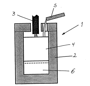
Figure 2 shnWS all ar-C furnace for slag extraction of boron froln Illoltell
SI11C(lrl llSed in
carrying out the method of the present invention.
In Figure 2 there is shown an arc furnace 1 comprising a graphite crucible 2
having a
volume of 50 drn-~ equipped with an electrode 3 for melting silicon 4 and slag
materials.
The furnace 1 is further equipped with means 5 for continuously supply of slag
to the
2f) furnace and means for removal of the slag (not shown). The furnace has a
maximum
load of 70 kW . In order to inactivate the slag the furnace has a rather poor
heat
insulation at the bottom.
EXAMPLE 1 (Present invention)
2~ kilogram of silicon containing 40 ppmw boron was melted in the furnace 1.
40
kilogram of a low boron slag having a composition of CO % by weight Ca0 and 40
~lo by
weight Si02 was added continuously to the silicon through the slag supply
means 5,
while heat was added at a rate that gave almost instanteneous melting. Tlre
melting was
verified by probing into the furnace. The density of the slag was higher than
the density
of silicon thus causing the slag to settle in a slag layer ti below the
silicon layer in the
furnace. After fllllshlllg the slag addition, the refined sIIICOn was tapped
from tile furnace
1. T'Ire mean load during the test was 58.5 KW.
The boron content of the refined silicon was approximately 1 ppmw and as can
he seen
from Figure 1, this is very close to the theoretical value obtainable for the
method
according to the present invention.
7
EXAMPLE 2 (Prior art) 21 5 3 9 3 2
For comparison purposes a test was made where 40 kilogram of slag having the
same
composition as in example 1 was melted in the furnace 1 whereafter 20 kilogram
of
silicon containing 40 ppmw boron was added continuously to the molten slag,
while the
charge was heated at a rate that gave almost instanteneous melting. The two
melts were
kept in contact for about half an hour after completed melting, whereafter the
silicon was
tapped from the furnace. The boron content of the silicon was 11 ppmw) which
is slightly
above the theoretical value of the prior art process shown in Figure 1. The
mean load
during the test was 65.7 KW.
This comparison example shows a high degree of equilibration between the
silicon and
the bottom slag, which indicates a weak inactivation of the slag. Since the
cooling
through the bottom lining is fearly constant, the load gives an indication of
the cooling
which will take place in the bottom slag layer. The test was repeated with a
lower load of
53.4 KW. The boron content of silicon then became 20 ppmw, which is much
higher than
the theoretical value of prior art in Figure 1.
Example 1 compared with Example 2 show that the process of the present
invention gives
a strongly increased boron removal compared to the process according to the
state of art.