Language selection

Search

Patent 2154291 Summary

Third-party information liability

Some of the information on this Web page has been provided by external sources. The Government of Canada is not responsible for the accuracy, reliability or currency of the information supplied by external sources. Users wishing to rely upon this information should consult directly with the source of the information. Content provided by external sources is not subject to official languages, privacy and accessibility requirements.

Claims and Abstract availability

Any discrepancies in the text and image of the Claims and Abstract are due to differing posting times. Text of the Claims and Abstract are posted:

  • At the time the application is open to public inspection;
  • At the time of issue of the patent (grant).
(12) Patent: (11) CA 2154291
(54) English Title: RELAY CONTROL CIRCUIT AND METHOD FOR CONTROLLING A RELAY
(54) French Title: CIRCUIT DE COMMANDE DE RELAIS ET METHODE CONNEXE
Status: Expired
Bibliographic Data
(51) International Patent Classification (IPC):
  • H01H 47/32 (2006.01)
  • H05B 47/10 (2020.01)
(72) Inventors :
  • KNOBLE, DAVID W. (United States of America)
  • JAMASBI, KHOSROW (United States of America)
  • OLSON, JAMES V. (United States of America)
(73) Owners :
  • GENLYTE THOMAS GROUP LLC (United States of America)
(71) Applicants :
  • THOMAS LIGHTING (United States of America)
(74) Agent: SMART & BIGGAR LLP
(74) Associate agent:
(45) Issued: 2007-07-17
(22) Filed Date: 1995-07-18
(41) Open to Public Inspection: 1996-11-02
Examination requested: 2001-07-05
Availability of licence: N/A
(25) Language of filing: English

Patent Cooperation Treaty (PCT): No

(30) Application Priority Data:
Application No. Country/Territory Date
08/432,266 United States of America 1995-05-01

Abstracts

English Abstract

A control relay circuit and method for controlling a relay having a coil, for use, in particular, in operation of a light fixture circuit having an HID lamp. The relay control circuit has an input for receiving a control voltage signal and a voltage storage element connected across the input. The voltage storage element develops a voltage level as a function of time in response to the control voltage signal. A thyristor circuit, a switching element and the coil of the relay form a series circuit that is connected in parallel to voltage storage element. A switch controller is connected in parallel to the voltage storage element and is also connected to the switching element. In response to the control voltage being received at said input, the switch controller activates the switching element to a conductive state at a first voltage level across the voltage storage element and the thyristor changes from a non-conductive state to a conductive state at a second voltage level across the voltage storage element, the first voltage level being less than the second voltage level. In response to the control voltage being removed from the input, the switch controller activates the switching element to a non-conductive state at a third voltage level across the voltage storage element thereby changing the thyristor from the conductive state to the non-conductive state thereof, the third voltage level being less than the second voltage level. The relay is energized at the second voltage level and is deenergized at the third voltage level.


French Abstract

Un circuit de commande de relais et les méthodes de commande d'un relais qui comporte une bobine pour une utilisation, en particulier, dans le fonctionnement d'un circuit de luminaire doté d'une lampe DHI. Le circuit de commande de relais comprend une entrée pour recevoir un signal de tension de commande et un élément de stockage de tension raccordé à l'entrée. L'élément de stockage de tension développe un niveau de tension en fonction du temps de réponse du signal de tension de commande. Un circuit de thyristor, un élément commutateur et la bobine du relais forment un circuit série qui est raccordé en parallèle à l'élément de stockage de tension. Une commande de commutation est raccordée en parallèle à l'élément de stockage de tension et également raccordée à l'élément de commutation. En réaction à la tension de commande reçue à ladite entrée, la commande de commutation active l'élément commutateur à un état conducteur d'un premier niveau de tension dans l'élément de stockage de tension et le thyristor passe d'un état non-conducteur à un état conducteur à un deuxième niveau de tension dans l'élément de stockage de tension, le premier niveau de tension étant inférieur au deuxième niveau de tension. En réaction à la tension de commande coupée à ladite entrée, la commande de commutation active l'élément commutateur à un état non-conducteur d'un troisième niveau de tension dans l'élément de stockage de tension et le thyristor passe d'un état conducteur à un état non-conducteur, le troisième niveau de tension étant inférieur au deuxième niveau de tension. Le relais est sous tension au deuxième niveau de tension et hors tension au troisième niveau de tension.

Claims

Note: Claims are shown in the official language in which they were submitted.


8
CLAIMS:

1. A relay control circuit for controlling a relay
having a coil, comprising:

an input for receiving a control voltage signal
between first and second input terminals;

a voltage storage element connected across said
input, said voltage storage element developing a voltage
level as a function of time in response to said control
voltage signal;

a thyristor circuit, a switching element and the
coil of the relay forming a series circuit that is connected
in parallel to said voltage storage element;

a switch controller connected in parallel to said
voltage storage element and also connected to said switching
element;

responsive to said control voltage signal being
received at said input, said switch controller activating
said switching element to a conductive state at a first
voltage level across said voltage storage element and said
thyristor changing from a non-conductive state to the
conductive state at a second voltage level across said
voltage storage element, said first voltage level being less
than said second voltage level;

responsive to said control voltage signal being
removed from said input, said switch controller activating
said switching element to the non-conductive state at a
third voltage level across said voltage storage element
thereby changing said thyristor from the conductive state to


9
the non-conductive state thereof, said third voltage level
being less than said second voltage level; and

wherein said relay is energized at said second
voltage level and is deenergized at said third voltage
level.

2. The relay control circuit according to claim 1,
wherein said relay has at least one set of normally-closed
contacts, and wherein when said control voltage signal is
removed from said input and when the voltage level across
the voltage storage element reduces to said third voltage
level, said switching element causes said relay to release
with zero current through said coil resulting in a

predetermined closure force of said at least one set of
normally-closed contacts.

3. The relay control circuit according to claim 1,
wherein said voltage storage element is a capacitor.

4. The relay control circuit according to claim 1,
wherein said thyristor circuit has; a first transistor with
an emitter-collector path connected between the coil and an
input terminal of the input, a second transistor with a
collector-emitter path connected between the coil and the
input terminal, a base of the first transistor connected to
the collector of the second transistor and a base of the
second transistor connected to the collector of the first
transistor, and a zener diode connected from the base of the
second transistor to the base of the first transistor.

5. The relay control circuit according to claim 1,
wherein said switch controller has; a series circuit having
first and second resistors and a zener diode connected in


parallel to said voltage storage element, and a switching
transistor having a collector-emitter path connected between
the thyristor circuit and the second input terminal and a
base connected to a juncture of said first and second
resistors.


6. A method for controlling a relay having a coil,
comprising:

providing a control voltage signal to an input
between first and second input terminals;

providing a voltage storage element connected
across said input, said voltage storage element developing a
voltage level as a function of time in response to said
control voltage signal;

providing a series circuit having a thyristor
circuit, a switching element and the coil of the relay, the
series circuit being connected in parallel to said voltage
storage element;

providing a switch controller connected in
parallel to said voltage storage element and also connected
to said switching element;

activating via said switch controller, in response
to said control voltage signal being received at said input,
said switching element to a conductive state at a first
voltage level across said voltage storage element and said
thyristor changing from a non-conductive state to the
conductive state at a second voltage level across said
voltage storage element, said first voltage level being less
than said second voltage level;


11

activating via said switch controller, in response
to said control voltage signal being removed from said
input, said switching element to the non-conductive state at
a third voltage level across said voltage storage element
thereby changing said thyristor from the conductive state to
the non-conductive state thereof, said third voltage level
being less than said second voltage level; and

wherein said relay is energized at said second
voltage level and is deenergized at said third voltage
level.


7. The method according to claim 6, wherein said
relay has at least one set of normally-closed contacts, and
wherein when said control voltage signal is removed from
said input and when the voltage level across the voltage
storage element reduces to said third voltage level, said
switching element causes said relay to release with
substantially zero current through said coil resulting in a
predetermined closure force of said at least one set of
normally-closed contacts.


8. The method according to claim 6, wherein said
voltage storage element is a capacitor.


9. The method according to claim 6, wherein said
thyristor circuit has; a first transistor with an emitter-
collector path connected between the coil and the second
input terminal, a second transistor with a collector-emitter
path connected between the coil and the second input
terminal, a base of the first transistor connected to the
collector of the second transistor and a base of the second
transistor connected to the collector of the first


12
transistor, and a zener diode connected from the base of the
second transistor to the base of the first transistor.

10. The method according to claim 6, wherein said
switch controller has; a series circuit having first and
second resistors and a zener diode connected in parallel to
said voltage storage element, and a switching transistor
having a collector-emitter path connected between the
thyristor circuit and the second input terminal and a base
connected to a juncture of said first and second resistors.
11. A light control system for changing light
intensity levels of a lamp, comprising:

a light fixture circuit connected to said lamp,
said light fixture circuit operating said lamp at a first
intensity level at a first circuit setting and at a second
intensity level at second circuit setting, said light

fixture circuit having first and second input terminals
connected to setting circuitry for forming said first and
second circuit settings;

a relay control circuit having a relay, said relay
having a coil and at least one set of normally-closed
contacts, said at least one set of normally-closed contacts
connected to first and second output terminals of said relay
control circuit, said first and second output terminals of
said relay control circuit operatively connected to said
first and second input terminals of said light fixture
circuit, respectively;

said relay control circuit having first and second
input terminals for receiving a control voltage signal;

said relay control circuit having a voltage
storage element connected across said first and second input


13
terminals of said relay control circuit, said voltage
storage element developing a voltage level as a function of
time in response to said control voltage signal;

said relay control circuit having a thyristor
circuit, a switching element and the coil of the relay
forming a series circuit that is connected in parallel to
said voltage storage element;

said relay control circuit having a switch
controller connected in parallel to said voltage storage
element and also connected to said switching element;

responsive to said control voltage signal being
received at said first and second input terminals of said
relay control circuit, said switch controller activating
said switching element to a conductive state at a first
voltage level across said voltage storage element and said
thyristor changing from a non-conductive state to the
conductive state at a second voltage level across said
voltage storage element, said first voltage level being less
than said second voltage level;

responsive to said control voltage signal being
removed from said first and second input terminals of said
relay control circuit, said switch controller activating
said switching element to the non-conductive state at a
third voltage level across said voltage storage element
thereby changing said thyristor from the conductive state to
the non-conductive state thereof, said third voltage level
being less than said second voltage level; and

wherein said relay is energized at said second
voltage level whereby said light fixture circuit forms said
first setting and said lamp is operated at said


14
first intensity level, and wherein said relay is deenergized at
said third voltage level whereby said light fixture circuit
forms said second setting and said lamp is operated at said
second intensity level.

12. The light control system according to claim 11,
wherein when said control voltage signal is removed from said
first and second input terminals of said relay control circuit
and when the voltage level across the voltage storage element
reduces to said third voltage level, said switching element
causes said relay to release with zero current through said coil
resulting in a predetermined closure force of said normally-
closed contacts.

13. The light control system according to claim 11,
wherein said voltage storage element is a capacitor.

14. The light control system according to claim 11,
wherein said thyristor circuit has; a first transistor with an
emitter-collector path connected between the coil and the second
input terminal, a second transistor with a collector-emitter
path connected between the coil and the second input terminal of
the relay control circuit, a base of the first transistor
connected to the collector of the second transistor and a base
of the second transistor connected to the collector of the first
transistor, and a zener diode connected from the base of the
second transistor to the base of the first transistor.


-15-
15. The light control system according to claim 11,
wherein said switch controller has; a series circuit
having first and second resistors and a zener diode
connected in parallel to said voltage storage element,
and a switching transistor having a collector-emitter
path connected between the thyristor circuit and the
second input terminal of the relay control circuit and
a base connected to a juncture of said first and second
resistors.

Description

Note: Descriptions are shown in the official language in which they were submitted.


CA 02154291 2005-07-29
72451-32

-1-
~tELAY CONTROI, CIRCUIT AND METHOD FOR -
CONTROLLING A RELAY
BACKGRbUND OF THE 7NVENTIQN
The present invention relates in general to a relay
control cixouit for controlling a relay and, in
particular, a relay control circuit for controlling a
light fixture circuit.
In the prior art, HID lamps are operated between
a high or full intensity light level and a dim or reduced
light intensity level in response to a control signal.
The change of intensity level of the light output of the
HID lamp is effected by changing a capacitance value in
the light fixture circuit. This is accomplished by
connecting and disconnecting a first capacitor across a
second capacitor by means of relay contacts. Although
the prior art systems provided good operation for
switching the HID lamp between high and low light output
settings, it has baen found that when the relay has
normally- closed contacts, the useful life of the relay
is limited. The drawback of such a controller circuit
is in the deactivation of the relay. The prior art
controller circuit that controls operation of the relay
produces a gradually decreasing current flow through the
coil of the relay. As a result, the speed with which the
rocker of the relay opens is slower than if the current
were suddenly switch'ed to zero through the coil. This
places less force on closing the normally-ciosed contacts
than is desirable. This lower contact force causes the
contacts to degrade more rapidly, eventually failing by
welding together.


CA 02154291 2005-07-29
72451-32

-2-
This drawback will become more evident on
considering in detail Figure 1.

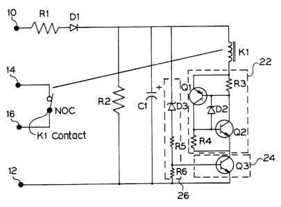
Figure 1 depicts a prior art controlle.r in which
input. terminal 10 is connected to input terminal 12 via the
sex'ies circuit of resistor R1, diode Dl and resistor R2. A
storage capacitor Cl is connected across resistor R2. Also,
connected across resistor R2 is a series circuit composed of
the coil of relay K1, and a thyristor circuit 22. The
thyristor circuit 22 is formed by transistors Q1 and Q2 with
resistors R3 and R4 and diode D2 as depicted in FIG. 1.
Normally-opened contacts NOC of the relay Kl are connected
across output terminals 14 and 16 of the controller.

Operation of this prior art, controller depicted in
FIG. 1 is as follows. When approximately 120 volts AC is
applied between terminals 10 and 12, the capacitor Cl
charges. Transistors Q1 and Q2, and the supporting
circuitry of resistors R3 and R4 and diode D2 form the
effective thyristor circuit 22. When a voltage is placed
across this thyristor circuit 22, the transistors Qi and Q2
will remain in the off-state until the voltage exceeds a
threshold determined by diode 02. When this threshold is
exceeded, current flows through the circuit with transistors
Ql and Q2 now in a conductive state, until the voltage
across the circuit is reduced to zero volts. Therefore,
when capacitor Cl charges up to an appropriate voltage
(about 50 volts), transistors Ql and 02 turn-on, pexrnitting
cur3-ent to flow through the relay coil of relay Kl. It is a
property of relays that they need a higher voltage to
activate then to maintain. That is, it takes a higher
voltage to close the rocker of the relay magnetically, than
'to keep the rocker closed. Furthermore, the use of the
circuit permits lower current to be used, lessening power
consumption, resistor temperatures, etc.


CA 02154291 2005-07-29
72451-32

-3-
The drawback of this prior art circuit depicted in
FIG. ]. is in the deactivation of the relay. This drawback
was, identified during light tests, in which the normally-
closed contacts of the relay did not exhibit sufficiently
long life. When the control voltage is removed from
terminals 10 and 12, the capacitior Cl gradually discharges
through the coil of relay Kl_ At some point in time, the
current is sufficiently low in that the rocker of relay Kl
opens. However, due t.o the current still flowing through
the cail of relay K1, the speed with which the rocker opens
is less than desired. As previously mentioned this places
less force in closing the normally-closed contacts of the
relay K1, than is desirab].e. This lower contact force will
eventually destroy the contacts of the relay Kl.

The present invention overcomes these drawbacks in
ths prior art controller.

SUMMALtY OF THE INVENTION

It is an object of the present invention to
provide an improved relay control circuit for controlling a
rolay, in particular, a relay used to operate an HID lamp.

In general terms, the present invention is a relay
control circuit and method for controlling the relay, the
relay having a coil and at least one set of normally closed
con'tacts. The relay control circuit has an input for
reciaiving a control voltage signal and a voltage storage
element connected across the input. The voltage storage
eleinent develops avoltage level as a function of time in
response to the control voltage signal. A thyristor
circuit, a switching element and the coil of the zelay form
a seeries circuit that is connected in parallel to voltage
storage element. A switch contxoller is connected in
parallel to the voltage storage element and is also


CA 02154291 2006-07-26
72451-32

4
connected to the switching element. In response to the
control voltage being received at said input, the switch
controller activates the switching element to a conductive
state at a first voltage level across the voltage storage

element and the thyristor changes from a non-conductive
state to a conductive state at a second voltage level across
the voltage storage element, the first voltage level being
less than the second voltage level. In response to the
control voltage being removed from the input, the switch

controller activates the switching element to a non-
conductive state at a third voltage level across the voltage
storage element thereby changing the thyristor from the
conductive state to the non-conductive state thereof, the
third voltage level being less than the second voltage

level. The relay is energized at the second voltage level
and is deenergized at the third voltage level.

According to an aspect of the invention, there is
provided a relay control circuit for controlling a relay
having a coil, comprising: an input for receiving a control

voltage signal between first and second input terminals; a
voltage storage element connected across said input, said
voltage storage element developing a voltage level as a
function of time in response to said control voltage signal;
a thyristor circuit, a switching element and the coil of the
relay forming a series circuit that is connected in parallel
to said voltage storage element; a switch controller
connected in parallel to said voltage storage element and
also connected to said switching element; responsive to said
control voltage signal being received at said input, said

switch controller activating said switching element to a


CA 02154291 2006-07-26
72451-32

-4a-
conductive state at a first voltage level across said
voltage storage element and said thyristor changing from a
non-conductive state to the conductive state at a second
voltage level across said voltage storage element, said

first voltage level being less than said second voltage
level; responsive to said control voltage signal being
removed from said input, said switch controller activating
said switching element to the non-conductive state at a
third voltage level across said voltage storage element

thereby changing said thyristor from the conductive state to
the non-conductive state thereof, said third voltage level
being less than said second voltage level; and wherein said
relay is energized at said second voltage level and is

deenergized at said third voltage level.

According to another aspect of the invention,
there is provided a method for controlling a relay having a
coil, comprising: providing a control voltage signal to an
input between first and second input terminals; providing a
voltage storage element connected across said input, said

voltage storage element developing a voltage level as a
function of time in response to said control voltage signal;
providing a series circuit having a thyristor circuit, a
switching element and the coil of the relay, the series
circuit being connected in parallel to said voltage storage

element; providing a switch controller connected in parallel
to said voltage storage element and also connected to said
switching element; activating via said switch controller, in
response to said control voltage signal being received at
said input, said switching element to a conductive state at

a first voltage level across said voltage storage element


CA 02154291 2006-07-26
72451-32

-4b-
and said thyristor changing from a non-conductive state to
the conductive state at a second voltage level across said
voltage storage element, said first voltage level being less
than said second voltage level; activating via said switch

controller, in response to said control voltage signal being
removed from said input, said switching element to the non-
conductive state at a third voltage level across said
voltage storage element thereby changing said thyristor from
the conductive state to the non-conductive state thereof,

said third voltage level being less than said second voltage
level; and wherein said relay is energized at said second
voltage level and is deenergized at said third voltage
level.

According to a further aspect of the invention,
there is provided a light control system for changing light
intensity levels of a lamp, comprising: a light fixture
circuit connected to said lamp, said light fixture circuit
operating said lamp at a first intensity level at a first
circuit setting and at a second intensity level at second

circuit setting, said light fixture circuit having first and
second input terminals connected to setting circuitry for
forming said first and second circuit settings; a relay
control circuit having a relay, said relay having a coil and
at least one set of normally-closed contacts, said at least
one set of normally-closed contacts connected to first and
second output terminals of said relay control circuit, said
first and second output terminals of said relay control
circuit operatively connected to said first and second input
terminals of said light fixture circuit, respectively; said

relay control circuit having first and second input


CA 02154291 2006-07-26
72451-32

-4c-
terminals for receiving a control voltage signal; said relay
control circuit having a voltage storage element connected
across said first and second input terminals of said relay
control circuit, said voltage storage element developing a

voltage level as a function of time in response to said
control voltage signal; said relay control circuit having a
thyristor circuit, a switching element and the coil of the
relay forming a series circuit that is connected in parallel
to said voltage storage element; said relay control circuit

having a switch controller connected in parallel to said
voltage storage element and also connected to said switching
element; responsive to said control voltage signal being
received at said first and second input terminals of said
relay control circuit, said switch controller activating

said switching element to a conductive state at a first
voltage level across said voltage storage element and said
thyristor changing from a non-conductive state to the
conductive state at a second voltage level across said
voltage storage element, said first voltage level being less

than said second voltage level; responsive to said control
voltage signal being removed from said first and second
input terminals of said relay control circuit, said switch
controller activating said switching element to the non-
conductive state at a third voltage level across said
voltage storage element thereby changing said thyristor from
the conductive state to the non-conductive state thereof,
said third voltage level being less than said second voltage
level; and wherein said relay is energized at said second
voltage level whereby said light fixture circuit forms said

first setting and said lamp is operated at said first


CA 02154291 2006-07-26
72451-32

-4d-
intensity level, and wherein said relay is deenergized at
said third voltage level whereby said light fixture circuit
forms said second setting and said lamp is operated at said
second intensity level.

BRIEF DESCRIPTION OF THE DRAWINGS
Features of the present invention which are
believed to be novel are set forth with particularity in the
appended claims. The invention together with further
objects and advantages may best be understood by reference

to the following description, taken in conjunction with the
accompanying drawings, in the several figures of which like
reference numerals identify like elements, and in which:

Figure 1 is a circuit diagram of a prior art
controller for controlling a light fixture circuit;

Figure 2 is a circuit diagram of a light fixture
circuit for use in the present invention;

Figure 3 is a circuit diagram of a relay control
circuit of the present invention for controlling the light
fixture circuit of Figure 2; and


CA 02154291 2005-07-29
72451-32

-5-
Figure 4 is a general block diagram depicting one
embodiment of the present invention.

DESCRIPTION OF THE PREFERRED EMBpuIMENTS

The present invention has general applicability,
but is most advantageously utilized in a system as depicted
in Figure 4. As depicted in Figure 4, a signal source 30 is
connected to a controller 32 which receives a control voltage
signal on terminals 10 and 12 thereof. The controller 32 is
connected to a light fixture circuit 34 that contains, for
example, an HID lamp. The controller 32 has output
terniinals 14 and 16 connected to input terminals 18 and 20,
respectively, of the light fixture circuit 34.

FXG. 2 depicts a typical light fixture circuit for
an HID lamp in which a transformer 40 is connected on one
side to an AC line having a line common 42, 120 volt AC
tap 44, and a 277 volt AC line 46. The other side of the
transformer 40 is connected to the HID lamp 4$ via a first
capacitor 50. A second capacitor 52 is connectable across
the first capacitor 50 by means of the relay contacts of the
rel-ay K1 in the controller 32. The change in capacitance
effected by the connection and disconnection of the second
capacitor 52 across the first capacitor 50, produces the
change in light intensity level of the HID lamp 4a.

The present invention, which overcomes the
drawbacks of the FIG. 1 prior art controller, is depicted in
FIG. 3. The controller of the present invention has a
switch element 24 which is connected in series with the


2154291
-6-

coil of the relay Ki and the thyristor circuit 22. In
particular, the switch element 24 has a transistor Q3
with its collector-emitter path connected between input
terminal 12 and the transistor Q2 of the thyristor
circuit 22. A switch controller 26 has a zener diode D3
in series with resistors R5 and R6. The switch controller
26 is connected across capacitor Cl. The juncture of
resistors R5 and R6 is connected to the base of
transistor Q3 for turning Q3 on and off. The transistor
Q3 is on, or in a conductive state, anytime that the
voltage on capacitor Cl is higher than the characteristic
voltage zener diode D3. When a control voltage is
applied to input terminals 10 and 12, the voltage on
capacitor Cl increases until zener diode D3 conducts.
At this point in time, current flows through resistors
R5 and R6 thereby turning on a transistor Q3. The
voltage on capacitor Cl then continues to increase until
transistors Qi and Q2 turn on, activating the relay K1
as described above. Thus, activation of the relay is
essentially unchanged, since transistor Q3 is always in
a conductive state before transistors Ql and Q2 turn on.
When the control voltage is removed from input
terminals 10 and 12, the following occurs. The voltage
on capacitor Cl decreases as its stored energy is drained
by the coil of relay K1. Each of transistors Q1, Q2 and
Q3 are still in a conductive state. However, when the
voltage on capacitor Cl decreased to a low enough level,
zener diode D3 ceases to conduct, and transistor Q3 turns
off. When transistor Q3 turns off and becomes non-
conductive, current through the coil of relay K1 ceases
to flow, and transistors Q1 and Q2 then also turn off.


Z154291
-7-

Thus, the relay rocker releases with no current flowing
through the coil of relay Kl, and the proper closure
forces are applied to the normally-closed contacts.
Whereas in the prior art controller circuit depicted in
FIG. 1 the rocker of the relay K1 closed slowly due to
the gradually decreasing current flow through the coil
of the relay Ki, in the present invention depicted in
FIG. 3 the current flow through the coil of K1 is
suddenly cut-off, that is dropped to zero, and the rocker
of the relay K1 closes rapidly and prevents damage to the
normally-closed contacts of the relay K1.
The invention is not limited to the particular
details of the method and apparatus depicted and other
modifications and applications are contemplated. Certain
other changes may be made in the above-described
apparatus and method without the parting from the true
spirit and scope of the invention herein involved. It
is intended, therefore, that the subject matter in the
above-depiction shall be interpreted as illustrative and
not in a limiting sense.

Representative Drawing
A single figure which represents the drawing illustrating the invention.
Administrative Status

For a clearer understanding of the status of the application/patent presented on this page, the site Disclaimer , as well as the definitions for Patent , Administrative Status , Maintenance Fee  and Payment History  should be consulted.

Administrative Status

Title Date
Forecasted Issue Date 2007-07-17
(22) Filed 1995-07-18
(41) Open to Public Inspection 1996-11-02
Examination Requested 2001-07-05
(45) Issued 2007-07-17
Expired 2015-07-20

Abandonment History

There is no abandonment history.

Payment History

Fee Type Anniversary Year Due Date Amount Paid Paid Date
Application Fee $0.00 1995-07-18
Registration of a document - section 124 $0.00 1995-10-05
Maintenance Fee - Application - New Act 2 1997-07-18 $100.00 1997-06-04
Maintenance Fee - Application - New Act 3 1998-07-20 $100.00 1998-06-18
Maintenance Fee - Application - New Act 4 1999-07-19 $100.00 1999-06-28
Maintenance Fee - Application - New Act 5 2000-07-18 $150.00 2000-06-23
Maintenance Fee - Application - New Act 6 2001-07-18 $150.00 2001-06-26
Request for Examination $400.00 2001-07-05
Registration of a document - section 124 $100.00 2001-07-16
Maintenance Fee - Application - New Act 7 2002-07-18 $150.00 2002-06-04
Maintenance Fee - Application - New Act 8 2003-07-18 $150.00 2003-07-10
Maintenance Fee - Application - New Act 9 2004-07-19 $200.00 2004-04-21
Maintenance Fee - Application - New Act 10 2005-07-18 $250.00 2005-07-18
Maintenance Fee - Application - New Act 11 2006-07-18 $250.00 2006-07-07
Final Fee $300.00 2007-04-24
Maintenance Fee - Patent - New Act 12 2007-07-18 $250.00 2007-07-06
Maintenance Fee - Patent - New Act 13 2008-07-18 $250.00 2008-07-16
Maintenance Fee - Patent - New Act 14 2009-07-20 $250.00 2009-07-08
Maintenance Fee - Patent - New Act 15 2010-07-19 $450.00 2010-07-07
Maintenance Fee - Patent - New Act 16 2011-07-18 $450.00 2011-07-15
Maintenance Fee - Patent - New Act 17 2012-07-18 $450.00 2012-07-12
Maintenance Fee - Patent - New Act 18 2013-07-18 $450.00 2013-07-16
Maintenance Fee - Patent - New Act 19 2014-07-18 $450.00 2014-07-07
Owners on Record

Note: Records showing the ownership history in alphabetical order.

Current Owners on Record
GENLYTE THOMAS GROUP LLC
Past Owners on Record
JAMASBI, KHOSROW
KNOBLE, DAVID W.
OLSON, JAMES V.
THOMAS LIGHTING
Past Owners that do not appear in the "Owners on Record" listing will appear in other documentation within the application.
Documents

To view selected files, please enter reCAPTCHA code :


To view images, click a link in the Document Description column. To download the documents, select one or more checkboxes in the first column and then click the "Download Selected in PDF format (Zip Archive)" or the "Download Selected as Single PDF" button.

List of published and non-published patent-specific documents on the CPD .

If you have any difficulty accessing content, you can call the Client Service Centre at 1-866-997-1936 or send them an e-mail at CIPO Client Service Centre.


Document
Description 
Date
(yyyy-mm-dd) 
Number of pages   Size of Image (KB) 
Drawings 2001-09-24 2 44
Cover Page 1996-11-21 1 17
Description 1996-11-02 7 286
Claims 1996-11-02 8 288
Abstract 1996-11-02 1 42
Representative Drawing 1998-04-15 1 10
Drawings 1996-11-02 2 35
Claims 2005-07-29 8 275
Description 2005-07-29 7 257
Claims 2006-07-26 8 263
Representative Drawing 2006-11-29 1 9
Description 2006-07-26 11 406
Cover Page 2007-06-27 1 51
Prosecution-Amendment 2001-07-05 1 34
Assignment 1995-07-18 10 456
Prosecution-Amendment 2001-07-05 1 51
Correspondence 1995-08-23 4 124
Prosecution-Amendment 2006-02-23 2 43
Prosecution-Amendment 2005-02-01 2 48
Prosecution-Amendment 2005-07-29 10 315
Fees 2005-07-18 1 34
Prosecution-Amendment 2006-07-26 13 481
Correspondence 2007-04-24 1 38
Fees 2008-07-16 1 35
Correspondence 2009-06-26 4 211
Correspondence 2009-07-06 1 16
Fees 2009-07-08 1 56