Note: Descriptions are shown in the official language in which they were submitted.
~ WO 95/17043 2 1 ~ 4 ~ ~ ~ PCT/US94113339
APPARATUS AND Mh~HOD FOR CO~TR~LL~G T~IE
LOOP BAl~wwlLrl~n OFAP~IASE LOCK~) LOOP
S Fi.ql-l of the Invention
The present invention relates generally to radio commllnication
transceivers and, more particularly, to an apparatus and method for
controlling the loop bandwidth of a phase locked loop.
1 0
Rackgrolmd of t.h~ Invention
FIG. 1 illustrates, by e~mple, a block diagram of a conventional
radio commllnic~tio~ transceiver 100 (hereinafter lefe.led to as
"transceivel"). The transceiver 100 en~bles a mobile or portable
subscriber unit to communicate with a base station (not shown), for
example, over radio frequency (RF) ~h~nnel~ in a radio communication
system (not shown). The base station thereafter provides
commllnic~tions with a l~nrlline telephone system (not shown) and
2 0 other subscriber units. An e~mple of a subscriber unit having the
transceiver 100 is a cell~ r radiotelephone.
The transceiver 100 of FIG. 1 generally in~ es an ~nte~n~ 101, a
duplex filter 102, a receiver 103, a transmitter 105, a lefelellce frequency
signal source 107, a receive (Rx) phase locked loop (PLL)frequency
2 5 synt.he~i7.er 108, a tr~n.~rr.it (Tx) PLL frequency synt.hesi7er 109, a
processor 110, an information source 106, and an information sink 104.
The illteIconnection of the blocks of the transceiver 100 and
operation thereof is ~l~scribed as follows. The ~ntenn~ 101 receives a RF
signal 119 from the base station for filtering by the ~ pl~.~ filter 102 to
3 0 produce an RF received signal at line 111. The tlnple~r filter 102 provides
frequency selectivity to separate the RF received signal at line 111 and
the RF transmit signal at line 113. The receiver 103 is coupled to receive
the RF received signal at line 111 and operative to produce a received
baseband signal at line 112 for the information sink 104. The RF signal
3 S source 107 provides a ~efe~ ce frequency signal at line 115. The Rx PLL
frequency syn~e~i~er lQ8 is coupled to receive the RF signal at line 115
and inform~tio~ on a data bus 118 and operative to produce a receiver
WO 95/17043 1 '- PCTIUS94/13339 ~
215~8~
- 2 -
tune signal at line 116 to tune the receiver 103 to a particular RF
çh~nnel Likewise, the Tx PLL frequency synt.hesi~er 109 is coupled to
receive the RF signal at line 116 and information on the data bus 118 and
operative to produce a transceiver tune signal at line 117 to tune the
S transmitter 105 to a particular RF r.h~nn~l. The processor 110 controls
the operation of the Rx PLL frequency synt~.ci7.er 108, the Tx PLL
frequency synt.he~ei7er 109, the receiver 103, and the tr~nemitter 10~ via
the data bus 118. The information source 106 produces a baseband
transmit signal at line 114. The transmitter 10~ is coupled to receive the
1 0 baseband transmit signal at line 114 and ope,ative to produce the RF
transmit signal at line 113. The duplex filter 102 filters the RF transmit
signal at line 113 for r~ tion by the ~nt~enn~ 101 as a RF signal 120.
The RF çh~nn~le in a cellular radiotelephone system, for
~mple, include voice and fii~n~ling rh~nnele for transmitting and
l S receiving (hereinafter referred to as "transceiving") inform~tio~
between the base station and the subscriber units. The voice rh~nnel.
are allocated for transceiving voice information. The fiign~ling
f~h~nnel.e, also ~arel-l2d to as control r.h~nnele~ are allocated for
transceiving data and eiFn~lin~ inform~t.io~. It is through these
2 0 eign~lin~ ch~nnçlc that the subscriber units gain access to the cellular
radiotelephone system and are ~e.$igne-l a voice r.h~nnel for further
commllnic~tion with the l~n-llin~ telephone system. In celllll~r
radiotelephone ~y~Lellls capable of transceiving wideband data on the
~ign~lin~ ch~nnele, the frequency spacing of the ,eign~ling rhs~nn~l.e
2 S may be a multiple of the frequency spacing of the voice r.h~nnel~
In some celllll~r radiotelephone systems, the transceiver 100 and
the base station intermittently transceive information therebetween on
the .cign~ling ch~nne.l. One such ~y~Lelll, for example, uses a time
division multiple access (TDMA) sign~lin~ method to synchronize the
3 0 intermittent illfo~ ation. In this ty-pe of :iy~Lt~ , keeping the transceiver
100 fully powered during the entire time that the transceiver 100 is tuned
to the .eign~lin~ ch~nnel llnnacesfi~rily drains the transceiver's battery
during those times when the information is not received. TheIefole,
portions of the transceiver 100 can be powered off to prolong battery life
3 5 when the transceiver is not transceiving inform~qt.io~- Further, portions
of the transceiver 100 can be powered offto prolong battery life when the
WO 95117043 21 ~ 9 PCT/US94/13339
signal quality is good enough such that further repetition of the same
information is not needed. Intermittently powering on and off, i.e.
en~hling and rli.~,qhling, the transceiver 100 during its receive operation
is called discontinuous receive (DRX) mode of operation. In the DRX
S mode of operation, quickly en~hling and tli~hling the portions of the
transceiver 100 produces the greatest savings in battery life.
FIG. 2 illustrates, by e~mple, a block diagram of a conventional
phase locked loop (PLL) frequency synt.hesi7.er for use in the transceiver
100 of FIG. 1. The general structure of the PLL frequency synt.he.ci7çr of
1 0 FIG. 2 is the same for both the Rx PLL frequency synthe.~i7er 108 and the
Tx PLL frequency synthesi7.er 109.
The PLL frequency synt.h~i7er 108 or 109 of Fig. 2 generally
inrllllles a la~elellce divider 201, for discussion purposes, and a PLL 212.
The PLL 212 generally inrlll~le~ a phase detector 202, a loop filter 203, a
1 5 voltage controlled oscill~tor 204, and a loop divider 205. The lafel~--ce
divider 201 receives a reference frequency signal on line 115.
The intercoTlnection of the blocks of the PLL frequency synthe.~i7~r
108 or 109 is described as follows. The phase detector 202 is coupled to
receive a divided lafele,lce frequency signal at line 206 and a feedback
2 0 signal at line 209, and opelative to produce a phase error signal at line
207. The loop filter 203 is coupled to receive the phase error signal 207,
and opeldlive to produce a filtered signal at line 208. The voltage
controlled osrill~tor 204 is coupled to receive the filtered signal at line 208
and opeldtive to produce an oul~ul frequency signal at line 116 or 117.
2 5 The loop divider 205 is coupled to receive the oul~ul, frequency signal at
line 116 or 117, and opelative to produce the fee~lh~r.k signal at line 209.
The loop divider 205 and the reference divider 201 laceives progr~mmin~
information via the data bus 118.
The operation of the PLL frequency synt.he.~i7er 108 or 109 is
3 0 described as follows. The PLL 212 is a circuit which produces the oul~ul
frequency signal at line 116 or 117 synchronized to the larelallce
frequency signal at line 115. The output frequency signal at line 116 or
, 117is synchronized or "locked" to the reference frequency signal at line
115 when the frequency of the output frequency signal at line 116 or 117
3 5 has a predetermined frequency rel~tion~hip to the frequency of the
lefelellce frequency signal at line 115. Under locked conditions, the 212
WO 95/17043 PCT/US94/13339
21~ 448 9 - i .
PLL typically provide a constant phase Lrr~. a~lce between the reference
frequency signal at line 115 and the output frequency signal at line 116 or
117. The constant phase di~ellce may assume any desired value
including zero. Should a deviation in the desired phase difrelellce of
such .cign~lc develop, i.e., should a phase error at line 207 develop due
to, e.g., variation in either the frequency of the reference frequency
signal at line 115 or progr~mm~hle parameters of the PLL via the data
bus 118, the PLLwill ~ttempt to adjust the frequency of the output
frequency signal at line 116 or 117 to drive the phase error at line 207
l 0 toward zero.
The PLL frequency synthe,ci~er 108 or 109 may be rl~Rsified as
belo~gin~ to one of at least two categories based on the predetermined
frequency rel~tioI chip of the output signal frequency at line 116 or 117 to
the frequency of the reference frequency signal at line 115. The first
l 5 category is ~ c~cified as an "integer division" PLL frequency sr~esi7~erwherein the rel~tion.chip between the output frequency signal at line 116
or 117 and . efer~llce frequency signal at line 115 is an integer. The
second category is ~ c~cifie(l as a "fractional division" PLL frequency
synthe~ er in which the relationship between the ou~u~ frequency
2 0 signal at line 116 or 117 and lafe~ ~nce frequency signal at line 115 is a
rational, non-integer number, consisting of an integer and a fraction.
PLL's are characterized by a loop bandwidth. For some
applic~tinns it is desirable to vary the loop bandwidth of the PLL under
certain conditions such as, for example, when the frequency of the
2 5 reference frequency signal at line 116 changes or when the
progr~mm~hle parameters of the PLL via the data bus 118 changes.
Appropriately varying the loop bandwidth advantageously provides
shorter lof~ktir~e, improved noise, and lower spurious si~n~
A problem with varying the loop bandwidth of the PLL 212
3 0 in~ lçs determinin~ when to vary the loop bandwidth. Determining
when to vary the loop bandwidth directly affects the time required for the
PLL 212 to reach a desirable locked condition. It is generally desirable
for the PLL 212 to reach its locked condition quickly~ If the locked
condition of the PLL 212 is not re~rh~rl quickly, noise may be generated
3 5 or information may be lost.
~ WO 95/17043 2 1 5 ~ ~ 8 9 PCT/US94/13339
One prior art solution for determinin~ when to vary the loop
bandwidth of the PLL 212 is to vary the loop bandwidth at a
predetermined time. The disadvantage with this approach is that the
predetermined time does not always correspond to the optimal time
S required for the PLL 212 to reach its desired lock condition because the
predetermined time is not related to the state of the PLL 212.
Another prior art solution for determininE when to vary the loop
bandwidth of the PLL 212 is to vary the loop bandwidth based on an
inst~nt~neous phase error at line 207. The disadvantage with this
1 0 approach is that the ins~nt~neous phase error at line 207 does not fully describe the state of the PLL 212 for all times.
Accordingly, there is a need for an improved apparatus and
method for controlling the loop bandwidth of a PLL advantageously
providing an accurate determin~tion of when to vary the loop bandwidth
1 5 of the PLL.
Rrief nescri~Dtion of th-? r)r~win~
FIG. 1 illustrates a block diagram of a conventio~l radio
2 0 communication transceiver.
FIG. 2 illustrates a block diagram of a conventional phase locked
loop frequency synthe~i7er for use in the radio commllnics~t
transceiver of FIG. 1.
FIG. 3 illustrates a block diagram of a phase locked loop in
2 5 accordance with the present invention.
FIG. 4 is a timing diagram illustrating digital .cign~lc in a loop
bandwidth controller of the phase locked loop of FIG. 3 in accordance
with the present invention.
FIG. ~ illustrates graphs depicting a relationship between the
3 0 value of a counter of the phase locked loop of FIG. 3 and the value of the
loop bandwidth of the phase locked loop of FIG. 3 in accordance with the
present inventior~
FIG. 6 illustrates a flow chart i~s-~rihing steps for controlling the
loop bandwidth of the phase locked loop of FIG. 3 in accordance with the
3 5 present invention.
W O 95/17043 PCTrUS94/13339 ~
2~ 5~89 6 -
net~ilp~l nesrri~tion of ~ Prere~el1 ~mhofliment
In accordance with the present i~lvç~ ;or~ the foregoing need is
subst~nt,i~lly met by improved apparatus and method for controlling the
loop bandwidth of a PLL. Acco~lg to the present invention, the
apparatus and method iflent.ifie.c a phase error, in~lic~t.ive of a difference
between the phase of the reference frequency signal and the phase of an
output frequency .sign~l, of the PLL as either desirable or lln~esirable.
When the apparatus and method i~lent.ifies the phase error as desirable,
1 0 the apparatus and method determines a rate of change of the phase
error over a first predetermined time period to provide an in~ic~t.ion of
frequency error between the frequency of the reference frequency signal
and the frequency of the output frequency signal; and controls a
transition between a first and a second loop bandwidth state of the PLL
1 5 responsive to the in~lic~t.ion of the frequency error. When the apparatus
and method itlent.ifies the phase error as llntle~irable, the PLL operates
in the second loop bandwidth state. The present invention
advantageously provides an accurate deter~nin~tion of when to vary the
loop bandwidth of the PLL.
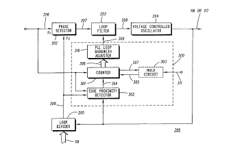
2 0 The present illvelllion can be more fully described with ~efeIe~lceto FIGs. 3-6, wherein FIG. 3 illustrates a block diagram of a phase
locked loop 308 in accordance with the present invention The PLL 308
has the same structure and operates in the same m~nner as the prior
art PLL 212 with the exception of a novel apparatus 300 and the
2 5 associated method therefor. The~efole, in the ~efe~-~ed embo~iment of
the present invent.io~, the novel PLL 308 is substituted for the prior art
PLL 212 for use in the R~ PLL ~requency srthe~i~er 108 or in the Tx PLL
frequency synthesi~er 109 in the transceiver 100. One of ordinary skill in
the art of PLL design and applic~tio~ may find other applic~tions for the
3 0 novel PLL 308 both inside and outside the radio commlmic~tions field.
The novel PLL circuit 308 generally in~ 1es a phase detector 202,
a loop filter 203, a voltage controlled oscill~tor (VCO) 204, a loop divider
205, and a loop bandwidth controller 300. Individually, the phase
detector 202, the loop filter 203, the VCO 204, and the loop divider 20~ are
3 5 generally well known in the art; thus, no filrther discussion will be
presented except to facilitate the underst~n~lin~ of the present inventi
~ wo9S/l7043 21~ 9 PCT/US94113339
A novel loop bandwidth controlser 300 wisl be described and illustrated
below with reference to FIGs. 3-6, in accordance with the present
invention.
The novel PLL 308, with the e~ce~lion of the novel loop bandwidth
S controller 300, may be implemented, for e~mple, using a Motorola
MC145170 PLL frequency synt~le.ci~er and a Motorola MC1648 voltage
controlled os~ tor. The loop filter 205 may be implemerlted, for
example, with standard resistors and capacitors in accordance with
well known filter design techniques.
1 0 Generally, the novel PLL 308 operates as follows. The novel PLL
308 generates an ouL~uL frequency signal responsive to a reference
frequency .~i~n~l The oul~uL frequency signal and the reference
frequency signal are each characterized by frequency and phase. A
phase error is in~ic~tive of the di~lellce between the phase of the
1 5 lefelellce frequency signal and the phase of the o sL~ut frequency sign~l
The PLL opelative in a first loop bandwidth state to m~int~in the ouL~ut
frequency signal subst~nti~lly at a frequency in(lic~tive of the reference
frequency ~ign~l, and opelati~,e in a second loop bandwidth state to
coSlveS~e the o~ uL frequency signal to the frequency intlic~tive of the
lefe~ellce frequency sign~l
The iSlte~. ollnections between the novel loop bandwidth controller
300 and the conventior ~l PLL loop 212 to form the novel PLL 308 are as .
follows. The loop bandwidth controller 300 is coupled to receive the
divided lereS~llce frequency signal at line 206, the feedback signalS at line
2 5 209, and the oul~uL frequency signal at line ~ 16 or 117. The novel loopbandwidth controller 300 produces a loop bandwidth adjust signal at line
309 that is coupled to the loop filter 203.
The loop bandwidth controller 300 further comprises an edge-
5Jsvxis~sity detector 302, a couslLer 301, a PLL loop bandwidth adjuster 310,
3 0 and an optional hold circuit 303. Individualsly, the edge-proximity
detector 302, the couSlter 301, the PLL loop bandwidth adjuster 310 and
the optional hold circuit 303 are well known in the art; hence, no
additionas description need be provided here except as may be nÇcçss:lry
to facilitate the underst~n-ling of the present invention- The
3 S comhin~tion of the edge-proximity detector 302, the counter 301, the PLLloop bandwidth adjuster 310, and the optional latch circuit 303 as used in
WO95tl7W3 PCT~S94/13339
2 1 ~ 8-
the novel PLL 308 of FIG. 3 is considered to be novel and will be described
in further detail below.
.~ .
The edge~ imity detector 302 and the hold circuit 303 may be
implemented, for example, using standard logic elemerltc. Such logic
S element~ may include, for e~mple, NAND gates as a Motorola
MC74HC00, NOR gates such as MC74HC02, and D-type flip-flops such as
MC74HC74 in accordance with well known logic design terhniques. The
counter 301, may be implemented, for ~ mple, using a conventional
counter such as a Motorola MC74HC173. The PLL loop bandwidth
1 0 adjuster 310 may be impleInente-l with standard resistors and
capacitors and using standard ~n~log multiplexers such as Motorola's
MC74HC4066 in accordance with well known design te~hniques.
The i~ltelco~lnections between the blocks of the novel loop
bandwidth controller 300 are as follows. The edge-~lo,~ y detector 302
l 5 is coupled to receive the divided lefele~lce frequency signal at line 206
and the fee~h~c~k signal at line 209, and operative to produce a counter
reset signal at line 304. The counter 301 is coupled to receive the divided
reference frequency signal at line 206 and the counter reset signal at line
304, and operative to produce a count value at line 306 and an in~lic~ti
2 0 of the count value at line 307. The optional hold circuit 303 is coupled to
receive indication of the count value at line 307 and a hold enable signal
at line 311 produced by the processor 110, and opela~ive to produce a hold
signal at line 30~ for the counter 301.
The operation of the novel loop bandwidth controller 300iS as
2 5 follows. According to the present invention, the edge ~lo~ ity detector
and associated method therefor i~lent.ifies a phase error, inllic~t.ve of a
difference between the phase of the divided lefel~llce frequency signal
206 and the phase of an output frequency signal 116 or 117, of the PLL 308
as either desirable or lm~lesirable. When the edge-~loxill.ity detector 302
3 0 i~lentifies the phase error as desirable, the counter 301 and associated
method therefor determines a rate of change of the phase error over a
first predetermined time period to provide an inrlic~tion of frequency
error between the frequency of the divided reference frequency signal 206
and the frequency of the output frequency signal 116 or 117; and the loop
3 5 bandwidth adjuster 310 controls a transition between a first and a
second loop bandwidth state of the PLL responsive to the in~lic~tion of the
~ WO95/17043 2 1 5 ~ ~ 8 9 PCT~S94/13339
frequency error. When the edge-proximity detector 302itlentifies the
phase error as Imtlefiirable~ the loop bandwidth adjuster 310 operates the
PLL in the secon~l loop bandwidth state.
The purpose of novel loop bandwidth controller 300iS to intlic~te
how close the loop is to being locked. As the loop gets close to lock, a
dirrelellt loop bandwidth state may be desirable to COllv~l~ the output
frequency signal at line 116 or 117 to the divided reference frequency
signal at line 206.
The novel loop bandwidth controller 300 provides a better
1 0 bandwidth control than the prior art. because it provides a more
accurate inrlic~tion of frequency error to control the loop bandwidth.
Within the scope of the present invçntio~, alternative
interconnectiorl.q between the novel loop bandwidth controller 300 and
the collvelllional PLL 212 may be implemçnted to form the novel PLL 308.
1 5 The edge-proximity detector 302 may alternatively be coupled to receive
the phase error signal at line 207 from the phase detector 202 in place of
the divided lefelellce frequency signal 206 and the loop feedback signal
209. The counter 301 may alternatively be coupled to receive the feedback
signal at line 209 in place of the . ef~ lce frequency signal 206. The PLL
2 0 loop bandwidth adjuster output 309 may alternatively be coupled to other
elemçntq of the PLL 308 to adjust the loop bandwidth in accordance with
well known ~esign techniques.
According to the l~lefelled embodiment of the present invention,
the phase error identifier is ~ccompli.~hçd by an edge-~lu~lllity detector
2 5 operative to detect the edge-~lu~illlity, relative to a second predetermined
time period, of an in-lic~tion of the phase of the lefesellce frequency
signal to an in~lic~tior~ of the phase of the output frequency sign~l An
advantage provided by the edge-~loxillli~y detector is that an exact
measurement of phase error is not required to control the loop
3 0 bandwidth, but only an in~lic~tion of the desirability of the phase error.
Further, digital proces~ing of the phase error signal at line 207 is
difficult to achieve when the phase error at line 207 is small, i.e. when
c the PLL 308 is close to lock.
According to the ~l efeIled embo~liment of the present invention,
3 S the second predetermined time period is a function of the inverse of the
frequency of the oul~u~ frequency signal 116 or 117. The inverse of the
WO 95/17043 PCT/US94113339
2~S~s489 - 10-
frequency of the output frequency signal 116 or 117 is used because the
frequency of the output frequency signal is the highest frequency
av~ hle in the PLL 308 that results in the best resolution for
determining the frequency error.
According to the ~.afellad embo-liment of the present invention,
the rate of change determiner 301 is ~ccompli.che-l by a counter 301
operative to count consecutive oc~ lallces of the phase error identified
as desirable. The counter 301 is used because it conveniently provides a
digital means of determining the rate of change of the phase error.
l 0 Further, varying the length of the counter 301 advantageously varies the
resolution of the loop bandwidth controller 300.
According to the ~lafel-led emborliment of the present invention,
the first predetermined time period is a function of the inverse of the
frequency of either the divided ~afela~lce frequency signal 206 or the
1 5 output frequency signal 116 or 117. The first predetermined time periodis a function of the inverse of the frequency of either the divided
reference frequency signal 206 or the output frequency signal 116 or 117
because the first predetermined time period should be longer than the
second predetermined time period. The larger the ratio between the first
2 0 and secontl predetermined time periods, the better the resol~ o~ of the loop bandwidth controller 300.
According to the ~lafeIlad embo~iment of the present invent.io~,
the loop bandwidth adjuster 310 controls the transition by alternatively
select;ng between the first and the second loop bandwidth states of the
2 5 PLL 308 responsive to the in~lic~tion of the frequency error 306.
Alternatively, the loop bandwidth adjuster controls the transition
by v arying a loop bandwidth value of the secon-3 loop bandwidth state of
the PLL responsive to the in-licAtion of the frequency error.
Acco~.lillg to the lJLafellad embo~iment of the present inventiolt,
3 0 the optional hold circuit 303 advantageously l levellts os~ tion between
the first and second loop bandwidth states for applic~tion~ where
lmllesirable transient ~ign~ may be produced when the loop
bandwidths are switched
The PLL 308 of FIG. 3 may also include a charge pump and a
3 5 presc~ler (both not shown), as is well known in the art. The presc~ler
would be used between the VCO 204 and the loop divider 205 in the
~ WO 95/17043 215 ~ ~ 8 9 PCT/US94/13339
fee~lh~t.k path at line 116 or 117 to permit higher the loop divider 205 to
accept higher input freqllencies from the VCO 204. The charge pump
would be used at the oul~ul of the phase detector 202 to provide high DC
loop gain for the PLL 308,
S FIG. 4 is a timing diagram illustrating digital sign~l.c in the loopbandwidth controller 300 of the phase locked loop 308 of FIG. 3 in
accordance with the present i~ tion. The timing diagram shows the
divided lefe,~llce signal 206, the feedback signal 209, the ouL~u~
frequency signal 116 or 117, and the counter reset signal 304.
1 0 The ,efe~llce signal 206 has rising edges 402, 403, 404, and 405.
The feedback signal 209 has rising edges 406, 407, 408, and 409. The
counter reset signal 304 ~lefines a reset signal to the counter 301 in FIG.
3. When the coullter reset signal 304 is high, the counter 301 is reset.
The period of the VCO oul~ul frequency signal 116 or 117 (lefines the
1 S second predetermined time period 401 during which the rising edges of
the divided ,efe,ellce signal 206 and the feedback signal 209 are checked
for edge-~roxilllity.
When the rising edges of the divided ,efelellce signal 206 and the
feedback signal 209 are determined to be within the second
2 0 predetermined time period 401, the phase error is con.ci~lered to be
desirable. When one of the rising edges of the divided reference signal
206 and the fee-lh~.k signal 209 is determined not to be within the second
predetermined time period 401, the phase error is con.~i~lered to be
lm~le~irable. In other words, the second predetermined time period 401
2 S provides a threshold to which the desirability of the phase error is
compared.
At time tl, the rising edges 402 and 406 are not determined to be in
edge-~ ill ity, since the rising edges 402 and 406 do not fall within the
second predetermined time period 401. Under such conditions, the
3 0 counter 301 is reset on the rising edge 410 of the counter reset signal 304.
At time t2, the ri~ing edges 403 and 407 are determined to be in
edge-~ lity since the rising edges 403 and 407 do fall within the
secoT-tl predetermined time period 401. Under such conditions, the
counter reset signal 304 rem~in.~ low so that the counter 301 is not reset
3 5 such that the collllter 301 is clocked by the rising edge 403.
WO 95/17043 PCT/US94/13339
21~489 12-
At time t3, the rising edge~ 404 and 408 are also determined to be
in edge-,u.v~mity since the rising edges 404 and 408 do fall within the
seconr7. predetermined time period 401. Here again the cou~lter 301 is
clocked by rising edge 404. The value of the co~lter 301 is now two as a
S result of being clocked by the two rising edges 403 and 404. Thus, the
collllter 301 counts sl7ccescive occullellces where the rising edges of
divided reference frequency signal 206 and feedback signal 209 are
concitlered to be in edge-,ulu~ lity. The cvllllteI 301 determines the rate
of change of the phase error over a first predetermined time period 412 to
l 0 provide an in~7ic~tion of frequency error at line 306 in FIG. 3 between the
frequency of the divided ,efeIellce frequency signa7. 206 and the
frequency of the output frequency signal 116 or 117.
At time t4, the rising edges 405 and 409 are not determined to be in
edge-,u~u~.. ity, since the rising edges 405 and 409 do not fall within the
1 5 second predetermined time period 401. Under such co~-litionc, the
coullter 301 is reset on the rising edge 411 of the coullter reset signal 304.
FIG. 5 illustrates graphs depicting a rçl~tio~.chip between the
value of the counter of the loop bandwidth controller 300 of FIG. 3, as
shown by curve 502, and the value of the loop bandwidth of the phase
2 0 locked loop of FIG. 3, as shown by curve 501, in accordance with the
present inventiol~
At time tO, the value of the counter 502, starts at 0 and the value of
the loop bandwidth 501 starts at 4, representing a high loop bandwidt~.
Under the con-lition of edge-,ulo,~illlity of the divided le~lellce frequency
2 5 signal 206 and the feedback signal 209, during the seco~l predeter_ined
time period 401 beginninF at t2 as illustrated in FIG. 4, the value of the
cuullter 502 in FIG. 5 is incr~mente-l to a value of 1 at tl. Since the
collllter 301 is clocked by the divided reference signal 206 at a rate of l/Fr,
its count co..t;..-.es to increase by one at t2, t3, etc. through t7.
3 0 The value of the loop bandwidth 501 may have many desirable
alternative rel~tio~chips to the value of a coullter 502 of the loop
bandwidth controller 300, but herein is shown as having a monotonically
decreasing value of loop bandwidth 501 as the value of the counter 502
increases. The loop bandwidth value 501 is shown decreasing to a value
3 S of 3 at time t3, further decreasing to a value of 2 at time t5, further
decreasing to a value of 1 at t7, and rem~ining at a value of 1 after t7.
~ WO 9S/17043 2 1 ~ ~ ~ 8 9 PCT/US94/13339
After time t8, an alternative curve for the value of the counter 502
is shown by curve 504 in which the value of the cou~lter 504 drops to 0 at
time t8 in response to the condition of non-edge-proximity, such as
illustrated in FIG. 4 during the second predetermined time period 401
S shown beFinning at time tl. In FIG. 5, the alternative curve 503 for the
value of the loop bandwidth 501 shows a response to the alternative
counter value curve 504. In this response, the loop bandwidth value
increases to 4 at time t8, since the divided lafel~llce frequency signal 206
and the fee-lhAck signal 209 are no longer in edge~ h. ity.
1 0 It should be apparent that the coullter 301 could be either an up-
counter as illustrated in FIG. 5 or alternatively a down-counter as long
as the loop bandwidth adjuster 310 maps the count into the correct
polarity of loop bandwidth adjustment such that the loop bandwidth
generally decreases as the counter is clocked.
l 5 The following discussion provides a practical aYs~mple a~plAining
how to calculate the frequency error using the present hlv~ ion under
open loop con~itioT~c of the PLL. A steady-state frequency error at the
output frequency signal 116 or 117 can be directly related to the
m~rim1lm value of the counter 502 before the counter 301 is reset by an
2 0 intlicAt.ion of non-edge-~lo~illlity 304.
The time period of the output frequency signal 116 or 117 is l/(N x
Fv), where N is the value of loop divider 205. This is the total time
window width 401 of the edge-~lv~ y detector 302 for the condition
when the Fr and Fv edges occur in time closer to each other than 1/2 the
2 5 period of the oul~ul frequency signal 116 or 117. This is the time window
width used for the edge-lJlo~illlity detector 302 but other windoffi widths
are pos.~ihle.
Dividing the window period, l/(N x Fv), by the period of the
lefelellce frequency signal 206, l/Fr, gives a ratio of the error frequency
3 0 at the phase detector 202 to the frequency of the arelellce frequency
signal 206 Multiplying this result by Fr gives Fr2/(N x Fv), the frequency
error at the input to phase detector 202 for slippage of Fv passed Fr by a
time increment l/(N x Fv) in a time period l/Fr.
For the counter 301 to reach its end-of-count value, say C, the
3 5 frequency error at the input to phase detector 202 must be less than
Fr2/(C x N x Fv). TrAn.~lA~in~ this frequency error from the input of
WO 95/17043 PCT/US94/13339
2~11489 ~, 14-
phase detector 202 to the input of loop divider 205 gives Fr2/(C x Fv),
independent of N. For Fr a~lvx; ~ tely equal to Fv such as in an
almost locked condition, the frequency error at the oul~,ll frequency
signal 116 or 117 would be a~l..x;...~tely Fr/C. If an optional prescaler
S with a value of P were used between the output frequency signal 116 or
117 and the loop divider 205, the error at the output frequency signal 116
or 117 would be a~ X; ...~tely (Fr2 x P)/(C x Fv).
For an ç~mple with Fr=lMHz and C=250, in a steady-state
condition the output frequency signal 116 or 117 would be in error by
1 0 l~IHz/250=4KHz when the counter 301 reaches end-of-count.
FIG. 6 illustrates a flow chart describing steps for controlling the
loop bandwidth of the phase locked loop 308 of FIG. 3 in accordance with
the present invention. The flowchart starts at step 601. At step 602, the
edge ~3~v~ ity detector 302 i-lçntifies a phase error, inllic~tive of a
1 5 difference between a phase of a reference frequency signal 115 and a
phase of an output frequency signal 116 or 117, as either desirable or
l1n~lesirable. When the phase error is i~lenhfied as desirable at step 602,
the counter 301 determines, at step 604, a rate of change of the phase
error over a first predetermined time period 412 to provide an in~lic~t.ior~
2 0 of frequency error 306 between the frequency of the divided lefele~lce
frequency signal 206 and the frequency of the output frequency signal 116
or 117; and a loop bandwidth adjuster 310 controls, at step 605, a
transition between a first and a second loop bandwidth state of the PLL
308 responsive to the intlic~tion of the frequency error 306. When the
2 5 phase error is i~l~ntified as lln~l~cirable at step 602, the PLL 308 operates,
at step 603, in the second loop bandwidth state.
Thus, the present invention advantageously provides an
apparatus and method 300 that accurately determines when to vary the
loop bandwidth of the PLL 308. This advantage and others are generally
3 0 provided by an apparatus and method that identifies a phase error,
inflicsltive of a difference between the phase of the reference frequency
signal and the phase of an oul~u~ frequency signal, of the PLL as either
desirable or lmtlecirable. When the apparatus and method i~lerltifies the
phase error as desirable, the apparatus and method determines a rate of
3 5 change of the phase error over a first predetermined time period to
provide an inllica~ion of frequency error between the frequency of the
~ WO 95/17043 21~ ~ ~ 8 ~ PCT/US94/13339
- 15 -
,efe~e~lce frequency signal and the frequency of the output frequency
~ign~l; and controls a transition between a first and a second loop
bandwidth state of the PLL responsive to the in~is~tio~ of the frequency
error. When the apparatus and method i(lent.ifies the phase error as
- S lln~cirable, the PLL operates in the secor ~l loop bandwidth state. The
present invention ov~lcoll~es prior art problems, for e~mple,
generating noise or miccing information, caused by inaccurately
determinin~ when to vary the loop bandwidth of the PLL.
While the present invention has been described with reference to
1 0 illu~L,~Live embo-liment.c thereof, it is not inten~le~ that the invention be
limited to these specific embo~iment.s. Those skilled in the art will
recogni7e that variations and mo-lific~t,ions can be made without
departing from the spirit and scope of the illvelltion as set forth in the
appended claims.
What is claimed is: