Note: Descriptions are shown in the official language in which they were submitted.
215~4~0
WO 94117588 PCT~S94/00512
CLOSED LOOP POWER CONTROLLER
BAC~GROUND OF THE INVENTION
1 . F ield of the Invention
This invention relates to systems for controlling th~ power
applied to a load. The load may be resistive or reactive.
Applications of the invention include audio amplifiers and motor
controllers.
}, } r- _
2. Discussion of the Prior Art
Power controlling systems have wide spread utility. One of
the more extensive uses is in power amplifiers, particularly
audio amplifiers. Traditionally, power controllers utilized
linear techniques such as class A amplifiers, class B amplifiers,
and class AB amplifiers. The major drawback of these amplifiers
has been low efficiency. The greatest theoretical efficiency of
a linear amplifier is 78.5 per cent for a class B amplifier, but
as a practical matter, the best linear amplifiers can only obtain
50 per cent efficiency and usually operate with about 30 per cent
efficiency. Low efficiency means that, in order to obtain an
output to a load of 30 watts, it is necessary to provide a
driving power source of at least 100 watts. This means 70 watts
of power is dissipated, principally in the form of heat, by the
power controller. The greater the need for power, such as audio
power, the greater the need for proper ventilation, the greater
the need for heat sinks to dissipate that heat, and the greater
the need for more expensive components that can withstand the
power, as heat, being dissipated in those components.
The foregoing becomes a problem, for example, in the
installation of audio power amplifiers in automobiles.
Installation of high power audio amplifiers in the dashboards of
automobiles becomes a problem due to a lack of ventilation and
a lack of room for large heat sinks. Therefore, manufacturers
find it necessary to install the power amplifiers in the trunks
of automobiles, installing only the tuner, preamplifier, cassette
player, etc. in the dashboard. Accordingly, there is a need for
a light weight, high-efficiency audio power amplifier for use in
automobiles, an amplifier that can be installed entirely in the
dashboard of the automobile along with the radio.
S~J~ST~TU~ SH~ ULE 26)
215~490
WO94117588 ~ - ~ PCT~S94100512 -
Other advantages of high efficiency include a reduction in
the cost of building the power controller, since the heat sinks
can be reduced in size and weight, since the electronic
components such as transistors can be replaced with lower powered
devices, and since the power demand on the power source for the
power controller can be reduced.
A variety of non-linear techniques have been utilized to
greatly increase the efficiency of power controllers, such as
audio amplifiers. These amplifiers take on many forms utilizing
modulation techni~ues. For example, U. S. Patent 4,178,556
discloses a class D amplifier system including a pulse width
modulator and U. S. Patent 4,500,844 discloses a switching
amplifier utilizing delta-modulation techniques. These power
controlling techni~ues achieve high efficiency by utilizing power
controlling devices such as transistors that operate as switches
instead of linearly. A transistor operating as a switch
dissipates no power when it is off and dissipates very little
heat when it is on because of its low on-resistance and low
voltage drop across the device.
These power controllers which utilize modulation or
switching techniques have analog outputs which have limited
linearities and limited signal-to-noise ratios. One method to
increase the linearity or signal-to-noise ratio is to increase
the frequency of the modulation or switching. There is a
practical limit to higher frequency switching because of the
limitation of the switching speed of the power switching devices,
typically transistors. Another method is to improve the low-pass
filter that is used to attenuate the error components outside the
band of interest. Traditionally, the limit on the low-pass
filter is a second order filter, because a higher order filter
will cause instability in a closed loop system.
The present invention includes the use of a third or higher
order filter in the closed loop, where the use of such a filter
greatly enhances the signal-to-noise ratio and linearity of the
analog output. Stability is improved by the use of a filter
design which is normally undesirable in that it is underdamped.
Underdamped means that the output is inclined to oscillate when
stimulated by an impulse or step function at its input. Such
underdamped filters have unusual gain and phase responses that
are normally considered undesirable, and hence, designers
)
SUBS~lT~T~ SH~ET (RULE 26~
21~4~9~
WO94/17588 PCT~S94/00512
normally will not use them. The only other practical application
that uncovered of such a filter is described in U. S. Patent
4,509,037 which covers the invention of an Enhanced Delta
Modulation Encoder. This invention describes an analog-to-
digital converter which creates a single bit digital data streamrepresentative of the analog signal being measured.
In view of the foregoing, it is an object of the present
invention to provide a high-efficlency, power controller with the
efficiency being of the order of 90 percent.
It is another object of the present invention to provide a
power controller having a high signal-to-noise ratio and high
linearity.
SUMMARY OF THE INVENTION
15 In accordance with the present invention, there is provided
a closed-loop system, including an analog input and an analog
output. A signal applied to the input is summed with a signal
derived from the analog output to produce a difference signal
representative of the polarity of the difference between the
input signal and the derived output signal. A digital signal is
representative of the polarity of the difference signal. The
system includes at least two (2) switching networks, having high
energy outputs, and which are responsive to the digital signals
to reduce the levels of the difference signal in a frequency band
of interest at the source of the digital signals. A low-pass
filter is included between the high energy outputs and the analog
output to attenuate high frequency noise.
In one embodiment the switching networks are responsive to
the digital signals synchronous with a clock producing pulses and
at a rate significantly higher than the frequency of the input
signal.
In a preferred embodiment there is included a low-pass
filterr at least of the third order, to enhance the signal-to-
noise ratio of the closed-loop system. The preferred embodiment
of the invention includes a comparison means for comparing the
difference signal with a reference signal to produce the digital
signal representative of the polarity difference between the
dif~erence signal and the reference signal. Present in the loop
S'~BS~UT~ SH~E~ (RU~E 26)
2 ~ S ~
WO94/17~88 ~ '~ PCT~S94/00512 -
are two (2) low-pass filters; one of which is a passive filter
to attenuate high frequency noise, and the other is an active
filter, at least of the third order, to enhance the signal-to-
noise ratio. Preferably, the active filter is underdamped.
BRIEF DESCRIPTION OF THE DRAWING
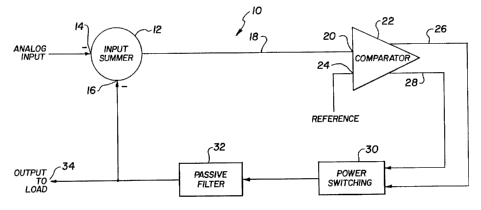
Fig. l, a block diagram of a power controller of the present
invention;
Fig. 2 is a block diagram of a modification of the present
invention illustrating the presence of an active filter and a
passive filter;
Fig. 3 is a circuit schematic of the input summer of Fig.
1.
Fig. 4 is a circuit schematic of an asynchronous comparator;
Fig. 5 is a circuit schematic of a suitable power switching
network;
Fig. 6 is a circuit schematic of a passive filter useful in
the practice of the present invention;
Fig. 7 is a circuit schematic of a synchronous comparator;
Fig. 8 is a circuit schematic of the input summer of Fig.
2, including an active filter of at least the third order;
Fig. 9 is a graph illustrating the gain frequency
characteristics of the passive filter response and active third
order filter response; and
Fig. l0 is a block diagram of a power controller of the
present invention, including pulse width modulation.
DETAILED DESCRIPTION
Referring now to Fig. l, there is illustrated one embodiment
of the present invention, a power controller l0. An input summer
12 has a first input 14 to which is applied an analog input
S~B~T~ SHEET (I~U' E 2~)
~ 094/17~88 215 4 ~ 9 0 PCT~S94/00512
signal and a second input 16 is applied a signal which is an
amplified inverted reproduction of the analog input derived from
the output of controller 10. The two signals are summed together
to create an error signal that represents the difference between
the two signals. Should the output signal be in phase with the
input signal, then the output signal would be subtracted from the
input signal to create the error signal. The error signal is
applied by way of conductor 18 to one input 20 of a comparator
22 where the error signal is compared with a reference signal
applied to input 24 of the comparator 2 Should the error
signal be greater than the reference signal, the minus control
of the comparator on conductor 26 goes low and the plus control
of the comparator 22 on conductor 28 goes high. Should the error
signal be of lower value than the reference or threshold voltage,
then the minus control of the comparator will go high and the
plus control of the comparator will go low. The minus control
and plus control outputs of the comparator 22 are applied to, and
control the operation of a power switching network 30. In the
event that the error signal is greater than the reference or
threshold voltage applied to input 24 of the comparator 22, the
plus control will go high and turn on the power switching device
30 to cause the output of the power switching network to become
more positive. In the event that the error signal is less than
the reference or threshold voltage, the minus control will
increase and turn on the power switching network 30 to cause the
output of the network to become more negative.
The output of the power switching network 30 is applied to
a low-pass passive filter 32, the filtered output of which is
applied as an output to a load, either resistive or reactive, and
also applied to input 16 of summer 12. Where the analog input
is greater than the output fed back to input 16 of the summer 12,
the error signal goes more positive, to correct the original
error.
The process continues at a high rate where adjustments are
3S made by power switching network 30, and produces an output that
tracks the analog input to reduce the difference called the error
signal. This difference is kept to a minimum by the operation
of the power switching network. By use of the switching means,
the analog input signal is faithfully reproduced as an amplified
signal applied to the load 34.
SUB~ L ~ Sr~ nt~L~
21~4490
WO94/17588 - PCT~S94/00512 -
Details of the input summer l2 of Fig. l are illustrated by
the clrcuit in Fig. 3 to inc~lude~an operational amplifier 40,
which sums the analog input~w:i'th the feed back from the output
at the amplifierls inverting input 42 with a DC offset signa~
applied to the non-inverting input 44. The output of the
amplifier 40 is buffered by a transistor 46, to provide the error
signal to be applied to the comparator 22 (Fig. l). Capacitor
48 is present to remove any unwanted DC component of the analog
input. If the D.C. component is desired, the capacitor 48 would
be eliminated. The ratio of resistors 50 and 52 set the gain for
the analog input signal. The feedback signal from the output is
attenuated by the resistors 54 and 56 in the frequency band of
interest. At very low frequencies, for example below 5 Hertz,
capacitor 58 causes an increased gain in the feedback signal to
facilitate the maintenance of a minimal DC offset. Capacitor 60
causes a boost in the high frequency components of the feedback
signal, outside of the frequency band of interest, and thereby
maintains stability of the closed loop system. The networl~
comprised of resistor 54, resistor 56, and capacitors 58 and 60,
together with the amplifier feedback resistor 52, set the gain
for the output feedback signal applied to the inverted input 42
of operational amplifier 40.
Resistor network comprised of resistors 62 and 64, together
with Zener diode 66, bias the operational amplifier 40, such
that the error voltage or signal applied to the comparator is
possessed of negligible error with respect to the comparator
reference voltage when the output signal is at a near zero DC
offset voltage. Capacitor 68 functions to filter out power
supply noise. It will be noted that the operational amplifier
40 inverts the sum of the analog input signal and the feedback
signal from the output, but does not invert the DC bias signal
applied to the non-inverting input 44. In as much as the
feedback signal from the output is inverted with respect to the
analog input signal, the error signal will be a small difference
of one signal canceling the other, plus a DC bias. Diode 70 is
present to clip the error signal from the operational amplifier
40 should the signal go too high or too low, and thus protect the
voltage comparator from abnormal voltage swings at its input.
Resistor 72 isolates the operational amplifier 40 from excessive
load when clipping occurs through diode 70. The error slgna]
applied to the base of transistor 46 is converted from a high
impedance signal to a low impedance signal by the transistor 4~)
SU~STi~ 3H~T ~ILt ~,
094/17588 21~ O PCT~S94/00512
and resistor 74. This low impedance error signal is then applied
to the voltage comparator.
Either a synchronous or an asynchronous comparator may be
utilized in the practice of the present invention. An
asynchronous comparator is illustrated in Fig. 4, comprised of
two (~) inverting gates 80 and 82. The output of gate 80 is the
minus control and the output of gate 82 is the plus control.
This asynchronous voltage comparator will change states every
time the error voltage changes polarity with respect to the
voltage comparator reference voltage. Suitable inverting gates
are available as part number 74HC04, from Texas Instruments.
A suitable synchronous voltage comparator is illustrated in
Fig. 7 to include a D flip-flop 84. The error signal is applied
to the D input. The reference or threshold voltage is about one-
half of the power supply voltage applied to the gates and this
reference voltage is the gate switching threshold voltage. A
gate's switching threshold voltage does not utilize a physical
voltage reference, but it is inherent in the design of the gate,
for example, a high-speed CMOS gate. A high frequency clock
signal, typically 50 to 500 times the frequency of the highest
frequency of interest in the analog input is applied to the clock
input CK of the D flip-flop 84. The highest frequency of
interest for high-fidelity audio is typically 20,000 Hertz. The
pre-set and re-set inputs, respectively P and R are connected to
the power supply, in this case a positive 5 volts, to disable
their operation. When the error signal is greater than the
reference or threshold voltage, the Q output becomes positive
or high, immediately following the positive going transition of
the clock pulse, and the inverted Q of output becomes zero or
low. When the error signal is less than the reference or
threshold voltage, the Q output becomes zero or low immediately
following the positive going transition of the clock pulse and
the inverted Q output becomes positive or high. A suitable D
flip-flop is available from Texas Instruments as part number
74HC74.
The two comparator outputs, plus control and minus control,
derived from either of the comparators illustrated in Fig. 4 or
Fig. 7 control the operation of the power switching network 30,
the details of which are illustrated in Fig. 5. The plus control
is applied to one input, pin 4 of a digital driver 90, which is
T~ S~E'~ U~ 26)
WO~ S~ PCT~S94/00512 -
a logic device available from National Semiconductor as part
number DS0026. The digital drivèr 90 applies an inverted logic
signal from its output, pin i; to a gate 92 of a Mosfet
transistor 94. In the pre~se~nt embodiment the other half of the
digital driver 90, represented by pins 2 and 7 is not used. sut,
pin 2 is grounded. The source pin S of the Mosfet transistor 94
is connected, for example, to a plus fifteen volt supply. The
value of the supply voltage determines the power rating of the
amplifier or power controller. The drain pin D of the Mosfet
transistor 9~ is connected to the filter input.
The minus control is connected to a current limiting
resistor 96 to the base of transistor 98. By connecting the
emitter of the transistor 98 to a plus five volt supply and the
collector of the transistor 98 to a minus fifteen volt supply,
through resistor 100, the logic signal minus control is converted
to an inverted signal operating between plus five volts and minus
fifteen volts. This inverted logic signal then drives the base
of transistor 102 through current limiting resistor 104. A
positive five volt voltage regulator 106 is connected between
ground and minus fifteen volts such that itls output will be five
(5) volts more positive than minus fifteen volts. Capacitor 107
is a filter. The collector of transistor 102 is connected to the
output of voltage regulator 106, and the transistor emitter is
connected to minus fifteen volts through resistor 108. When the
base of transistor 102 is driven by the inverted logic signal
derived from the minus control, the transistor's emitter will
vary from minus fifteen volts to minus ten volts. This varying
voltage from the transistor 102 is applied to input pin 4 of a
digital driver 110. The digital driver 110 has the same part
designation as the digital driver 90. A ground connection to pin
6 of the digital driver 110 is utilized as the positive supply
for the driver. Pin 3 of the digital driver 110 is connected to
minus fifteen volts as a negative supply. The inverted logic
signal occurring at pin 5 of the digital driver 110 is applied
to gate 112 of Mosfet transistor 114. As in the case with
digital driver 90, only one-half of the digital driver 110 is
utilized. Pins 2 and 7 are not used, although pin 2 is connected
to a minus fifteen (-15) volt supply. The source pin S of the
Mosfet transistor 114 is connected to a minus fifteen
volt supply, and the Mosfet transistor drain, pin D is connected
to the filter input.
SlJBS~TUTE SH~E, (~ut ~ 26)
WO94117588 215 ~ ~ 9 PCT~S94/00512
The plus control and minus control will not both be high or
positive at the same time, except for possibly for a very short
switching transition period. When the plus control goes high,
the input to digital driver 90 goes high, and its output goes
low, causing Mosfet transistor 94 to turn on, and provide a very
low impedance path, such that when the Mosfet transistor 94 is
on, the output to the filter input will be a plus fifteen volts.
Mosfet transistor 114 will be turned off at this time. When the
minus control goes high, transistor 98 will be turned off, and
its collector will go to minus fifteen volts. As a result,
transistor 102 will be biased off, and it's emitter will go to
minus fifteen volts. Output of digital driver 110 will now go
high, causing Mosfet transistor 114 to provide a very low
impedance path. As a result, a full minus fifteen volts will be
applied to the filter input. When the minus control is low, the
transistor 98 will be on, with it's collector voltage near plus
five volts. Transistor 102 will be on, causing it's emitter to
be near minus ten volts. This minus ten volts signal is seen as
a logic high by digital driver 110 and it's output at pin 5 will
be low, minus fifteen volts, causing Mosfet transistor 114 to
turn off. The Mosfet transistors 94 and 114 are selected for
high switching speeds and for providing very low impedance or
resistance paths, typically less than one ohm. When the plus
control is high, the output applied to the filter input will be
high or a plus fifteen volts. When the minus control is high,
the output applied to the filter input will be low, for example
minus fifteen volts. The circuit is designed to prevent both
output switching transistors, namely the Mosfet transistors 94
and 114, from being on at the same time.
In normal operation, pulses from the power switching network
30 will vary at a high frequency, between plus and minus fifteen
volts, with an average value that is proportional to the analog
input signal.
The output of switching network 30 is applied to a low-pass
filter, illustrated in ~ig. 6. The low-pass filter 32 is ~
passive filter, comprised of inductor 116 and capacitor 118. The
values of inductor 116 and capacitor 118 are chosen to provide
a filter cut-off above the highest frequency to be amplified, but
well below any switching frequency. Resistor 120 is a bleeder
resistor that drains the capacitor 118 under no-load conditions.
The load itself can be resistive, or perhaps somewhat reactive,
Sl!BST~TU~ S~EE5 (RULE 2~)
215~90
WO94tl7588 PCT~S94/00512 -
and of low impedance, such as 4 ohms. A common load would be a
speaker voice coil. The passive low-pass filter 32 will
attenuate any high frequency switching noise generated by the
power switching network 30, and will produce an output that is
a relatively noise-free analog signal proportional to the analog
input signal. The principal purpose of the filter 3 is to
satisfy FCC regulations regarding radiation of high-frequency
noise, which otherwise could result if the conductors to the load
are very long and unshielded.
The difference between the analog signal at the input and
the analog signal at the output is an error signal that can be
viewed as broad band coherent noise with the frequency of the
noise extending to one-half the clock frequency. Should it be
desired to reduce the coherent noise in the band of interest, for
example, up to 20,000 hertz, the error signal must be filtered
before it arrives at the voltage comparator, so that the voltage
comparator will make better decisions based upon the error signal
below ~0,000 hertz, and be less influenced by errors above 20,000
hertz and the signal-to-noise ratio will be significantly
increased below 20,000 hertz. One manner of accomplishing this
is to make the passive filter a higher order filter.
Alternatively, as shown in Fig. 2, the higher order filter may
be provided by the components within block 130. These components
include the input summer 112, together with filter 113.
Details of the block 130 are illustrated in the circuit
schematic of Fig. 8, which provides at least a third order low-
pass filter, preferably under-damped, to improve the output
signal's signal-to-noise ratio and linearity. The circuit of
Fig. 8 comprises five main stages provided by four operational
amplifiers 132, 134, 136, and 138, together with transistor 140.
Amplifier 132 is an inverting amplifier which includes an input
summer and a third order filter. Amplifier 134 is an inverting
amplifier. Amplifier 138 is a buffer amplifier preceded by a
high-pass filter. Amplifier 136 is an inverting amplifier that
also sums the third order filtered error signal at a high level,
with the output signal altered by a high-pass filter at a lower
level. Transistor 140 is a buffer that drives the input to the
voltage comparator. The operational amplifiers are available
from Precision Monolithics as part number OP-37, and the
transistor is available from RCA as part number SK3931.
~U~ T~ S~iE.T (RULE 26)
~ 094/17588 21~ ~ ~ 9 0 PCT~S94/00512
The design of higher order filters is described in the text
"Design of continuous ana digital electronic systems" by Gordon
J. A. Bird published by McGraw-Hill Book Company tUK) Limited in
1980. An underdamped active filter is one in which the filter
is damped sufficiently to prevent oscillation of the output
following an abrupt input stimulus.
There will now be undertaken, a detailed description of the
circuit illustrated in Fig. 8. Capacitor 147 is present to
remove anv unwanted DC component of the analog input. If the DC
component is desired, then the capacitor will be eliminated. The
ratio of the impedance of the feedback circuit 144, between the
output of operational amplifier 132 and its inverting input, and
resistor 146, determines the gain for the analog input signal.
The feedback signal from the output is attenuated by resistors
148 and 150 in the frequency band of interest. At very low
frequencies, such as those below five Hertz, capacitor 152 causes
increased gain in the feedback signal so that it is easier to
maintain a minimal DC offset. The network of resistor 148,
resistor 150 and capacitor 15~, in combination with the amplifier
feedback circuit 144, sets the gain of the amplifier stage for
the output feedback signal. The amplifier feedback signal 144
is comprised of resistors 154, 155, and 156, together with
capacitors 158, 160 and 162. The use of the above described
feedback circuit 144, with the operational amplifier 132,
achieves a third order low-pass filter. It is critically, or
less than critically damped, and preferably under-damped.
Amplifier stage 134 inverts the signal and has its gain set
by input resistor 164 and feedback resistor 166. The output of
the amplifier stage 134 is again inverted by operational
amplifier 136 whose gain is set by input resistor 168 and
feedback resistor 170.
In order to maintain stability in the closed loop system,
it is necessary to reduce the slope of the response of the third
order filter. The frequency response of the filter is
illustrated in Fig. 9 and where there is applied a high-pass
response to the output signal to create a filter zero at about
180,000 Hertz. This signal is added at a low level to the signal
from the third order filter. The resulting filter response is
shown by the solid line in the graph of Fig. 9. After the
peaking caused by the underdamped characteristic of the filter,
the filter slope decays at about 60dB per decade until the error
.. 11
S~3~ST~U~E SH~, (RULE 26)
21S4490
WO94/17588 PCT~S94/00512
signal is dominated by the response of the passive filter which
is a second order filter. At this higher frequency the slope
changes to a 40dB per decade slope typical of a second order
filter. At an even higher frequency, the slope changes to 20dB
5per decade slope typical of a first order filter. Had the third
order active filter described been a;fi~th order filter, then the
initial filter slope would have~been lOOdB per decade. The
higher order filter more greatly`reduces the error signal outside
of the band of interest and enhances the correctness of the
10comparator decisions made on the error signal in the band of
interest. Hence, the analog output will have reduced error
within the band of interest when compared to the input analog
signal and will thus have improved signal-to-noise ratio and an
improved linearity. The summation of a low-level representation
15of the analog output with the initial higher order error signal
causes a reduced attenuation slope to high frequency error
signals, but allows for a reduction in phase shift so that
stability can be maintained. A zero or high-pass function is in
series with this representation of the analog output to further
20reduce the phase shift to further insure stability at higher
frequencies. The zero or high-pass function is achieved with
resistors 172 and 174, together with capacitor 176. The output
signal from the power switching network (Fig. 1) has been
processed by a second order low-pass filter 32 and the high-pass
25filter represented by resistors 172, 174, and capacitor 176 is
buffered by operational amplifier 138, whose gain is set by
resistors 178 and 180. The output of the operational amplifier
138 is then summed with the third order filter output, at the
inverting input of operational amplifier 136. The gain to the
30signal applied from operational amplifier 138 is set by the
inverting amplifier 136, input resistor 182, and feedback
resistor 170. The operational amplifier 136 also provides a bias
voltage such that the DC error voltage at the comparator has
almost no error with respect to the comparator reference voltage
35when the output signal has a near DC offset voltage. The bias
voltage is set by resistors 184 and 186, together with Zener
diode 188. The capacitor 190 filters out the power supply noise.
The voltage comparator is protected from abnormal voltage
swings at its input by the diode 192 which clips the error signa~
40if it goes too high or too low. Resistor 194 isolates the
operational amplifier 136 from the excessive load that would
occur if clipping occurs through the diode 192. The error slgnal
S~ I ITl~T~ S'~ET (R~I~E 26)
094/17588 ~ 9~ PCT~S94/00512
present at the base of transistor 196 is converted from a high
impedance signal to a low impedance signal by the transistor 140,
together with resistor 198. The error signal is then applied to
a voltag~ comparatol-, eithel- to th~ or-e shown in Fiy. 4 or th~
synchronous comparator shown in Fig. 7.
A number of modifications are possible. The passlve low-
pass filter in Fig. 6 could be eliminated entirel~-. It is
possible to drive some loads directly with the output of the
power switching network 30, where the load acts as the integrat:o~-
of the switching pulses to provide a more continuous lower
frequency drive to the load. However, there needs to be a
filter between the output of the power switching network and the
voltage comparator to improve the ability of the comparator to
make decisions on the errors in the frequency band of interest.
It is unnecessary to operate on the signal coming from the analog
input with a filter. The analog input can be added into the
circuit at any point, right up to the voltage comparator. Only
the signal fed from the power switching network must be filtered
before it arrives at the voltage comparator. As a matter of
convenience, the analog input and the inverted reconstruction of
the analog input, the output signal, are added together to create
a much smaller signal representing the error, which is the
difference between the two signals. By creating the error or
difference signal early in the process the amplifiers can have
a much lower dynamic range and increased linearity in as much as
they do not need to amplify the entire signal, but just the error
or coherent noise.
~IG. 10 is a schematic block diagram showing the invention
applied with a pulse width modulator ~PWM). An audio signal is
applied to one input of input summer 200 which produces a signal
which is the difference between the audio signal and a
representation of that signal fed back from the output of filter
21~ by way of conductor 202. The difference signal is applied
to an active filter 204 of at least the third order which
produces an output of high signal-to-noise ratio and linearity.
The filtered signal is supplied to PWM 206. A triangle-wave
carrier signal with a frequency of, for example, 430 KHz is
supplied from a triangle-wave generator 208 to the PWM 206. The
PWM 206 may be comprised of a level comparator and adapted to
compare the level of the error or difference signal with that of
the reference triangle-wave signal to generate a rectangular-wave
~ST~TUTE SH~T (RiJ~E 26~
WO94/17588 PCT~S94/00~12
pulse width modulated signal whose pulse width varies according
to the instantaneous amplitude level and polarit~ of the
modulating difference signal. The PWM si.gnal is amplified by
output amplifier 210. The output amplifler 210 is a swltching
amplifier like the power switching network 30 of FIG. 5 whose
output of discrete positive and negative pulses is applied to a
passive low-pass filter 212. The low-pass filter supplies to a
load, such as a loud speaker, an amplified, true representation
of the input audio signal.
While the invention has been illustrated and described in
detail in the drawing and foregoing description, the same is
considered as illustrative and not restrictive in character, it
being understood that only the preferred embodiments have been
shown and described and that all changes and modifications that
come within the spirit of the invention are desired to be
protected.
14
S~ST~ E S~ (RlJ~ 26)