Note: Descriptions are shown in the official language in which they were submitted.
~154699
WO95/l4963 - ~ PCT~S94/03564
l!
ENERGY SAVING POWER CONTROL SYSTEM
Technical Field
This invention relates generally to the field of
electronic power regulation and control; and, more
specifically, to a power regulation apparatus and
method for reducing energy consumption of a load,
particularly inductive loads such as fluorescent
lights and motors, while simultaneously shifting the
power factor toward a leading reflected power factor,
and maintaining low line harmonic distortion, low line
crest factor, and low line noise.
Backqround Art
A variety of AC power regulating circuits are
known in the art in which AC power to a load (e.g.,
fluorescent lamps, motors, etc.) is regulated through
control of an AC electronic switch (e.g., a thyristor)
interconnecting the source of the AC power and the
load. Many of these systems use some form of feedback
control system to sense the load power. This
information is then used to advance or retard the time
relative to the initial zero crossing that the
electronic switch is triggered into conduction during
each half cycle of the AC power cycle. Thus, the
device is turned on later in the cycle to reduce power
and earlier to increase power. Once activated, the
electronic switch typically turns off automatically
thereby blocking current to the load when the load
current reverses direction (i.e., at the zero
crossing) as illustrated in Fig. lA. For example,
some prior art systems utilize a triac as an
electronic switch because of its bi-directional
conduction and high power characteristics. However, a
triac only turns off when the current through the
triac drops to zero. Thus, to decrease or increase
WO95/14963 PCT~S94/03564
` 2~ 2-
the power to the load, the trigger phase angle is
advanced or retarded and the portion of each half wave
of AC input power which is applied to the load through
the switch is thereby decreased or increased.
Power regulation of this type results in
conduction occurring primarily during the later part
of each half cycle of the AC power. This tends to
cause an inductive (lagging) power factor, generates
harmonic distortion and noise spikes reflected into
the power line and causes a high crest factor. Such
lagging power factors decrease power line efficiency
(i.e., increase power line current for a given load
power consumption) and frequently results in increased
electric utility rates to the user. In addition,
because current does not flow from the AC source
during the time the electric switch is turned off,
substantial harmonic distortion and noise is reflected
into the power line which can interfere with the
operation of sensitive electronic equipment.
In another type of prior art power regulation
circuit, an electronic switch is turned on and off
several times during each half cycle to control the
current to the load, as illustrated in Fig. lB.
Inductive energy is dissipated by switching a short
circuit across the load when the electronic switch is
turned off. This type of circuit also can produce or
aggravate an inductive power factor, and generates
harmonic distortion, noise, and a high crest factor on
the AC power line. Thus, EMI and RFI filtering is
re~uired.
In either type of prior art regulating circuit,
current from the AC power line to the load is
interrupted during a substantial portion of each AC
half cycle which can result in large surge currents.
This large surge current can cause ballast temperature
to rise excessively causing early failure or actual
breakdown with acrid smoke generation. In addition,
Wo95/14963 21 5 ~ 6 9 9 PCT~S941~3564
when used to power lighting loads, such as fluorescent
lights, at a reduced power level to conserve power,
these circuits cause a large reduction in light
output.
It is, accordingly, an object of the present
invention to provide a novel, economic and reliable
method and apparatus for AC power regulation which
permits reduced power consumption while providing a
leading power factor and m in;~;zing the reflected
harmonic distortion, noise spikes and crest factor on
the AC power line.
It is another object of the invention to provide
a novel method and apparatus for AC power regulation
which is self-adjusting for a wide range of loads.
It is another object of the invention to provide
a novel method and apparatus for AC power regulation
which provides a 25 percent reduced power consumption
for fluorescent and other ballasted lighting loads
without excessive light intensity loss while providing
a leading power factor.
It is another object of the invention to provide
a novel method and apparatus for AC power regulation
utilizing a triac and a large parallel energy transfer
capacitor substantially greater than l~f in which
current continues to flow through the load via the
capacitor during the time the triac is off so that
current flows during substantially all of the AC cycle
and a substantial portion of the power to the load is
provided by current flowing through the capacitor. It
is another object of the invention to provide a novel
method and apparatus for AC power regulation utilizing
a triac and a parallel switched energy transfer
capacitor bank, wherein the triac is switched on
shortly after the zero crossing of each half wave of
the AC cycle and is switched off when an adequate
power level is reached substantially before the next
zero crossing to provide a leading power factor.
WO95/14963 ~i 5 4 ~ 9 9 PCT~S94/0356
--4--
Disclosure of the Invention
Briefly, according to one embodiment of the
invention, there is provided an AC power regulation
system for controlling power to a load having an input
for coupling to an AC power source for supplying AC
power having zero current crossing points at the end
of each half cycle and wherein the system includes an
output for coupling to the load. The system includes
a triggerable switch coupled between the input and the
output, a capacitor bank for supplying an energy
transfer capacitance coupled in parallel with the
triggerable switch, a circuit for generating power
sense signals responsive to the load power, means for
triggering the triggerable switch into a state of
conduction, and means for switching the triggerable
switch into a non-conductive state. Control circuitry
is provided, coupled to the means for triggering and
the means for switching, for generating control
signals responsive to the power sense signals to
control the means for triggering and the means for
switching such that the electronic triggerable switch
is triggered to a conduction state at a selected turn-
on time after each zero crossing, and switched back to
the non-conducting state at a selected turn-off time
before the next zero crossing. The selected turn-off
time is chosen to obtain a desired power level and to
improve the reflected power factor responsive to power
sense signals. In another embodiment, the capacitor
bank comprises a bank of switchable capacitors and the
control circuitry comprises circuitry for generating
control signals to switch the switchable capacitors to
obtain a selected capacitance responsive to the power
sense signals.
In one embodiment of the invention, a monitor
circuit is coupled across the triggerable switch to
generate a differential voltage signal responsive to
the voltage across the triggerable switch. A
WO95/14963 PCT~S94/03564
2 ~
--5--
controller circuit operates to triggér the triggerable
switch into a conductive state responsive to the
differential voltage signal. In addition, the means
for switching the triggerable switch into a non-
conducting state may switch the triggerable switch by
shunting current around the triggerable switch for a
short period of time.
Brief DescriPtion of the Drawings
The features of the present invention which are
believed to be novel are set forth below with
particularity in the appended claims. The invention,
together with further objects and advantages thereof,
may be understood by reference to the following
description taken in conjunction with the accompanying
drawings.
FIGS. lA and lB are waveforms of current through
the load control device for prior art power regulation
devices.
FIG. 2 is a generalized block diagram of one
embodiment of a power regulation circuit in accordance
with the present invention.
FIG. 3 is a waveform of the current through the
load control switch for a power regulation circuit in
accordance with the present invention.
FIG. 4 is a detailed block diagram of one
embodiment of a power regulation circuit of FIG. 2 in
accordance with the invention.
FIG. 5 is a detailed circuit diagram illustrating
one embodiment of the microprocessor circuit of FIG. 4
according to the present invention.
FIG. 6 is detailed circuit diagram illustrating
one embodiment of the electronic switch, capacitor
bank and opto-coupler circuits of FIG. 4 according to
the present invention.
FIG. 7 is a detailed circuit diagram illustrating
one embodiment of the pulse switch and power supply
circuits of FIG. 4 according to the present invention.
WO95/l4963 2 ~ $ ~ ~ PCT~S94/03564
FIG. 8 is a detailed circuit diagram illustrating
one embodiment of the power-on reset circuit of FIG. 4
according to the present invention.
FIG. 9 is a detailed circuit diagram illustrating
one embodiment of the over-voltage circuit of FIG. 4
according to the present invention.
FIG. 10 is a detailed circuit diagram
illustrating one embodiment of the reset circuits of
FIG. 4 according to the present invention.
FIG. 11 is a detailed circuit diagram
illustrating one embodiment of the driver circuits of
FIG. 4 according to the present invention.
FIG. 12 is a detailed circuit diagram
illustrating one embodiment of the power sense circuit
of FIG. 4 according to the present invention.
FIG. 13 is a detailed circuit diagram
illustrating one embodiment of the voltage regulator
circuit of FIG. 4 according to the present invention.
FIGS. 14 to 15 are exemplary waveforms for
various signals occurring in the power regulation
circuit of FIG. 4.
FIG. 16 through 20 are detailed flow charts
illustrating the functional operation of the system
and the programmed microprocessor for one embodiment
of FIG. 5.
Best Mode for CarrYinq Out the Invention
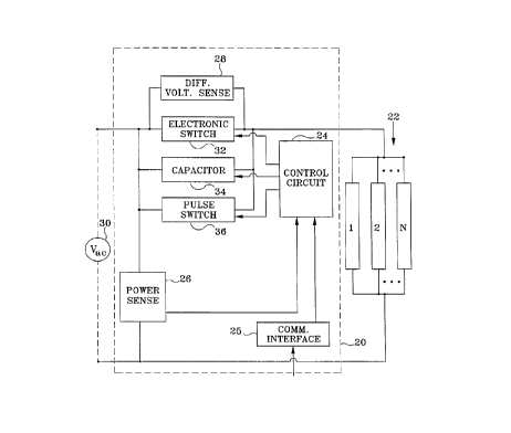
Referring to Fig. 2, there is shown a generalized
block diagram of one embodiment of a power regulation
system 20 for conserving AC electrical power
consumption by a load 22, typically made up of a
plurality of individual devices according to the
invention. The system 20 is particularly suited for
supplying power to multiple light fixtures such as
fluorescent, metal halide, mercury vapor, high
pressure or low pressure sodium light fixtures, etc.
The system 20 is controlled by a control circuit 24,
which in the illustrated embodiment of Fig. 4 is a
woss/l4963 2 1 5 4 6 9 9 PCT~594/~3564
programmed microprocessor, but which may be any
combination of analog and/or digital control circuitry
capable of generating the required control signals.
The control circuitry 24 may also include a
communication interface 25 to permit external
communications with the control circuit 24 (e.g., a
serial RS-232 communications interface). Where
external communications are involved, the system 20
may include suitable electrical isolation for the
communication lines, such as use of opto-couplers or
other isolation techniques well known in the art. The
control circuitry 24 is responsive to sense signals
coupled from a power sensing circuit 26 in series with
the AC power source 30, and to a differential voltage
signal coupled from a differential voltage sense
circuit 28, as shown. The power sensing circuit 26,
in the illustrated embodiments of Figs. 4-13, senses
the line voltage and current, and derives power value
by multiplying voltage and current in a multiplier
circuit.
The differential voltage sense circuit 28 is
coupled across an electronic triggerable switch 32
which is also in series with the AC power source 30
and the load 22. The differential voltage sense
circuit 28 generates a signal indicative of
approximately zero voltage across the electronic
switch 32 which is used to determine the turn-on time
of the electronic switch 32. The electronic switch 32
controls power to the load 22 under control of the
control circuit 24. An energy transfer capacitor
circuit 34 capable of supplying a large capacitance
(e.g., substantially greater than l~f) and a pulse
switch circuit 36 are coupled in parallel with the
electronic switch 32, as shown. The electronic switch
32, capacitor circuit 34, and pulse switch circuit 36
are controlled by control signals coupled from the
control circuit 24.
WO95/14963 PCT~S9~/0356~ ~
21~ ~99 -8-
In the system 20 of Fig. 2 in accordance with the
invention, the electronic switch 32 is switched on in
a unique manner. The electronic switch 32 is turned
on by a signal from the control circuit 24 shortly
after the zero crossing of the AC line voltage in
response to detection by the differential voltage
circuit 28 of a zero or near-zero voltage across the
electronic switch 32. Consequently, electronic switch
32 is typically turned on during the first 15 to 40
degrees of each half cycle of the AC line voltage sine
wave. The switch 32 is turned off thereby blocking
current through it when the desired power level is
reached, typically near the peak of each half cycle of
the AC line voltage sine wave (i.e., near 9o and 270
degrees) instead of at the next zero crossing at the
end of each AC half cycle. A typical example of
resulting current through the switch 32 is illustrated
by the waveform of Fig. 3 which differs dramatically
from that of the prior art devices illustrated in
Figs. lA and lB. This switching is accomplished by
activating the pulse switch 36 to shunt the load
current around the electronic switch 32 for a brief
period (e.g., 180 microseconds) to permit the
electronic switch 32 to turn off. In this manner, the
current conducted by the switch 32 thus can be largely
confined to the first and third quadrant of the AC
line voltage sine wave when it is desired to reduce
power to the load. The pulse switch 36 is activated
by a signal from the control circuit 24.
The capacitor circuit 34 prevents an excessive
dv/dt from falsely firing the electronic switch 32,
and stores inductive energy from the load when the
electronic switch 32 is turned off. During a savings
mode when power is reduced, the capacitor circuit 34
also permits substantial AC current to flow through
the load when the electronic switch 32 has been turned
off, the load 22 is still connected to the power line
WOgS/14963 PCT~S9~/03564
~154699
in series with the capacitor circuit 34 so that a
substantial portion of the power to the load
(typically, 40-50 percent of the total power in the
illustrated embodiment for a ballasted lighting
fixture load) is supplied through the capacitor
circuit 34. The capacitor circuit 34 also permits
selection of capacitance prior to entering the savings
mode to match capacitance to the load under control of
the control circuit 24 by means of a bank of switched
capacitors.
This unique manner of triggering the turn-on of
the switch 32 in response to a near-zero voltage
together with the turn-off of the switch 32 at or near
the peak of the AC line voltage half cycle shifts the
power factor toward a leading power factor as seen by
the AC power source. The energy transfer capacitor
circuit 34 absorbs reactive voltage spikes caused by
the collapsing magnetic field of inductive loads when
the electronic switch 32 is turned off and provides
additional power factor lead, reduction of harmonic
distortion, reduced crest factor, and reduced noise
spikes reflected into the power line. Thus, the
system 20 either reflects a leading power factor or,
at a minimum, shifts a lagging power factor so as to
reduce the amount of lag thereby shifting toward a
leading power factor (i.e., closer to a pure resistive
power factor). In addition, the capacitor circuit 24
permits current to flow to the load when the switch 32
is turned off thereby extending lamp arc conduction
time in each half-cycle of operation of lamps such as
fluorescent lamps increasing the efficiency of the
fixture and minimizing the light loss during reduced
power operation. Optionally, additional switching
circuitry in the capacitor circuit 34 permits
selection of a range of capacitor values to permit
dynamically matching the capacitance to the load type
and current under the control of the control circuit
WO95/14963 PCT~S9~/03564
2 1 r 10
24. The leading power factor generated by the system
20 can be combined with undesirable lagging power
factor conditions caused by other loads such as motor-
driven appliances and equipment (e.g., air
conditioners) to provide a more desirable overall
power factor.
The system 20 of Fig. 2 can be configured to use
the inventive switching scheme together with the
inventive capacitor circuit 34 to provide large energy
savings (25 percent in the savings mode in the
illustrated embodiment of Fig. 4) while still
providing a leading power factor by providing a
selected reduction of power to the load under control
of the control circuit 24. In this energy-saving
mode, power reduction is accomplished primarily by
controlling the point at which the electronic switch
32 is turned off, thereby controlling the portion of
the AC cycle (i.e., the conduction angle) during which
current is permitted to flow through the electronic
switch 32.
In one embodiment, the system 20 can operate in
four operational modes. An initial power turn-on mode
begins when the main power is switched on and ends
when the control circuit 24 is fully initialized.
During this mode, the electronic switch 32 is held off
and only minimal current through the capa~citor 34 is
supplied to the load. When the control circuit 24 is
fully operational, it generates a control signal to
turn on the switch 24 each time the zero or near-zero
voltage across the switch 32 is detected by
differential voltage sensor 28. As a result, the load
is supplied with full power.
The power-on mode is followed by a warm-up mode
for a selected period of time (e.g., selected based
upon load type and warm-up requirements) during which
the control circuit 24 samples and digitizes a power
measurement, an rms current measurement and an rms
W O 95/14963 21~ ~ 6 9 ~ PCT~US94/03564
--11--
voltage measurement for successive sample periods from
the power sense circuit 26. These values are compared
to the same measurement from the two prior samples
until a stable average value is obtained. Final
measured values are stored when the current
measurement is sufficiently stable for a predetermined
period of time (e.g., 32 seconds). This final value
is used to select the desired amount of capacitance
for the capacitor circuit 34. The final average power
is stored and 75 percent of that value is calculated
and stored as the target reduced power level that the
system 20 will maintain during the savings mode.
After the warm-up period, a transition-to-savings
mode is entered. The transition period is begun by
switching the capacitor circuit 34 to bring its
capacitance to the selected value and the conduction
time of the switch 32 is then gradually shortened
until the 75 percent calculated power level is
reached. Once the system 20 is at equilibrium, the
savings mode is entered in which the power savings is
maintained and the system 20 tracks changes in load
power, line voltage, and load current. Changes in
power due to line voltage change or due to small
current changes result in adjustment of the conduction
time of the switch 24 to maintain the calculated
power. If a large change in current (e.g., over 20
percent) occurs, the system circuit 22 will recycle to
the warm-up mode where a new target reduced power and
new capacitance level will be selected. The threshold
for a large change in current is set to detect
significant changes in load (i.e., addition or
deletion of a fixture) while ignoring normal current
variations and spikes. Thus, a typical value in the
illustrated embodiment would be approximately 20
percent of full load.
Referring now to Fig. 4, there is shown a
detailed block diagram of one embodiment of the power
WO95/14963 ~5 ~ PCT~S9~/03564
-12-
regulation system 20 according to the invention. The
system 20 includes a control circuit 24 comprising a
microcomputer 50 coupled to switch and jumper circuits
56 and driver circuits 52 to which is coupled a power-
on reset circuit 54, as shown. The microcomputer 50
couples output control signals to the pulse switch
circuit 36, to the capacitor circuit 34 composed of a
switched capacitor bank 58 and a capacitor 60, and to
the electronic switch 32. Signals are coupled from an
opto-coupler 62 which functions as a differential
voltage sensor 28, and from opto-couplers 64 through
the drivers 52 to the microcomputer 50. Signals are
also coupled directly to the microcomputer 50 from the
opto-couplers 64, the power sense circuit 26, and an
over-voltage trip circuit (OVT) 68, as shown. In
addition, a power supply 70 and voltage regulators
circuit 72 provide +150 volt, +12 volt, -5 volt, and
-12 volt power to the various circuits of the system
20. Also shown in Fig. 4 is a series resistor 76 in
series with the AC line which is used by the sense
circuit 26 for sensing line current.
Fig. S is a detailed circuit diagram illustrating
one embodiment of the microcomputer 50 including a
programmed microprocessor 100, lK-bit EEPROM 102, and
a 2.1 megahertz clock crystal 104. The microprocessor
100 (e.g., a MC68HC05 marketed by Motorola), which
includes internal A/D converters (not shown),
digitizes and accumulates voltage (E), current (I),
and power (W) data, and receives other input signals,
as shown. In addition, the microprocessor 100
performs calculations, stores the results of the
calculations, and generates various control signals
responsive to the input signals and calculations. The
program for the microprocessor 100 is stored in
internal memory. Forty-eight-hour burn-in data and
2160 hours of accumulated data can be stored in the
EEPROM 102.
WO95/14963 i ~ PCT~S94/03564
~ 63~
The input to the microprocessor 100 illustrated
in Fig. 5 includes 13 input signals and a three-bit
memory bus (SDA, SCL, WP) coupled to the EEPROM 102.
In addition, there are ten output control signals from
the microprocessor 100. The input signals include
three signals to the A/D converter input ports which
include E (voltage), I (current), W (power). The I
signal is a variable current DC signal representative
of the RMS AC current generated by the power sense
circuit 26. The signal voltage I is derived from the
current flowing through the resistor 76 in series with
the AC line. The E signal is a variable voltage DC
signal representative of the RMS line voltage
generated by the power sense circuit 26. The voltage
signal E is derived from the DC line voltage between
line and neutral. The input W is a variable power DC
signal generated by multiplying the AC voltage and
current signals in a multiplier circuit prior to
conversion to RMS DC values.
The rest of the input signals to the
microprocessor 100 are input on ten I/O ports. The
signal VCS is an adjustable voltage proportional to
the load current which is used for the determination
of the capacitor combination selection. ZX is a near-
zero crossing logical low pulse generated by inverting
a high pulse generated by the opto-coupler 64 each
time the voltage sine wave crosses the zero voltage
point. The ZD signal is a near-zero differential
logical low pulse generated by inverting a high pulse
generated by the opto-coupler 62 each time the voltage
across the electronic switch 32 is below a
predetermined threshold near zero. The signal OVT is
the over-voltage trigger signal generated by the OVT
circuit 68 which is normally a logic low and goes high
whenever the peak positive voltage across the switch
32 exceeds 500 volts. The generation of this signal
will cause the selection of the next larger
WO95/14963 ~ 9 9 PCT~S94/0356
-14-
capacitance and after three attempts will cause the
microprocessor 100 to turn off the main electronic
switch 32 and flash a fault condition LED. The IRST
input signal is an internal reset signal which is
generated by an internal switch of the switch and
jumper circuit 56 which is used to shorten the warm-up
period for production testing. The PORST signal is
the power-on reset signal generated by the power-on
reset circuit 54 which generates a logical high
voltage signal a short delay period after power is
turned on. The SHR signal is a 48-hour timer signal
which is generated by activating the appropriate
switch of switch and jumper circuit 56 as shown. The
WSA and WSB signals are two signals from the jumper
portion of circuit 56 which are used to select one of
four warm-up time periods. A 48-hour enable signal is
internally generated by the microprocessor 100 to
enable the 48-hour reset function after the designated
48-hour period has elapsed. A 2160-hour enable signal
is similarly generated. The SD signal is the sine
direction signal generated by the opto-coupler 64 from
which the processor selects the correct turn-off pulse
phase.
There are ten digital control signals generated
by the microprocessor 100 which control the various
functions of the system 20. The CAl, CA2, CA4 and CA8
are signals coupled to the capacitor bank 58 which
activate the appropriate capacitor combination to
obtain the desired capacitance determined by the
microprocessor 100. The TRlAC signal is a control
signal which controls the main electronic switch 32
and is a low signal to turn the switch 32 on and a
high when the switch 32 is to be off. The T01 signal
is a control signal which activates the pulse driver
to generate a turn-off pulse during the positive half
cycle and is a momentary low signal to turn off the
electronic switch 32. The T02 signal is the second
WO95/14963 PCT~S94/03564
~15~9
-15-
turn-off signal which controls turn-off of the pulse
driver during the negative half cycle and is a
momentary low signal to turn-off pulse the electronic
switch 32. The signal SI is the savings mode
indicating signal which is coupled to an indicator LED
to indicate when the system 20 is in the savings mode.
The FCI signal is a fault condition indicating signal
which turns on and flashes a fault-indicating LED when
a fault condition occurs. Among the fault conditions
detectable by the microprocessor 100 in the
illustrated embodiment are: 1) repeated OVT signals;
2) ZD stays high; and 3) ZD stays low. The FPI signal
is a full power indicator signal which turns an amber
LED indicator when not in savings mode or on and off
at a one-second rate when a 48-hour warm-up period is
in progress, and at once every three-second rate when
within the 2160-hour operating period. All three LED
indicators flash when an overload condition occurs.
Fig. 6 is a detailed circuit diagram illustrating
one embodiment of the electronic switch 32, the
capacitor circuit 34, and the opto-coupler 62. In the
illustrated embodiment, the electronic switch 32
comprises a main Triac 110 (e.g., a Q6040 manufactured
by Teccor) and a parallel varistor 112 connected in
series with the sense resistor 76 between a lir.e
terminal 114 and a load terminal 116, as shown. The
main Triac 110 is triggered by a TRIAC signal from the
microprocessor 100 coupled to the gate of the main
Triac 110 through a driver circuit 118 which amplifies
the processor output signal to the current level
required to drive the gate. Preferably, the specific
triac chosen will have a low gate drive current
requirement to minimize overall circuit power
consumption during triac conduction for efficient
operation. The varistor 112 protects the Triac 110 by
limiting high voltage transients across the main Triac
wos5ll4963 PCT~S91/0356~ -
~154~9 t
-16-
110, and the inductor 113 limits peak current to
protect the Triac llO from di/dt breakdown.
Of course, it will be understood by persons of
ordinary skill in the art that alternate forms of
switching, such as power FETs, power transistors and
the like, can be used in place of a triac. In an
alternative embodiment, for instance, power FETs could
replace the main Triac llO and the pulse transformer
158, thereby coupling directly to the load. The
relatively high voltage drop across the FETs, however,
would generate greater power losses than the preferred
circuit described herein.
The capacitor circuit 34 is coupled in parallel
with the Triac 110 and comprises a bank 58 of four
switchable capacitors C1 to c4, a capacitor C5, four
inductors 120, four Triacs 122, 124, 126, 128 and four
drivers 130 configured in a series - parallel network,
as shown. The Triacs 122, 124, 126, 128 (e.g., four
Q6015 triacs manufactured by Teccor) are switched
respectively by selection signals CA1, CA2, CA4, and
CA8 coupled from the microprocessor 100 through the
drivers 130. The drivers 130 amplify the
microprocessor 100 signals to the required current
level to drive the gates of the Triacs 122, 124, 126,
128. The inductors 120 limit peak switching currents
to protect the Triacs 122, 124, 126, 128 from di/dt
breakdown. The capacitor C5 provides a minimum
capacitance (e.g., l~f or greater) directly in
parallel with the main Triac 110 to limit the rise
time of the voltage across the main Triac 110 to
prevent false turn-on due to excessive dv/dt. The
capacitors C1-C4 in the illustrated embodiment are
chosen to have substantial capacitance values which
increase by a factor of two from one capacitor to the
next. The capacitors Cl-C4 should have sufficient
capacitance to permit inductive current spikes to be
absorbed to thereby limit the voltage peaks across the
WO9S/14963 PCT~S94/03564
2154699
-17-
solid-state device of the system 20 to within their
design limits (e.g., 500v peaks in the illustrated
embodiment) when the Triac 110 is switched. Thus, C1
will be substantially greater than l~f, and,
typically, in the illustrated embodiment, at least
5~f. (To prevent large surge current due to the
parallel capacitance, the Triac 110 is switched on
when the voltage across it is zero or near-zero.) For
example, in one embodiment, C1 may be 10~f, C2 would
then be 20~f, C3 would be 40~f, and C4 would be 80~f.
This permits selection of total capacitance for the
capacitor bank 58 in increments of 10~f from zero to
150~f by the appropriate combination of the selection
signals CA1-CA8 coupled from the microprocessor 100.
Other values of C1-C4 may be chosen to meet the
requirements of the desired application.
The opto-coupler 62 shown in Fig. 6 in parallel
with the main Triac 110 performs the function of the
differential voltage sensor circuit 28 of Fig. 2. The
opto-coupler 62 (e.g., a 2505-1 marketed by NEC) in
the illustrated embodiment provides a positive pulse
whenever the voltage across it is less than
approximately three volts. This output pulse ZD is
coupled to the microprocessor 100 through the driver
inverter 52. When the pulse is provided to the
microprocessor 100, it indicates that the voltage
across the main Triac 110 is low enough to permit the
Triac 110 to be switched on. A resistor 132 is in
series with the opto-coupler 62 and limits the current
through the opto-coupler 62 and limits the current
through the opto-coupler bi-polar LED's to less than
the maximum rated value (e.g., .04 amps). In
addition, between the AC line terminal 114 and the
main Triac 110 is shown the series resistor 76. This
resistor provides a method of measuring the AC load
current by supplying a small AC signal (e.g.,
approximately 100 millivolts RMS for a 25 amp RMS
WO 95/14963 2 1~ 4 ~ 9 9 PCT/US94103564
--18--
current) representative of the current flowing through
it. The resistance value of this resistor 76 is kept
low (e.g., .004 ohms) to minimize its power
dissipation. Coupled to each end of the shunt
resistor 76 are two signal lines which couple signals
CSA and CSB to the power sense circuit 26. These
signal lines are connected to the current sensing
series resistor 76 by means of a conventional Kelvin
connection. On the triac side of the series resistor
76 is indicated a hot ground 134. This is essentially
the hot side of the AC line voltage after the series
resistor 76, and is the reference point for all the
circuitry shown in Figs. 5-13.
Referring now to Fig. 7, there is shown a
detailed circuit diagram of one em~odiment of the
pulse switch circuit 36 and the power supply 70 of
Fig. 4. The power supply 70 comprises a power
transformer 140 which provides appropriate voltages to
rectifier diodes 142 and filter capacitors 144 to
provide filtered voltages of +150 volt, +18 volt, -10
volt and -18 volt, as shown. The -18 volt, -10 volt
and +18 volt filtered voltages are coupled to the
regulator circuit 72 (see Fig. 13). The +150 volt
filtered voltage is supplied to the pulse switch
circuit 36 at the center tap terminal 146 of the
transformer 158. The transformer 140 primary is
coupled to the AC hot ground 134 and the neutral
terminal. A signal line ACV is also coupled to the
neutral terminal, as shown.
The embodiment of the pulse driver circuit 150
illustrated in Fig. 7 comprises a pulse driver circuit
150 and a transistor switch circuit 170, as shown.
The pulse switch circuit 36 is activated by pulse
control signals T01 and T02 coupled from the
microprocessor 100 to inverter drivers 152. These
pulse control signals T01 and T02 activate one of the
pulse drive power field effect transistors (FET) 154,
WO95/14963 PCT~S94/03564
21~4G1~9
156 to generate a high energy pulse through the
primary of pulse transformer 158 coupled thereto.
Some of this pulse energy activates the appropriate
one of two insulated gate bi-polar switching
transistors 172, 174 of the transistor switch circuit
170.
The pulse control signals ~ and ~~ from the
microprocessor 100 are coupled respectively through
the drivers lS2 to the gates of the power FET's 154,
156. Pull-up resistors 157 are coupled to the FET
gates, as shown, to permit turn-on of the power FET's
154, 156 when the respective drivers 152 have a high
output. Two back-to-back 200-volt zener diodes 155
along with a series rectifier diode 159 are coupled
between the gate and drain of the FET 154, while two
back-to-back 200-volt zener diodes 160 with a series
rectifier diode 161 are similarly coupled between the
gate and the drain of the FET 156, as shown. These
diodes cause the alternate FET 154, 156 to turn on and
attenuate undesirable spikes exceeding 400 volts when
the other FET 154, 156 is turned on by one of the
control signals T01 and T02. Also, coupled to the
gate of each FET 154, 156 is a 15-volt zener diode 164
which protects the FET's 154, 156 by limiting their
gate excursions. The drains of each FET 154, 156 are
coupled to the pulse transformer 158 and the source of
each FET 154, 156 is coupled to a common source
resistor 162, as shown.
The FET's 154, 156 provide high voltage drive
pulses to the pulse transformer 158 when turned on by
one of the control signals T01 and'F~. The pulse
transformer 158 steps up the drive pulse current to
more than 25 amperes while reducing the pulse voltage
to about five volts peak, and provides a 25-volt peak
pulse for gate switching of the transistors 172, 174
of the transistor switch circuit 170. The pulse
transformer 158 is coupled to the switching
WO95/14963 PCT~S94/03564
2~ 20-.
transistors 172, 174 through a current limiting
resistor 176 which protects zener diodes 182, 184.
The zener diodes 182, 184 are coupled~ respectively,
to the gates of the transistors 172, 174. These
diodes 182, 184 together with parallel resistors 186,
188 protect the gates of the transistors 172, 174 and
switch the gate voltage to the respective transistors
172, 174. Two high-current rectifier diodes 178 and
180 are coupled, respectively, across the switching
transistors 172, 174 and conduct current during
switching while shunting reverse current away from the
non-conducting switching transistor 172, 174.
In response to a momentary low pulse on the T01
or ~ input, the respective transistor 154, 156 turns
on thereby generating a high-voltage pulse across the
primary of the pulse transformer 158. This generates
a corresponding positive or negative switching pulse
to the transformer low current secondary winding 175
which is coupled to the gates of the switching
transistors 172, 174. This pulse turns on the
appropriate transistor which then conducts a switching
pulse from the transformer 158. The primary path of
the switching pulse is from the transformer secondary
177 to one side of the main Triac 110 connected as
shown via terminal B. An OVS signal line is also
coupled from the terminal B to provide an OVS signal
to the over-voltage trip circuit 68 (see Fig. 9). The
other end of the transformer winding 177 is connected
to the junction of the diode 180 cathode and the
collector of the transistor 174. Depending upon the
pulse polarity, the pulse current will travel through
the transistor 174 and through the alternate high-
current diode 178 to the other side of the Triac 110
connected via terminal A. Alternatively, for the
opposite polarity pulse, current travels through the
diode 180 and through the transistor 172. In both
instances, the result is a large current pulse (e.g.,
WO95/14963 ~ 6 9 9 PCT~S94/03S64
-21-
25 amperes) which shunts the load current around the
Triac 110 for a short period (e.g., approximately 180
microseconds in the illustrated embodiment) permitting
the Triac 110 to turn off. An example of the positive
voltage pulse and corresponding negative current pulse
generated by the pulse switch circuit 36 for the
positive half cycle is illustrated in Fig. 14. The
upper curve illustrates the positive voltage pulse and
the lower curve is the current pulse. When the pulse
stops and the Triac 110 has turned off, current
continues to flow through the load from the power line
through the capacitor circuit 34. (See Fig. 4.)
Fig. 8 is a detailed circuit diagram illustrating
the power-on reset circuit 54 of Fig. 4 which
comprises a comparator and delay circuit (e.g., an
MC33064 marketed by Motorola) which generates a logic
high-signal PORST a fixed time after power is applied
and a logic low the instant power to the control
circuit drops below a preset voltage level (e.g., 4.9
volts). Power is supplied as shown from the +12 and
-5 volt regulated power supply outputs. The PORST
signal is coupled through one of the inverter drivers
52 to the microprocessor 100. Fig. 9 is a detailed
circuit diagram of the over-voltage trip circuit 68 of
Fig. 4 and is coupled to the -5 volt regulated voltage
and the OVS output signal line illustrated in Fig. 7.
The OVS voltage is coupled through a diode 190 and the
resistor 192, as shown. These inputs are coupled to a
comparator 194 (e.g., an MC33064) which generates an
output signal OVT. The output signal OVT is coupled
directly to the processor 100 as illustrated in Fig.
4. The comparator 194 generates a high OVT signal to
the processor 100 the instant the peak voltage across
the Triac 110 exceed 500 volts. The processor 110 in
response to this signal will automatically switch the
system 20 into a non-savings mode and turn on the main
Triac 110 at the next ZD so as to provide full power
WO95/14963 PCT~S94/03564
~lS 4~9~-22_
and attenuate the excessive voltage excursion. If
this occurs three times during a predetermined period
(e.g., 15 minutes), the Triac 110 will be turned off
and the fault LED will be flashed continuously.
Referring now to Fig. 10, there is shown a
detailed diagram of the reset switch and jumper
circuits 56. The circuit 56 selectively applies the
-5 volt regulated voltage to indicated inputs to the
microprocessor 100. The push button 202, which is
accessible only as an internal switch, permits
accelerating the time taken for the system to go into
the savings mode by coupling an Tg~F signal to the
microprocessor 100, thereby permitting reduced
production test time. A push-button switch 204 is
provided which activates a 48-hour burn-in sequence by
coupling a signal SHR to the microprocessor. This 48-
hour burn-in sequence can only be activated once in
any 2160-hour period (equivalent to three months of 24
hours of operation or nine months of eight-hour
operation). Two jumper connections 206 and 208 are
provided to permit selection of one of four warm-up
time delays (e.g., 1.5, 3, 6 or 12 minutes) before the
system will go into the savings mode by coupling one
of the four binary combinations of the signals WSA and
WSB directly to the microprocessor 100.
Referring now to Fig. 11, there is shown a
detailed circuit diagram of the inverter driver
circuits 52 comprising primarily a set of six inverter
drivers 210-220 having a set of pull-up resistors
coupled to the input of each, as shown. Coupled to
the input of the inverter 210 is a signal FPI directly
from the microprocessor 100. The output of the
inverter 210 drives an LED 224 through a resistor 226.
When the signal FPI is generated by the
microprocessor, the amber LED 224 is activated
providing an indication that the system is in the full
power mode. A signal SI is coupled directly from the
21 ~ 9
WO95/14963 PCT~S94/03564
microprocessor 100 to the inverter drivers 212 to
drive a green LED 228 through a resistor 230.
Activation of the green LED 228 by the microprocessor
100 indicates the system is in the savings mode. A
signal FCI is coupled directly from the microprocessor
100 to the inverter driver 214 to drive a red LED 232
through the resistor 234. When the red LED 232 is
activated by the signal FCI, it is an indication of a
fault condition. The PORST signal generated by the
power-on reset circuit 54 is coupled through the
inverter driver 216, thereby generating a PORST signal
which is then coupled directly to the microprocessor
100 as illustrated in Fig. 4. A ZX signal is coupled
from the opto-couplers 64 to the inverter driver 218
to generate a ZX signal which is then coupled directly
to the microprocessor 100. The ZD signal, generated
by the opto-coupler 62 illustrated in Fig. 6, is
coupled directly to the inverter driver 220 which
generates a ZD signal which is then coupled directly
to the microprocessor 100 as illustrated in Fig. 4.
Fig. 12 is a detailed circuit diagram
illustrating one embodiment of the power sense circuit
26 and the opto-couplers 64 as shown in Fig. 4. The
power sense circuit 26 comprises a current-sensing
circuit 240, a power-sensing circuit 260 and a
voltage-sensing circuit 280. The current-sensing
circuit comprises an operational amplifier 242 (e.g.,
a LM 347 marketed by National Semiconductor Corp.)
with a non-inverting input to which is coupled the
signal CSB and an inverting input to which is coupled
the signal CSA. CSA and CSB are the current sense
signals coupled from the series resistor 76 (see Figs.
4 and 6). The differential voltage supplied from CSA
and CSB is amplified and coupled to the input of a RMS
to DC circuit 244 (e.g., an AD 736 marketed by Analog
Devices Corp.), as shown. This amplified current
signal is thus converted from an AC signal to a DC
WO95/14963 21~ PCT~S94103S6
-24-
signal representative of the RMS value which is then
coupled to an operational amplifier 246 where the
signal is amplified and output as the current signal
I. The current signal I is coupled to the
microprocessor 100 where it will be digitized. It is
also coupled to one end of a potentiometer to 248.
The second end of the potentiometer 248 is coupled to
the -5 volt regulated voltage through a series
resistor 247 while the wiper of the potentiometer 148
provides an output signal VCS. The signal VCS is
coupled directly to the microprocessor 100. The VCS
signal is an adjustable voltage signal proportional to
the current which is used to permit adjustment of the
ratio between the line current and the capacitance of
the capacitor bank 58 as selected by the
microprocessor 100. The circuit 240 also includes
resistor networks which provide the necessary bias and
gain for the circuits 242, 244 and 246, as shown.
The amplified current signal from the operational
amplifier 242 is also coupled to a multiplier circuit
250 (e.g., an AD 633 marketed by Analog Devices
Corp.). A second input to the multiplier 250 is the
voltage signal ACV coupled through a resistor 254, as
shown. The multiplier 250 is a four-quadrant
multiplier that converts the voltage signal ACV and
the current signal to a true power signal by
multiplying the two values, and providing a resulting
DC voltage signal to an operation amplifier 252 which
amplifies the results and couples it to the
microprocessor as a power signal W. Resistor networks
provide the required bias and gain for the circuits
242, 250 and 252. The ACV signal is also coupled
through voltage divider resistors 272, 274 to a RMS to
DC converter 270 (e.g., an AD 736 marketed by Analog
Devices Corp.) which converts the ACV signal to a
precise DC voltage value representative of the RM
value of the AC line voltage. The resulting DC value
~ WO95/14963 PCT~S94/03564
21~4~9~ ~
.. ~ .
is amplified by an operational amplifier 264 and the
resulting output voltage signal E is coupled directly
to the microprocessor loo. The operational amplifiers
246, 252 and 264 each also provide a DC offset for the
current, power, and voltage signal output,
respectively.
Also illustrated in Fig. 12 is one embodiment of
the opto-couplers 64 comprising an opto-coupler 284
and a second opto-coupler 286. The opto-coupler 284
is a bi-polar opto-coupler that provides a positive
going signal ZX each time the AC line voltage goes
through a zero-crossing point. The ZX zero-crossing
signal is then coupled to the inverter driver circuit
52 to generate a ZX signal which is then coupled
directly to the microprocessor lO0. The opto-coupler
286 is a bi-polar opto-coupler shunted by a diode 282
to provide a square wave output signal SD once per
cycle such that the signal SD is high when the sine
wave voltage is positive and low when the sine wave
voltage is negative. This SD signal is coupled
directly to the microprocessor 100 as shown in Fig. 4.
Referring now to Fig. 13, there is shown a
detailed circuit diagram of the voltage regulator
circuits 72 comprising a +12 volt regulator 290, a -5
volt regulator 292, and a -12 volt regulator 294. The
regulator 290 (e.g., a MC 7812 marketed by Motorola)
has an input coupled to the +18 volt filtered power
supply voltage and an output +12 volt voltage which is
coupled to the various circuits of Figs. 5-12 as
illustrated. The regulator 292 (e.g., a MC7905
manufactured by Motorola) has the -10 volt filtered
power supply voltage applied to the input and
generates therefrom a -5 volt output which is coupled
to various points in the circuitry of Figs. 5-12 as
illustrated. The regulator 294 (e.g., a 7912 marketed
by Motorola) has the -18 volt filtered voltage from
the power supply coupled to the input and generates a
WO95/14963 ~ q PCT~S9~/03564
-26-
-12 volt regulat~d ~l~a~e coupled to various points
in the circuitry illustrated in Figs. 4-12. Each is
coupled and referenced, as illustrated, to the hot
ground 134.
Fig. 15 illustrates three superimposed waveforms
providing examples of the voltage,and phase
relationship of voltages generated by the system 20.
The waveform A represents the voltage across the load
from the load to neutral when the system 20 is in the
savings mode. This waveform illustrates that there is
a voltage continuing across the load (and thus current
flowing through the load) after the Triac 110 has been
turned off. The waveform B represents the reference
AC line sine wave laid over the load waveform showing
its true phase and voltage relationship. When the
sine wave B is inverted and then added to the load
waveform A, the result is waveform C. The waveform C
represents the voltage across the main Triac 110. The
flat portion is the time that the Triac 110 is
conducting. The remainder of the waveform represents
the voltage across the capacitor bank 34. During this
time, the current is flowing through the capacitor
bank 34 and the load 22. The zero differential point
when the voltage across the Triac 110 is zero can be
seen to occur at the illustrated points where the
waveform A and waveform B intersect.
To operate the system 20 illustrated in Figs. 4-
13, power is applied, typically by closing the
associated circuit breaker (not shown). Once power is
applied, a PORST signal is generated after a short
delay (e.g., 30 ms) which is coupled to the
microprocessor 100 through the inverter 216. When the
PORST signal is sensed by the microprocessor 100, the
microprocessor 100 immediately performs a series of
checks. The E (RMS voltage) signal is checked to
determine if the line voltage exceeds specified limits
(e.g., more than 20 percent above nominal). The I
WO 95/14963 2 15 4 6 9 9 PCT/US94/03564
--27--
(RMS current) signal is checked to determine if it
exceeds the predetermined limits (e.g., 25 amperes)
and to determine whether the W (power) level exceeds
specified predetermined limits (e.g., 3000w). The
microprocessor 100 will then also compute apparent
power VA value (voltage multiplied by current) from
the E and I levels which is compared to a
predetermined limit (e.g., 3000 watts). If any of the
predetermined limits are exceeded, an overload
condition is determined to exist and all three LED's
are flashed by the microprocessor 100. In order to
conduct these checks, the main Triac 100 is operated
in full power mode. When operated in a full power
mode, the Triac 100 is turned on to its on, or
conducting, state as soon as the voltage across it is
detected to be approximately zero and it remains on
until effectively the end of each half cycle of the AC
sine wave.
During this power-on mode prior to the generation
of the PORST signal, the computer is initialized, the
clock is started and the AC voltages and the DC power
supply voltage are allowed to build to their nominal
values. While these voltages are rising, the computer
output lines will be in a passive condition and will
track the power supply up. Thus, all power control
switches (i.e., the Triacs) are held off and there is
no energy supplied to the load except that coupled
through the minimum capacitor 60. Once the master
clock oscillator has started and the power supplies
are at their stable nominal voltages, the PORST signal
will trigger the microprocessor 100 to begin. The
microprocessor 100 then executes an initialization
program in which the series of tests are performed,
and in which a clock calendar operation may be
started, and the system synchronizes itself with the
power line by observing the zero-crossing signal ZX.
The microprocessor 100 will then respond shortly after
~lSA~9~
WO95/14963 PCT~Sg~/0356
-28-
the zero-crossing to the differential voltage signal
from the opto-coupler 62 indicating that the voltage
across the Triac 110 is approximately zero. In
response, the microprocessor 100 will generate a low
T-RIAC signal to trigger the main Triac 110 into the
conductive state. This operation will continue every
half cycle throughout the power-on period, thereby
providing the load with full power during this period.
During the power-on period if an overload
condition is detected, the main Triac 110 is turned
off and the three LED indicators 224, 228, 232 will be
flashed at a once-per-second rate by signals generated
by the microprocessor 100. Once an overload detection
occurs, the system 20 must be turned off and external
overload conditions corrected before reapplying power.
If no overload condition is detected, the
microprocessor checks the SD signal for a logical low
and the ~g signal for a logical low which indicates
that the zero crossing has occurred. Then, the
microprocessor generates a TRIAC signal in response to
a low ~ signal from the opto-coupler 62 and inverter
220. The microprocessor 100 only generates a low T01
signal sometime during the time that the signal SD is
high and, similarly, only generates a low T02 signal
sometime while the SD signal is low. T01 is low or
T02 is low to turn off the Triac 110 by activating the
pulse switch circuit 36. These signals are timed to
occur just before the next ZX signal so that the Triac
110 turns off just before the zero-crossing point
during the power-on period.
once the power-on mode has been completed, the
microprocessor 100 starts a countdown counter to time
a preselected warm-up period. The warm-up period in
the illustrated embodiment may be one of four
preselected time period (e.g., 1.5, 3, 6 or 12
minutes) which may be selected by the jumpers 206, 208
depending upon the type of load to be operated.
WO95/14963 21 ~ ~ 6 9~ PCT~S9~103564
-29-
During the warm-up period, the computer continues to
operate the Triac 110 in a full power mode. During
the warm-up period, the microprocessor 100 samples the
RMS current I, the RMS voltage E, and the power signal
W, and then digitizes and stores these values. This
procedure is repeated each sample period (e.g., 32
secs.) with the most recent data being compared with
that of the two prior samples until a stable average
value is obtained (e.g., the values within one
percent). At the end of the time-out interval, the
next two reading will be stored in storage locations
so they can be compared with the current reading. If
the data at time-out of the warm-up period is not
stable to within one percent of the current values,
then the time-out interval will be extended another 32
seconds and the measurement sequence will be repeated.
The final measured current, voltage and power values
are averaged with the previous two to establish
reference levels and to establish a value for the
switched capacitor selection signal VCS and, thus, the
amount of capacitance provided by the capacitor
circuit 34. The reference average stable power
reading is then stored and 75 percent of this value is
calculated and stored in a memory location by the
microprocessor 100. In this warm-up period, the
microprocessor checks the 48-hour and 90-day mode
status. If in the 48-hour mode, then the system does
not go into the savings sequence; and, if the system
is in the 90-day mode, or neither mode, then the
microprocessor 100 proceeds into the savings mode.
The 48-hour mode is entered when the 48-hour
burn-in button 204 is pressed. A 48-hour counter is
activated and incremented after each one-hour period
of operation. This information is stored in a non-
volatile memory (EEPROM 102) and if the power is
removed and reapplied, then the microprocessor lOo
will read the data stored in the EEPROM 102 and
wos51l4963 ~j ; PCT~S9~/0356~ -
2~ ~j46~9
-30-
continue its timing and counting process where it last
lost power. When a 48-hour count is reached, the
system 20 is then permitted to go into the savings
mode. The 48-hour push button 204 cannot cause
reactivation of the 48-hour counter after the first
time it was pressed until the full 90-day period has
elapsed.
Once the initial 48-hour period has elapsed, then
the same counter timer counts hours and, at the end of
each 48 hours of operation, it increments the day
counter by two days, thus 90 days is equal to 2,160
hours of operation (equal to nine months of eight-hour
days of operation). At the end of this 9O-day period,
the EEPROM 102 is cleared and the push button circuit
for the 48-hour mode may be again activated to permit
the next 48-hour burn-in period. When in the 48-hour
burn mode, the amber full-power LED indicator 224 is
flashed at a once-per-second rate. When in the 9O-day
mode, the amber LED indicator 224 is flashed at a
once-every-three-second rate. When the amber LED
indicator 224 does not flash, it is an indication that
the system is ready to accept another 48-hour burn-in
cycle.
If the system is not in a 48-hour mode, then
immediately after the completion of the warm-up period
(i.e., the warm-up countdown counter has elapsed), the
system 20 proceeds to the transition to savings mode.
During this period of transition, the conduction angle
of the main Triac 110 is gradually shortened until the
computed savings from the warm-up period is reached.
When the transition mode is entered, the VSC signal
coupled to the microprocessor 100 is sampled and used
to select the appropriate capacitor value. For
example, the capacitor value may be directly related
to the amount of current detected so that, in the
illustrated embodiments, for one amp of current,the
capacitance value selected could be 10~f, while for 15
WO95/14963 21~ ~ 6 9 9 ~ PCT~S94/03~6~
-31-
amps of current, the selected value would be 150~f.
The exact ratio can be selected by adjusting the
position of the wiper of the potentiometer 248 shown
in Fig. 12. Once the capacitance value is determined,
the microprocessor 100 determines the combination of
signals CA1 to CA8 activate the proper combination of
capacitors to obtain the desired capacitance value and
generate CA1 to CA8 accordingly. For example, a
capacitance value of 30~f could be selected by
activating CA1 and CA2, thereby turning on the Triac
122 and 124 in Fig. 6.
When the capacitors have been switched to the
proper combination, the microprocessor 100 begins
shifting the TRIAC drive signal turn-off point and the
turn-off control signals T01 and T02 to occur
progressively sooner until the 75 percent of full
power point is reached. In the illustrated embodiment
for a 60-hertz line, this is accomplished by setting a
timer initially with a time of approximately 8.3
milliseconds such that the Triac 110 is turned off
approximately 8.3 milliseconds after it is turned on,
thereby keeping the Triac 110 on substantially all of
both of the AC sine wave half cycles. The conduction
angle of the Triac 110 is reduced by reducing the
counter time period by 10.2 microsecond increments for
each cycle of the AC signal. Thus, it takes about
13.6 seconds at 60 hertz to reduce the conduction time
to near zero. The present value of the power is
measured after each shortening and compared to the
stored value. Once the stored value and the measured
value are equal, the slewing of the timer stops. The
system 20 then switches to the pure savings mode of
operation. At the beginning of this transition mode,
the switched capacitor bank 58 is brought to the final
value. During this procedure, the capacitor Triacs
122-128 are triggered at the main Triac 110 near-zero
voltage switch points.
21516~9
woss/14963 PCT~S94/0356
-32-
once the system is in the savings mode and is at
equilibrium and at the approximately 75-percent power
level based on the stored nominal power value, the
system 20 simply tracks changes by monitoring the line
voltage and current and making the necessary
adjustments to maintain the 75-percent power level.
If there is a small change in power due to a change in
line voltage, then the conduction time of the
triggerable switch 32 will be adjusted to reestablish
the reference power and 75-percent power level. If
the change is due to a change in current and the
change in current is small (e.g., two amperes for a
120-v, or one ampere for a 277-v system), then the
adjustment will be the same as for a voltage change.
If the load current changes are major (e.g., greater
than two amps at 120 v., etc.), the system 20 will
recycle to the warm-up mode wherein a new capacitance
value will be chosen and the reference power will be
recomputed and stored in the reference power memory
location. The system 20 also monitors the peak
voltage across all power-switching devices at all
times; and, if at any time they exceed a 500-volt
peak, then the system instantly goes out of the
savings mode and rechecks all parameters for a
possible fault condition.
The process of going out of the savings mode
takes approximately the same amount of time as going
into the savings mode so that the effect on the load
is minimized. However, an excessive voltage condition
of more than 500v across the controlling power devices
represents a destructive fault condition and, thus,
stopping the savings mode under this condition must
take place immediately to prevent damage to the solid-
state devices. If this excessive voltage condition
occurs three times within a 15-minute period, then a
fault condition will be signalled by flashing the red
WO95/14963 215 4 G 9 9 PCT~S94/03564
-33-
LED indicator. The load must then be disconnected and
the system serviced.
Before and during the savings mode, the Triac 110
turn-on signal TRIAC is low for varying periods of
time. This signal TRIAC goes low at the instant ZD
signal goes low and goes high at the instant of the
T01 or T02 signal going low. The ZD signal going low
also causes the start of a countdown timer that
activates the turn-off signal T01 or T02 and causes
the TRIAC signal to go high at the end of its counting
cycle. The maximum duration of the timer is 8.3
milliseconds for the 60-hertz line frequency and 9.8
milliseconds for the 50-hertz line frequency. Line
frequencies from 48 through 63 hertz can be
accommodated automatically by varying the r~;rllm time
between 10.42 milliseconds and 7.94 milliseconds. For
the 60-hertz line frequency operation, the 8.3-
millisecond period causes the turn-off to occur just
before the next zero crossing at a point that has no
effect on power. Thus, the process of going into or
out of savings is accomplished by reducing or
increasing the counter time period in 10.2-microsecond
increments each cycle or 5.1 each half cycle of the AC
sine wave for a 612-microsecond change each second.
The maximum range of control will be 8.3 milliseconds
and takes approximately 13.6 seconds to complete. The
half-cycle period cannot be exceeded because the
counter will be automatically reset by the next ZD
signal. Once power equilibrium is reached, the
counter period will be maintained approximately
constant and variations in line voltage will cause
changes in the counter period to compensate so as to
maintain a constant s~vings level of the calculated 25
percent. Other desired values of savings can be
obtained by appropriate programming of the
microprocessor 100.
WO95/14963 ~ PCT~Sg~/03564
2~ ~ 4 ~ 9 9 -34-
Referring now to Figs. 16-22, there are shown
detailed flowcharts illustrating the functional
operation and logical flow of the programmed
microprocessor 100 and system 20 for one embodiment of
the system 20 according to the invention. As
illustrated in Fig. 16, functional flow begins at the
start position 300 after which the turn-on of power,
indicated at block 302, results shortly thereafter in
the generation of the PORST signal as indicated at
block 304. Immediately after the generation of the
PORST signal, the microprocessor 100 turns on the main
Triac 110 after receiving the ZX signal as indicated
in block 306 and the microprocessor 100 then tests for
an overload condition as indicated in block 308. If
no overload is detected, program control branches to
point A which is illustrated in Fig. 17. If an
overload is detected, the three LED's 224, 228 and 232
are flashed repeatedly as indicated at block 310. As
indicated at block 312, the system 20 should then be
turned off and afterwards, if the condition has been
corrected as indicated at block 314, the system 20 is
restarted, returning to the power-on step 302. If the
condition has not been corrected, all the LED's are
flashed repeatedly and the system must be again turned
off and the cause of the overload condition corrected.
As illustrated at block 308, if an overload is
not detected, processing flow proceeds to point A
illustrated in Fig. 17. The processor begins
alternately generating the T01 and T02 signals at the
SD transitions as indicated at block 320. The warm-up
period is then started as indicated at block 322 and
at block 324, the countdown timer is checked to
determine if the warm-up period is over. If the warm-
up period is not over, the warm-up continues; and, if
the warm-up is over, then the 48-hour mode is checked
to determine if it is activated as illustrated at
block 326. If the 48-hour mode is activated, then the
WO95114963 2 1 5 ~ 6 9 9 PCT~S94/0356~
-35-
amber LED is flashed at the one-second rate, and both
the savings mode and the burn-in push-button response
are inhibited as illustrated by blocks 328 and 330.
The 48-hour clock is then again checked after a 10-
minute interval and if the 48-hour mode is completed,
the system 20 then proceeds to a determination if a
2160-hour period mode is on as indicated at block 334.
If yes, the amber LED is flashed at a three-second
rate as indicated in block 336. This mode is checked
at one-hour intervals and the burn-in push button is
inhibited as indicated at blocks 338 and 340. Process
flow then branches back to block 342. At block 334,
when the 2160-hour mode is tested, if the 2160-hour
mode is over, the flow branches to point B wherein the
savings transition sequence is started as indicated at
block 342. The transition sequence begins with the
measurement of E, I and W and the computation of the
voltage times current value and this process is
repeated at 32-second intervals as indicated by blocks
344 and 346. The readings are then checked to
determine if they are within one percent of each other
and, if so, the average of the last three are stored
for reference as indicated in blocks 348 and 350. The
VCS signal is read and used to determine the value of
capacitance required for the capacitor bank and the
required combination of Triac trigger signals is
generated based thereon, as indicated in blocks 352
and 354.
Process flow then proceeds to point D illustrated
in Fig. 18 wherein the 75-percent power level is
calculated and stored as indicated in block 356. The
OVT signal is monitored for excessive voltage as
illustrated by block 358, and if the OVT signal is
low, then the system proceeds with the transition
sequence as illustrated by blocks 360 and 362. If the
OVT signal is high, then processing control branches
to point E illustrated in Fig. 19. If the savings
WO95/14963 PCT~S9~/03564
2 1~ 36-
sequence continues, then the microprocessor 100
progressively reduces the time of conduction to the
main Triac until the 75-percent power level is reached
as indicated in block 364 and the T01 and T02 are
alternately produced according to the turn-off time
determined at block 364 and indicated at block 366.
The savings mode is then entered at block 367 and line
voltage is then continually monitored to maintain the
75-percent power level as indicated at block 368 and
the load current is similarly monitored to determine
if it maintains a value within a predetermined limit
(e.g., approximately two amps at 120v and one amp at
277v), as indicated in block 372. If the current
changes less than the predetermined limit, then the
savings mode continues and process flow branches back
to block 368 for continuation of the savings mode as
indicated by block 374. If the current changes more
than the predetermined limit, then process control
branches to block 376 and the system leaves the
savings mode slowly and resamples the voltage,
current, and power levels, recomputes a new power load
level, and reenters the savings sequence at point B as
indicated by block 378.
The program sequence may branch to point E
illustrated in Fig. 19 when the detection of the over-
voltage signal OVT (see Fig. 18, block 360) results in
the microprocessor 100 returning to the full power
activation of the Triac 110 as indicated at block 380.
If three excessive voltage conditions are detected
within 15 minutes, the system flashes the red LED to
show a fault condition as illustrated by blocks 382
and 384. If the OVT signal is not detected three
times within 15 minutes, then the system enters into
the normal savings sequence, entering the sequence at
point B (see Fig. 17) illustrated at block 382. Once
the LED flashes to indicate the fault condition, after
three detections as illustrated at block 384, the main
~ WO95/14963 215 ~ 6 9 9 PCT~S94/03564
Triac llO is turned off, removing power to the load
and the unit is required to be turned off as indicated
in block 386. When the unit is turned on, if the
r condition of fault is repeated, power must be again
turned off to permit servicing as indicated at blocks
388 and 390. If the condition of fault is not
repeated at block 388 when the unit is turned on
again, then process control branches to block 302
where the power-on sequence is begun again.
During both the warm-up mode and the savings
mode, the Triac llO is switched in accordance with the
sequence shown in Fig. 20. The switching sequence
starts with receiving the ZD interrupt as indicated at
block 400 and immediately turns on the Triac llO as
indicated at block 402. The Triac llO is turned on by
the microprocessor lO0 which generates the TRIAC
signal and the microprocessor lO0 immediately sets the
conduction timer as indicated at block 404. When the
timer times out, the microprocessor lO0 removes the
TRIAC signal to permit the Triac llO to be turned off
as indicated at block 406, and generates the
appropriate T0l and T02 signal to turn off the Triac
as indicated at block 408. The sequence is then
repeated upon the reception of the next ZD interrupt.
Embodiments of the novel method and apparatus of
power regulation for reducing energy consumption have
been described for the purpose of illustrating the
manner in which the invention may be made and used.
It should be understood, however, that implementation
of other variations or modifications of the invention
in its various aspects will be apparent to those
skilled in the art, and that the invention is not
limited by the specific embodiments described. It is,
therefore, contemplated to cover the present invention
and all modifications, variations or equivalents that
fall within the true spirit and scope of the basic
underlying principles disclosed and claimed herein.