Note: Descriptions are shown in the official language in which they were submitted.
21548~2
INTEGRATED CIRCUIT MEMORY DEVICE
F;el~l of th~ Tnv~nt; ~n
The present invention relates to the field of
integrated circuit memory devices, and in particular, to
methods and apparatus for accessing data therefrom.
R:~ckarollnrl of 1-h~ Tnv~n1-.; ~n
Integrated circuit read only memory (ROM) devices are
devices that contain a permanent set of information
written into the memory. Under ordinary operation, the
content of the memory remains unchanged. Such devices are
useful in a variety of applications such as in
microprocessor applications where permanent microprocessor
instructions are stored within a ROM device.
At present, ROM devices ordinarily comprise an array
of memory cells, where each memory cell contains
information comprising one digital bit. The ROM array
consists of several y-select lines, or columns, and
several x-select lines, or rows. Each memory cell is
connected between one of the y-select lines and one of the
x-select lines, giving each cell a unique x,y address. In
order to read the information therein, one of the y-select
lines and one of the x-select lines are enabled or
switched on, while the remainder remain switched off.
When the enable lines are switched off, they are
effectively open circuited. In this manner, only one
memory cell is connected to an active circuit at a time.
In one prior art ROM circuit, each memory cell
comprises a fusible link and a field effect transistor
(FET), and is constructed in the following manner. The
fusible link directly connects the y-select line to the
drain of the FET. The gate of the FET is connected to the
x-select line and the source is connected to ground. In
21S48~2
order to program information into the ROM, select links
are burned out.
The information stored within the ROM is read out in
the following manner. A high logic voltage is first
provided at the x-select line of the row of the cell to be
read, charging the gate of each FET in the row. The y-
select line then provides a high logic voltage to the
column of the cell to be read, and further connects the
column of the cell to be read to the ROM output. If the
fusible link has been burned out, and the y-select line is
open circuited, then the high logic voltage appears at the
connection to the output. If the link has not been burned
out, the FET provides a low impedance between the y-select
line and ground because of the gate charge provided by the
x-select line. As a result, the low impedance produces a
low logic voltage at the connection to the output.
One disadvantage of this configuration is that
because each cell includes a FET having three terminals,
it requires three connections, one to the y-select line,
one to the x-select line, and one to ground. Three
connections is inefficient for a two dimensional memory.
While several other types of ROMs exist, most access
and retrieve data in a similar manner, wherein a
particular cell is activated or polled by turning on a
select combination of an x-select line and a y-select
line. One particular common aspect of existing ROMs is
that a combination the x-select, y-select and memory cell
FETs are used to connect a single memory cell to the ROM
output at a time. Another common aspect is that an active
element such as a switch or a FET is ordinarily associated
with each memory cell.
It is often only necessary to read out the contents
of a ROM in sequence. To do so, a source of read signals
sequentially enables the x-select line and y-select line
of each memory cell. A row, or x-select line is enabled
- r l
8 û 2
-
-- 3
while each of the y-select lines are enabled sequentially
to read each memory cell within the row. When one row has
been completely read, the next x-select line is enabled
and the y-select lines are again enabled sequentially.
The process is repeated for each row in the memory cell.
To turn on the y-select lines in sequence, a sequence
of read signals have to be provided to the transistor
switches of each y-select line. Each read signal turns on
one FET, thereby connecting the y-select line to the ROM
output long enough to read the contents of one memory
cell. Thereafter, the read signal is removed and the next
read signal is provided to the transistor switch of the
next y-select line. As a result, the ROM must provide a
sequence of read signals to each y-select line and then
activate a transistor switch to connect the y-select line
to the ROM output in order to read the contents of each
cell.
S~ ~y of ~he TnV~`nt; ~n
The present invention includes a novel memory circuit
and a novel memory read out method wherein a plurality of
memory cells are actively and contemporaneously connected
to the memory circuit output. In one embodiment of the
circuit, a signal source having a plurality of outputs is
operable to provide a sequence of read signals, one signal
per output. Each of the plurality of outputs is connected
to one of a plurality of memory cells. Each memory cell
comprises a passive impedance element, its impedance value
representative of the data value stored therein. All of
the memory cells are further directly connected to the
memory circuit output comprising a sum line and a read out
circuit.
When the signal source provides one of the sequence
signals to one of the memory cell impedance elements, it
affects the signal on the sum l,ine in a manner that is
- 2154802
`
related to the impedance value of the memory cell. By
applying each signal in the sequence to a different
impedance element, the voltage on the sum line is directly
affected by each of the impedance elements in sequence.
The read out circuit transforms the read out circuit
voltage into a voltage level proportional or otherwise
indicative of each impedance value, and thus the stored
data, in sequence.
One advantage of the present invention is that it
does not require FETs or other means to connect each
memory cell to the circuit output in an isolated manner.
Other advantages of the present invention result from the
use of passive impedance devices as memory cells. First,
impedance devices such as capacitors and resistors have
two terminals and this require less connections than
active elements. Second, capacitors and resistors, for
example, may be reproduced in integrated circuits with
great accuracy, and their impedance values may represent
the data stored within the memory. The use of impedance
devices allows for a large useful range of values to be
stored in one memory cell, as opposed to a simple digital
or binary bit of information.
The above discussed features, as well as additional
features and advantages of the present invention, will
become more readily apparent by reference to the following
detailed description and the accompanying drawings.
Br;ef DeRcr;~t~ ~n of ~h~ nr~W; nq~
FIG. 1 shows a memory circuit according to the
present invention comprising one row of five memory cells
wherein each cell comprises a resistor;
FIGS. 2(a) - 2(g) show signal waveforms at various
points within the memory circuit device illustrated in
FIG. 1 during normal operation;
8 ~ 2
FIG. 3 shows a ramp step signal source which may be
employed in the memory circuit device illustrated in FIG.
l;
FIGS. 4 (a) -4 (f)show the signal waveforms of the
various outputs of the ramp step signal source illustrated
in FIG. 3 during normal operation;
FIG. 5 shows a memory circuit device according to the
present invention comprising one row of five memory cells
wherein each cell comprises a capacitor;
FIGS. 6 (a) - 6 (f) show signal waveforms at various
points within the memory circuit device illustrated in
FIG. 5 during normal operation;
FIGS. 7 (a) -7 (f)show signal waveforms at various
points within an alternative embodiment of the memory
circuit device illustrated in FIG. 5 during normal
operation;
FIG. 8 shows an example of a rectangular wave pulse
generator which may be employed in the alternative
embodiment of memory circuit device illustrated in FIG. 5;
FIGS. 9(a) - 9(e) show signal waveforms at various
points within the rectangular wave pulse generator
illustrated in FIG. 8 during normal operation; and
FIG. 10 shows a larger scale memory circuit device
according to the present invention.
De~ ne8~-~;p~ n of ~h~ nr~w;n~R
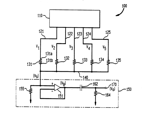
FIG. 1. shows a memory circuit 100 that operates
according to the present invention. The memory circuit
comprises a read signal source 110, a row of five memory
cells or resistors 131 through 135 and a readout circuit
150. It will be understood that the memory circuit 100 is
given by way of example only, and the use of an example
consisting of five memory cells is chosen to illustrate
the operation of the invention. The methods and
principles of the circuit 100 may readily be extended to a
2154~2
-
circuit consisting of a substantially greater number of
memory cells by those of ordinary skill in the art, and it
is well understood that a typical memory device may
include many thousands of bits. An example of a larger
scale memory device operating in accordance with the
principles of the present invention is discussed below in
connection with FIG. 10.
The elements of the memory circuit 100 are preferably
integrated onto a single semiconductor substrate. The
read signal source 110 includes five outputs 121 through
125 and may suitably comprise the circuit described below
in connection with FIG. 3. Each of the outputs 121
through 125 is connected to the first terminal of one of
the five memory resistors 131 through 135, such that the
first output 121 is connected to the first resistor 131,
the second output 122 is connected to the second resistor
132, and so forth. Each resistor has two terminals, such
as terminals 131a and 131b in the resistor 131. The
resistors 131 through 135 may be implemented as any
resistors suitable for use in an integrated circuit, such
as thin-film deposited resistors or ion-implanted
resistors. The resistive values typically range from 100
kn to 20 Mn, the particular resistance value being
representative of the information or data value that is to
be stored in the cell. For example, a 100 kQ resistor
represents one data value, a 400 kQ resistor represents
another, and so forth.
Each of the second terminals of the memory resistors
131 through 135 are commonly connected to a sum line 140.
The sum line 140 is connected to the readout circuit 150
which includes to both a load resistance 155 and a read
out circuit comprising a buffer 151 having an input and an
output, a capacitor 162 and a resistor 164. The sum line
140 is connected to one input of the buffer 151. The
buffer 151 may suitably be a high input impedance unity
2~8~2
-
gain buffer. The load resistance 155 is preferably much
larger in resistance value than the memory resistors 131
through 135. In fact, the load resistance 155 may
suitably comprise the internal input impedance of the
buffer 151. The output of the buffer 151 is connected
through a capacitor 162 to the circuit output 170. A
resistor 164 is also connected from the output 170 to
ground, thereby forming a differentiator circuit with the
capacitor 162. The capacitor 162 and resistor 164 should
be chosen such that the time constant of the
differentiator circuit, TDIPF~ is 1/6(~) to 1/lO(r) where ~
is the ramping period of the ramp step signals produced at
outputs 121 through 125.
In operation, the read signal source 110 preferably
provides at its five outputs 121 through 125 a sequential
series of read signals in the form of ramp step signals.
A ramp step signal is a voltage signal that starts at a
low voltage level, then increases as a function of time
until a step voltage level is reached, at which level it
remains thereafter. The ramp step signal sequence
appearing across the outputs 121 through 125 is shown in
FIGs. 2(a) through 2(e), respectively. The ramping period
T iS the time period during which the signal increases or
ramps to the step voltage level. The step voltage level
may suitably be 5 volts, and the ramping period may
suitably be 10-30 nanoseconds. As shown in Figs. 2(a)-
2(e), during a ramping period, each of the ramp step
signals V1 through V5 increases linearly at a rate S,
which is equal to the step voltage level divided by the
ramping period.
During the ramping period of the first ramp step
signal V1, a current flows through the memory resistor 131
to the sum line 140 and continues through the load
resistor 155 and the remaining memory resistors 132
through 135. The memory resistor 131 thus creates a
- 215~02
voltage divider with respect to the load resistor 155 and
the other memory resistors to produce a divided voltage,
VS, on the sum line 140. VS is given by the equation
Rl-3ll + Rl-3l2 + Rl-3l3 + Rl-3l4 + Rl-3l5 + Rl-5l5
It is to be noted that, for example, the resistance of the
resistor 132 is given by the variable Rl32, and other
component values are represented in a like fashion. If a
constant K is defined as
K=
Rl-3ll + Rl3l2 + Rl3l3 + Rl3l4 + Rl3l5 + Rl5l5
then VS becomes
VS = ( 1 )KVl
The voltage Vl during its ramping period may be expressed
as the function St. As a result, during the ramping
period of Vl, the sum line voltage VS comprises a ramp
signal that is proportional to the ramp voltage Vl from
the output 121. (See FIG. 2).
VS = ( 1 )KSt
The buffer 151, because it provides unity gain in the
present embodiment, produces a voltage VB at its output
which is substantially equivalent to the voltage VS. The
buffer 151 may alternatively provide gain if a higher
output level is desired. In any event, the resulting ramp
voltage VB is then differentiated by the capacitor 162 and
resistor 164, producing a more or less flat voltage level
output. The resulting output voltage V0 is shown in the
first segment 201 of FIG. 2(g). As stated previously, the
2 1~ 2
capacitor 162 and resistor 164 are chosen such that the
time constant, TDIFF~ Of the differentiator is 1/6(r) to
1/lO(r). The flat voltage level VO produced during the
ramping period of V1 is
VO =~R )KSTDiff -
At the time when the voltage V1 reaches the step
voltage level, the second output 122 produces the second
ramp step signal, beginning with its ramping period
signal. The current on the sum line 140 is then equal to
the sum of the current due to V1 and the current due to
V2. The component of the sum line current due to V1 is
constant because of the flat characteristic of V1, as seen
in FIG. 2(a), after the $tep voltage is reached. The
component of the sum line current due to V2, however,
ramps while V2 is in its ramping period.
As a result, the rate of change of VS is proportional
to the rate of change of V2, which should be equivalent to
S, or in other words, the rate of change of V1. For the
signal V2, Rl32 creates a voltage divider with respect to
the load resistor 155 and all of the remaining resistors.
As a result, the changing component of VS is given by
(R132)
where the constant K is the same as described before, when
V1 provided the rising voltage.
~ The buffer 151, as above, then produces a voltage VB
that is substantially equivalent to the voltage VS. The
resulting voltage VB is then differentiated by the
capacitor 162 and resistor 164, producing a more or less
flat voltage level output, which is shown as segment
corresponding to the time period 202 in FIG. 2(g). The
2~5~8~2
-
- 10 -
flat voltage level VO is produced during the rising
portion of V2 is
( Rl3 2 )
It is to be noted that because V1 is in a steady state
while V2 is ramping, V1 provides no component to the
differentiated voltage. Thus, VO, at distinct segments,
is proportional to the value of only one of the two memory
resistors 131 and 132. (See FIGS. 2(a), 2(b) and 2(g)).
Thereafter, the remaining outputs 123, 124 and 125
provide, in sequence, ramp step signals of the same shape
as V1 and v2. See Figs. 2(c), 2(d) and 2(e) for diagrams
of V3, V4 and V5, respectively. Each of the outputs 123,
124, and 125 provides the output ramp step signal at the
time when the voltage from the previous output reaches the
step voltage level. In this manner, the current and
therefore the voltage VS increases or ramps due to the
ramping current flowing into the sum line 140 from only
one of the memory resistors 131 through 135 at any one
time. As a result, the differentiated signal at VO
reflects the contribution of one memory resistor at each
segment. The value of each memory resistor may thereby be
ascertained, which provides the contents of the memory
circuit 100.
FIG. 2(f) shows an exemplary waveform of VS wherein
the resistance value of memory resistors 131 through 135
may suitably be 1.66 Mn, 2.5 Mn, 1.25 Mn, 2.5 Mn, and
1.25 Mn, respectively. The waveform VS comprises a
plurality of segments corresponding to each of the time
segments 201 through 205. The voltage on the sum line
140, or more particularly, the change in sum line voltage
reveals the memory contents. The read out circuit 150
then transforms the output to a more convenient form.
FIG. 2(g) shows VO produced by the read out circuit 150.
21 54 8D2
The memory resistors 131 through 135 produce output
voltage levels of 3x, 2x, 4x, 2x and 4x Vdc, respectively,
on segments 201 through 205, respectively. The value x is
a constant that is dependent upon the value of S and the
biasing voltages for the circuit. The memory resistors
131 through 135 may suitably represent the values 3, 2, 4,
2 and 4 stored in the memory. Given the present accuracy
of integrated circuit resistor values, data values may
readily be scaled to three decimal places of resolution.
Thus, for example, each resistor may store a numerical
value between 1 and 300. With future improvements in
integrated circuit fabrication technology, further
resolution would be attainable.
The present invention as incorporated in the above-
described example thus provides a novel memory circuit
configuration wherein a plurality memory cells comprise
passive impedance elements. In contrast, prior art
memories employ an active element such as a switch or a
transistor in each memory cell to isolate each of the
memory cells when it is being read out. Moreover, the
present invention is especially suited for memory cells
where the data value is represented by a passive impedance
value. In the circuit discussed above in connection with
FIG. 1, each memory resistor may store a data value having
three decimal places of resolution, for example, integers
between 1 and 300. Such resolution provides each cell
with the equivalent of on the order of 8 bits of binary
information.
FIG. 3 illustrates further details of one embodiment
of the read signal source 110 including five outputs 121
through 125 for providing a sequence of ramp step signals
suitable for use in the circuit 100 illustrated in FIG. 1.
The read signal source 110 comprises five delay buffers,
200, 220, 240, 260 and 280, each having an input and an
output. The five buffers 200 through 280 are connected in
21~48~2
series. The use of the phrase "connected in series" when
applied to a group of two or more circuit blocks herein
means that the input of each block is connected to the
output of the previous block, except for the first of such
blocks.
It is to be noted that while the detailed structure
of only the buffer 200 is shown and discussed below, the
remainder of the buffers 220 through 280 comprise the same
structure. The delay buffer 200 comprises an input 202
and an output which serves as the first output 121 of the
source 110, and two identically structured inverter
circuits connected in series. The first inverter circuit
includes a pFET 203 and an nFET 204 connected in a manner
well known to produce an inverter, and the second inverter
circuit includes a pFET 213 and an nFET 214 connected in a
manner well known to produce an inverter. Both inverters
are biased by a 5 Vdc bus and a ground bus.
Prior to application of a clock signal, 0 Vdc is
present at the input of the first inverter, the inverter
formed by FETs 203 and 204. Thus, the output of the first
inverter is 5 Vdc. This 5 Vdc output then appears at the
input of the second inverter, formed by FETs 213 and 214.
The output of the second inverter, which is also the
output 121 of the buffer 200, is then 0 Vdc with respect
to ground. Likewise, the second buffer 220, having the
same structure as buffer 200, also produces an output of 0
Vdc at its output 122. The buffers 220, 240, 260 and 280
similarly produce 0 Vdc at their outputs 123, 124 and 125
respectively.
In operation, a ramp step clock signal is provided by
a system clock 210 to the input 202 of the first inverter
of the first buffer 200. The ramp step function is chosen
such that approximately 1/2 the step voltage equals the
threshold of the first inverter. A suitable system clock
operable to provide such signals would be known to those
- 13 -
of ordinary skill in the art. At the time the clock ramp
signal reaches the first inverter threshold voltage, the
first inverter output starts to transition towards the low
voltage level, or in other words, its voltage starts to
drop towards 0 Vdc. The voltage at the output of the
first inverter does not drop instantaneously, however, due
to the parasitic capacitance inherent in the physical
structure of the FETs 203 and 204. The rate at which the
inverter output voltage decreases is referred to as the
slew rate.
It is known that the slew rate of an inverter may be
controlled by manipulating the geometry of its component
FETs. The FETs 202 and 203, and, indeed, the FETs in all
the buffers 200 through 280, are fabricated identically in
a way such that the slew rate of the inverter causes the
transition between 0 Vdc and 5 Vdc, or the reverse, to be
equal to the ramping period of the output read signals, V1
through V5. It is known that by increasing the FET's
physical length of the FET, its transition time may be
increased. For example, in a silicon-based MOSFET, a 1
micron FET transitions from 0 to 5 Vdc in approximately 1
nanosecond while a 3-5 micron FET transitions from 0 to 5
Vdc in 5-10 nanoseconds. Furthermore, a 10 micron FET
transitions from 0 to 5 Vdc in 20-30 nanoseconds. The
details of the fabrication of these and other types of
FETs having the proper slew rates are known to those of
ordinary skill in the art.
Returning to the description of the circuit's
operation, after the first inverter slews downward for
approximately 1/2 the ramping period, the first inverter
output reaches the threshold voltage of the second
inverter. When the threshold is crossed, the second
inverter output 121 will change from 0 Vdc to 5 Vdc,
subject again to its slew rate. The second inverter
formed by the FETs 213 and 214 produces a signal as shown
215q~2
-
in FIG. 4(b). To summarize, the delay buffer 200 doubly
inverts the clock signal, and the combined slew rates of
the first and second inverters provide a delayed ramp step
signal, V1, as illustrated in FIGs. 4(a) and 4(b).
The second buffer 220 operates in a similar manner,
however, instead of receiving a clock signal at its input,
it receives the delayed ramp step signal of the first
buffer 200, V1. A doubly inverted and delayed ramp step
function as shown in FIG. 4(c) thereafter appears at the
output 122 of the second buffer 220. The remaining
buffers 240, 260 and 280 operate in like fashion,
providing V3, V4 and V5 as shown in FIGS. 4(d), 4(e) and 4
respectively to outputs 123, 124 and 125, respectively.
FIG. 5 shows an alternative embodiment of the memory
circuit device according to the present invention wherein
the five memory cells comprise five capacitors 331 through
335, and the value of the capacitance represents the
information stored within the cells. The circuit in FIG.
5 may suitably employ the same read signal source 110 as
discussed above in connection with FIG. 1.
In the embodiment of FIG. 5 the outputs 121 through
125 of the read signal source 110 are each directly
connected to a first terminal one of five memory
capacitors 331 through 335, such that the first output 121
is connected to the first capacitor 331, the second output
122 is connected to the second capacitor 332, and so
forth. Each of the capacitors 331 through 335 have two
terminals, such as terminals 331a and 331b of the
capacitor 331. The capacitance values typically range
from .01 pF to .1 pF, where the particular value depends
upon the information value stored in a cell. For example,
a .01 pF capacitor represents one data value, a .015 pF
capacitor signifies another, and so forth.
The second terminal of each memory capacitors 331
through 335 are further connected to a sum line 338. The
~ls~a~2
-
sum line 338 is coupled to a read out circuit 339
comprising a buffer 350 and a resistor 340. The resistor
340 forms a differentiator circuit with the bank of memory
capacitors 331 through 335. The differentiating resistor
340 should be chosen low enough such that the time
constant of the circuit, R340 (C331 + C332 + C333 + C334 + C335),
is equal to 1/6(~) to 1/10(~) where, again, I is the
ramping period of each of the signals Vl through Vs~ The
buffer 350 may suitably be a high gain buffer. The buffer
350 is further connected to the circuit output 360.
In operation, the read signal source 110 provides at
its outputs 121 through 125 a sequence of ramp step
signals Vl through V5 in substantially the same manner as
discussed above in connection with FIG. 1. FIGs. 6(a)
through 6(e) show the signals Vl through V5. When signal
Vl begins to ramp, the memory capacitor 331 and the
differentiating resistor 340 differentiate the Vl signal.
The differentiated signal may be expressed as VS =
C33lR340 (dVl/dt). During the ramping period, dVl/dt is
equal to a constant value S. Therefore, in its first
segment, VS = C33lR340S. The remaining capacitors do not
significantly affect the signal on the sum line 338
because of the low value chosen for the time constant R340
( C331 + C332 + C332 + C334 + C335 ) -
When V2 begins to ramp, Vl becomes constant, causing
the capacitor 331 to create a passive, steady state
circuit between the first output 121 and the rest of the
circuit. As a result, the voltage or the sum line 338
will be influenced by only the ramping V2. The sum line
voltage equals the voltage V2 differentiated by R340 and
C332. As a result, the second segment of VS will then
equal C332R34oS-
Thereafter as the read signal source 110 provides theramp step signal to each of the outputs 123 through 125
sequentially, as shown in Figs. 6(a) to 6(e), the signal
`~ 21~4~02
- 16 -
VS exhibits a sequence of segments having voltage levels
that are proportional to the values of the memory
capacitors 331 through 335 as seen in FIG. 6(f). As was
the case in the circuit 100 illustrated in FIG. 1, the
output levels are indicative of the value stored within
the memory cell, although in this case such values are
represented by the capacitance values of the memory
capacitors 331 through 335. In the present embodiment,
the capacitance values may suitably represent a numerical
value between 1 and 20, where a .01 pF capacitor
represents a numerical value of 1 and a .1 pF capacitor
represents a numerical value of 20, with more or less even
intervals of .005 pF between adjacent values. Again,
future fabrication improvements would allow additional
intervals.
In another embodiment of the present invention, the
circuit in FIG. 5 is modified to operate with an
alternative read signal source 110. Instead of utilizing
a read signal source that is operable to provide read
signals in the form of ramp step signals, this alternative
embodiment employs a read signal source operable to
provide rectangular wave pulse signals. A rectangular
wave pulse signal consists of a signal that rapidly
transitions from a low voltage state to a high voltage
state, remains at the high voltage state for a
predetermined period, and then rapidly transitions back to
the low voltage state~ The sequence of rectangular wave
signals appearing at the source outputs 121 through 125 is
illustrated in FIGS. 7(a) through 7(e).
In the operation of the alternative embodiment of the
circuit in FIG. 5, the read signal source 110 provides at
its outputs 121 through 125 a sequence of rectangular wave
pulses. FIGS. 7(a) through 7(e) illustrate for the signal
waveforms appearing across the outputs 121 through 125.
For the particular embodiment described herein, the
2154~2
- 17 -
rectangular wave signals may suitably be 5 volts in
amplitude and have a duration of approximately 10-100
nanoseconds. A11 the pulses in the sequence should have
substantially identical amplitudes and periods.
When the first output 121 produces the first
rectangular wave pulse, the fast rise time of the pulse
provokes an impulse response from the capacitor 331, or
C331. For the impulse response, C331 creates a voltage
divider with respect to the remaining memory capacitors
C332 through C33s~ as well as the load resistor. The load
resistor 340, however, is chosen to be large enough that
it does not effect the impulse response. To choose the
proper resistor, the time constant of the circuit formed
by R340 (C331 + C332 + C332 + C334 + C335) should be at least 6
to 10 times the period of the rectangular wave pulse.
The resulting output voltage VS on the sum line 338
equals
C331 + C332 + C333 + C334 + C335
where ~ is the magnitude of the impulse in V1, which
equals 5 volts. If a constant K is defined as:
K =
C331 + C332 + C333 + C334 + C335
then the output voltage equals
VS = C331K~ -
For the remaining duration of the rectangular wave pulse,
the voltage VS remains substantially at the impulse
voltage due to the long time constant created by the large
340 -
The downward impulse then created at the end of the
rectangular wave pulse as shown in FIG. 7(a) causes VS to
tend to return to zero volts rapidly. During or after the
2154~0~
- 18 -
downward impulse of Vl occurs, output 122 provides an
upward impulse that signifies the beginning of another
rectangular wave pulse, now in V2. Again, the fast rise
time of V2 provokes an impulse response from the capacitor
332. In this case, the capacitor 332 creates a voltage
divider with respect to the remaining memory capacitors
331, 333, 334, and 335, and the load resistor 340. The
impulse response provides a sum line voltage of VS =
C332k8. As before, the voltage VS will remain
substantially at the impulse response voltage due to the
large time constant created by R340.
Thus, the voltage VS provides a sequence of signal
segments at voltage levels that are directly proportional
to the capacitance of each of the memory capacitors 331
through 335. The output voltage VO is then isolated from
the sum line 338 by the buffer 350. FIG. 7 illustrates an
example of the sum line voltage for a circuit where: Cs3
= .02pF; C532 = .0lpF; Cs33 = 0 3pF; Cs34 = . OlpF; and Cs3s =
.03pF. The data stored by such capacitance values is 4,
2, 6, 2 and 6, respectively.
An example of a suitable rectangular wave pulse
source 510 is illustrated in FIG. 8. The square pulse
source 510 may be used as the read signal source 110 in
the alternative embodiment of the circuit in FIG. 5. The
pulse source 510 comprises five propagating pulse buffers
581 through 585. The propagating pulse buffers 581
through 585 each include one of five output connections
521 through 525, respectively, which in turn may each be
connected to a distinct memory cell, such as the memory
cells 331 through 335 in FIG. 5. Although the propagating
pulse buffer 581 is shown and briefly described below,
further details regarding the operation of this circuit
may be found in M. Shoji, "Theory of CMOS Digital Circuits
and Circuit Failures," pp. 483-494 (Princeton Univ. Press
1992), which is incorporated by reference herein.
2~5~8~
- 19 --
The propagating pulse buffer 581 consists of an input
570 connected to a first inverter 5711. The first
inverter 5711 is further connected to a second inverter
5712, which in turn is connected to a third inverter 5713,
5 which in turn is connected to a fourth inverter 5714. The
output of the fourth inverter 5714 iS then connected to
the first source output connection 521. Each of the
inverters 5711 through 5714 comprises a well-known two FET
inverter structure, and each is connected to a +5 Vdc bias
voltage and ground. The propagating pulse buffers 582,
583, 584 and 585 comprise similar structures.
The pulse source 510 operates in the following
manner. A rectangular wave pulse clock signal is provided
at the input 570. The inverter 5711 provides a delayed,
15 inverted rectangular wave pulse signal, VA~ at its output
as illustrated in FIG. 9(b). The amount of delay is
determined by the inherent capacitance of the circuit
elements in the inverter. As was the case in the
inverters employed in the circuit in FIG. 3, the delay of
20 the inverter may be adjusted by manipulating the length of
the constituent FETs.
The inverters 5711 through 5714 should exhibit a rise
time of approximately 1/n the length of the pulse, where n
is the number of inverters per propagating pulse buffer.
25 It should be noted that attempts to reduce the number of
circuit elements by reducing the number of inverters per
buffer may compromise ability of the pulse to propagate
through the circuit. In fact, in order to decrease the
rise time of the output pulse while maintaining the pulse
delay, fast inverters should be used, and the number of
inverters per buffer should preferably be increased to 6
or even 10. The improved rise time elicits a better
impulse response from the memory circuit capacitors 531
through 535.
21~48~2
- 20 -
Each of the above examples illustrate the method of
the present invention applied to one row of five memory
cells. Practical applications, however, may require
substantially more than five memory cells. To this end,
the principles discussed above may readily be applied to
large scale memory circuits.
As an initial matter, it should be noted that on the
order of forty memory cells, either memory resistors or
memory capacitors, may be accommodated by the single row
structures in FIGS. 1 and 5. For example, in FIG. 1,
there may be forty outputs, similar to the outputs 121
through 125, connected to forty memory resistors. The
memory resistors are all connected thereafter to the sum
line 140 and the read out circuit.
Furthermore, several of such rows of memory cells may
be integrated together, each row associated with its own
sum line. The several sum lines may then be selectively
enabled, one at a time. An example of such a circuit is
illustrated in FIG. 10 and described below. FIG. 10 shows
a memory circuit 600 consisting of 3 rows of 7 memory
cells. The number of cells is given by way of example,
and much larger memory circuits of on the order of 1,000
rows of 40 memory cells or, in other words, 40,000 cells,
may be readily implemented by those of ordinary skill in
the art. The elements of the circuit in FIG. 10 may all
be implemented on a single integrated circuit.
Furthermore, a suitable read signal source may also be
integrated into the circuit to reduce the external
circuitry required.
The memory circuit 600 comprises seven output lines
6101 through 6107 that form a two dimensional matrix with
three sum lines 622, 632 and 642. The seven output lines
610l through 6107 are connected to a ramp step signal
source, not shown, which may suitably be of the kind
described in connection with FIG. 3, above. Each of the
21~4~2
output lines 6101 through 6107 is connected to a distinct
resistor of the first row of memory resistors 6201 through
6207. The memory resistors 6201 through 6207 are further
connected to the sum line 622. Likewise, each of the
output lines 6101 through 6107 is connected to a distinct
resistor of the second row of memory resistors 6301
through 6307 the memory resistor 6301 through 6307, are
further connected to the sum line 632. Finally, each of
the output lines 6101 through 6107 is further connected to
a distinct resistor of the third row of memory resistors
640l through 6407. The memory resistors are further
connected to the sum line 642.
Each of the sum lines 622, 632 and 642 is connected
to a distinct read out select switch of three switches
624, 634 and 644. The switches 624, 634, and 644 connect
the sum lines 622, 632 and 642, respectively to the read
out line 650. The read out line select switches 624, 634
and 644 are further operably connected to one of three
select lines 626, 636 and 646, respectively. The read out
line 650 is connected to a read out circuit 655 comprising
a buffer 660, a capacitor 672 and a resistor 674. The
read out line 650 is connected to the input of the buffer
660. The buffer 660 is thereafter connected to a
differentiator circuit created by the capacitor 672 and
the resistor 674.
The contents of the memory circuit illustrated in
FIG. 10 may be sequentially read out in the following
manner. In general, the memory resistors 6201 through
6207, 6301 through 6307 and 640l through 6407 are read row
by row, in sequence. To this end, only one of the sum
lines 622, 632, and 642 is enabled at one time. When a
particular sum line is enabled, the memory resistors
connected thereto are read out in a manner similar to that
described in connection with the operation of the circuit
in FIG. 1.
215480~
- 22 -
To read out the first row of memory resistors, an
enable signal is provided to the first read out select
switch 624 through the select line 626. The enabled
select switch 624 allows current to flow from the first
sum line 622 to the read out line 650. Once the sum line
622 is connected to the read out line, a sequence of ramp
step signals is provided to the outputs 6101 through 6107
in the same manner as described above in connection with
FIG. 1. The read out circuit 6S5 then provides a multiple
segment output signal, each segment corresponding to one
of the ramp step signals provided at the outputs 6101
through 6107 and indicative of the resistance value of the
resistors 6201 through 6207 in a similar manner as the
circuit described in connection with FIG. 1, above. When
the first row has been read out, the enable signal is
removed from the first select switch 624. An enable
signal is then provided to the second select switch 634
through the select line 636, and the second row is read
out in the same manner as the first. After the second row
is read out, the third row is enabled and read out.
It is to be understood that the above-described
embodiments of the invention are merely illustrative.
Other implementations may readily be devised by those
skilled in the art which will embody the principles of the
invention and fall within the spirit and scope thereof.
For example, while exemplary embodiments are disclosed
using resistors and capacitors as memory cells, other
passive impedance devices such as a diode may be used.
The impedance characteristics of a diode are nonlinear,
but nevertheless may be adjusted to correspond to
different data values by manipulating doping levels. The
resulting nonlinear resistance values may then represent
data store within the memory.