Note: Descriptions are shown in the official language in which they were submitted.
0 94/l8687 PCT/US94/00349
APPARATTJS AND ~13THOI) FOR YWl'l'l_'~llNG HIGH POWER
FTT~T.n OF THE INVENTION
This invention relates to switching high power levels, and
more specif ically to circuits and procedures for such
5 switching using series-coupled devices, including semicon-
ductor devices.
BACKGROUND OF THE INVENTION
In many high power applications it is n~oc~oRs~ry to switch
high voltage and high current levels. For example, a power
0 utility company must ~requently provide high potentials
(e.g., many kV) to avoid having to provide ~ bly
large current levels ~e.g., hundreds or th~ cFIn~1c Of
amperes). Further, if high potentials can be suitably
switched, it is often pos8ible to operate equipment directly
15 ~rom the alternating current high di3tribution lines,
without the cost of providing a suitable transformer.
It is known in the art to use series-coupled thyristors to
switch high voltage levels, especially at distribution line
potentials. Thyristors are three terminal devices that have
20 high voltage and high current ratings, but unfortunately do
not turn-off in response to a signal applied to the device
gate input terminal. Once turned on by a gate current input
3ignal, thyristors remain latched in the on state until the
signal at the output ~ n;~l ~ is interrupted, thus
25 permitting the thyristor to turn off. For this reason,
.. _ . , . , .. . .. . . . _ ... . . . . . .. _ _ _ _ _
W094/l8687 2~55l~a PCI/US94100349
thyri6tors are typically used in power converter applica-
tions where commu~ation occurs naturally. In a natural
commutation ~pplication, if a second device is turned on
before a first deYice is turned off, it is understood that
5 current from the irst device will automatically be diverted
to the second device, whereupon the f irst device turns of f .
However, thyristors are not preierred in inverter or pulse
width modulation applications because of .the complex (and
power ~ nCl~~; n~ y commutation ci;rcuitry reqLIired to
10 forcibly commutate or properly turn off - the devices.
. ~
More rece~tly, gate turn-of f thyristors ( "GTOs" ) have been
used in high potential switching applications where natural
con~mutation does not occur. A GTO is a three terminal
device somewhat sirnilar to a conv~ont;~n~l thyristor, except
5 that the GTO can turn off in response to ~i typically large
current signal at its gate input terminal. GTOs are
commonly used irl traction applications to implement airect
current choppers, and GTOs have been propo8ed f or use in
static condenser applications and energy storage schemes.
20 Like thyri8tors, GTOs have a relatively low intrinsic dV/dt
limitation (e.g., 500 V/~s) that requires external compo-
nents to ensure that the rate of voltage change across the
device af ter turn of does not exceed the limitation .
Typically large snubber capacitors (e.g., 5 IlF) are used for
25 this purpose, but un~ortunately dissipate considerable
energy, and li~Lit the practical switching frequency of
circuits using GTOs. Essentially, whatever energy is stored
in the snubber capacitor after turning pff the GTO is dissi-
pated when the device is next turned on. Thus, f or each
30 off-on GTO cycle, one ~quantum~' of snubber energy is
qi~ d, and attempting to increase the GTO switching
rate beyond say 180 Xz increases the snubber~ losses to an
unacceptable level.
A8 such, GTO8 are not useful for applications, where, for
35 example, a high switching frequency is desired to reduce low
order harmonic di6tortion of the voltage or current
~jO 94/18687 2 ~ ~ ~10 ~ PCTIIJS94/00349
--3--
waveform. For the same reason, it i8 difficult to construcl
a fast pulse-width rlcrl~ ted inverter using GTOs for
operation directly from high voltage alternating current
lines, for example, to form an active filter and volt-ampere
5 reactive ( ~var'~ ) compensator.
In high voltage, high-current switching applications,
several deviceæ (thyristors, GTOs, and the like) are
series-coupled such that the voltage across any one device
i9 less than the device breakdown voltage. Understandably
it is important that the high voltage be dynamically shared
among the series-coupled devices during turn-on and turn-off
transitions .
While each serie8-coupled device may experience the same
differential high voltage potential, devices coupled at the
"top" of the series are at a higher absolute potential
compared with devices coupled at the "bottom~ of the series.
Because of the higher absolute voltage potentials seen by
the devices nearer the ~top~ of the series, it i8 often
difficult to safely provide proper gate drive signals to the
2 0 various devices . For the same reason, the generation of
power to operate the various gate drive circuits can also be
troublesome .
What is needed is an apparatus and method_ ~or saf ely
switching high voltage at high current levels, especially in
2~ applications where natural commutation need not occur.
Preferably such apparatus and method should operate using
series-coupled three terminal devices, which devices are
commercially available, self---~nt;linP~ and modular.
Further, such apparatus and method should not require
3 0 snubbers with their OEcessive power dissipation and high
frequency 8witching limitations.
In addition, there is a need for a means to modulari7e each
series-coupled device and its associated circuitry, and to
provide safe isolation from high voltage potentials seen by
WO 94/l8687 2 ~ 5 ~ 10 ~ PCT/US94100349
the various devices. Finally, the gate drive circuitry used
to drive such devices preferably should derive operating
power from the high voltage seen by each device, and dynamic
voltage sharing should be ensured among the various
series-coupled deYices. The present invention discloses
such an apparatus and method fulfilling, these needs.
SIJMMA~Y OF T~ pR~NT INVENTION ~
The present invention provides an apparatus and method f or
switching high power levels, using series-coupled devices
10 that preferably are voltage controlled gate turn-off devices
( "VCGTO" ) such as insulated gate bipolar transistors
( " IGBT" ~, metal-oxide-~ilicon ( "MOS" ) controlled thyristors
("MCT"), or power metal-oxide-silicon field effect
transistors ("MOSFETS"). Unlike GTOs, VCGTO devices
15 advantageously have subst~nt; ~11 y no dV/dt limitation, and
may be used in high ~requency applications (e . g ., switching
rates in the 2 XHz to 10 KE~z range) as no heat dissipating
snubbers are required, and ;nt.ornAl switching losses are
small .
20 Preferably each VCGTO and its associated circuitry forms a
module, where a number (N) of such identical modules are
series-coupled between the high voltage rails to be
switched. Each module include6 an input port for receiving
a gate drive sicJnal, input interface and gate drivi~g
25 circuitry, a VCGTO device having a gate input terminal and
first and second output terminals, two power switching ports
coupled to the output tPrm; n~ of the VCGTO device, and a
clamping m~.hz~n; ~m and regulated clamp voltage circuit
coupled across the VCGTO device output tf~rm; n~l Fl,
30 The input interface and gate driving circuitry receives a
gate drive signal that is preferably optically coupled and
provides a corresponding voltage input signal to the gate of
the VCGTO device.
O 94/18687 2 ~ PCT/US94/00349
-5-
The clamping mechanism and regulated clamp voltage circui~
are coupled across the output terminals of the VCGTO device
to clamp the first (high potential) output terminal of the
device to a potential det,-rm; netl by the regulated clamp
5 voltage circuit. As such, the maximum differential
potential between the output terminals of the VCGTO device
is ~-;nt~ined under all conditions at a predetermined safe
level, well within the breakdown voltage rating of the
device. The regulated clamp voltage circuit derives its
lO operating potential from the high voltage switched by the
associated VCGTO device. The regulated clamp voltage
circuit also provides from this derived potential a
regulated low voltage potential that operates the associated
input interface and gate drive circuitry. In this fashion,
15 the module is self-c-~nt~;n~d and derives its own operating
power from the high potential to be switched.
Preferably each module is identical, as is each device.
Thus, any non-simultaneous switching of the various devices
in the series-coupled modules causes only a slight disparity
2 0 in the amount of energy absorbed by each regulated clamp
voltage circuit. Because each module is identical and sees
substantially the same differential potential between the
module output ports, the modules operate i~dependently
regardless of where in the series-coupled chain they are
25 located. Thus, apart from mechanical considerations, as
many modules as desired may be series-coupled between the
high potential rails to form a single switch or valve.
As such, a valve according to the present invention is
assured of dynamic voltage sharing among the various
30 modules, and may be operated at a relatively rapid switching
frequency, as no snubber is required. Finally, because the
devices are preferably VCGTOs, the invention may be used in
applications where commutation does not occur naturally.
In a second aspect, a method of switching high voltage at
35 high current using series-coupled devices is disclosed. The
WO 94/18687 2 ~ 5 ~ ~ a ~ 6 - PCT/US94/00349
method requires_=serie5 coupling a stack of preferably
identical modules, each module containing a three terminal
device, an isolated drive --~~h_ni Ant for controlling the
device in response to an input signal, and a regulated clamp
5 voltage ~--h_n; ATTI coupled across the device' 8 output
terminals, wherein operating potential for the two
me~-h;-ni I is derived from the high voltage potential
switched by the device
Other features and advantages of the invention will appear
l0 from the following description in which the preferred
emboA; - A have been set forth in detail, in conjunction
with the ~crn~r_n~ing drawings.
RRT~- DEsrRTpTIoN OF THE DRAWINGS
FIGURE l depicts a valve for safely switching high voltage
15 at high current using series-coupled modules, according to
the present invention;
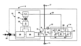
FIGURE 2 is a schematic representation of a module, ac-
cording to the present invention;
FIGURE 3 i9 a sc11ematic repre8entation of a high voltage
20 pulse width modulator using valves, according to the present
invention;
FIGURES 4A and 4B depict voltage and current waveforms, as
seen by a valve ' n the embodiment of FIGI~RE 3 .
DETAII.ED DESCRIPTION OF THE PREFERRED EMBODIMENT
25 Figure l depicts a valve apparatus according to the present
invention as preferably including several self-cnnt~;n~
modules 2, coupled in series between an upper potential rail
4 and a lower potential rail 6 to form a high voltage
switching valve. Preferably each module 2 is identical and
30 includes a three t~rmin_l solid state~switch device 8, an
~O 94118687 2 1 5 510 ~ PCTIUS94/00349
input interface and drive mechanism l0, a clamp mechanism
12, and a regulated clamp voltage source 14. Each module
has an upper and lower ~lectrical port, respectively denoted
U and L, and an input port I for receiving an input signal
5 (shown by dashed arrow) that causes the switch to turn on
and of f .
When the valve is switched on, all modules pass a current
that flows from rail 4 to rail 6, and when the valve is
switched off, this current is blocked. Depending upon the
l0 application, rail 4 may be, for example, the power source,
and rail 6 may be the output terminal of the valve
apparatus .
The drive mechanism l0 is coupled between the input port I
and the input terminal G of the switch device 8. Preferably
15 the switch device 8 is a voltage controlled gate turn-off
device ("VCGTO") such as an insulated gate bipolar
transistor ("IGBT") or a metal-oxide-silicon controlled
thyristor ( "MCT" ) . As noted, such devices have essentially
no dV/dt limitation and thus do not require an energy
20 dissipating snubber. The switch device 8 has a first output
terminal coupled to the upper port U, and a second output
terminal coupled to the lower port L. For example, device
8 may be a 300 ampere, 1.2 kV IGBT, such as a Toshiba
MG300QllJSl, a device having an essentially unlimited dV/dt
25 rating.
Collectively, the clamp -~~h;~nl rm 12 and regulated clamp
voltage source 14 are coupled across the output t~rmin~s of
device 8, and ensure that the maximum differential Yoltage
appearing across the output t~rm; n;ll s is ~ithin the maximum
30 breakdown voltage.of device 8. As depicted in Figure l, the
regulated clamp voltage source 14 derives its operating
potential from the switched potential appearing across the
device output terminals (or the U and ~ output ports), and
provides from this derived potential operating voltage for
35 the drive -^ch: ni ~m l0 . Operating potential for the
_ _ _ . . , . . _ _ . .. . . _ _ _ _
WO 94118687 PCTIUS94/00349
2~i5la~ -8-
regulated clamp voltage source 14 (and thus for drive
m~ h;ln; ~m 10 as well) is agsured. This is true even during
initial system turn-on, providing that the valve blocks full
rail-to-rail Yoltage whenever the valve is switch off.
5 Flgure 2 depicts in greater detail the c~ non~-ntq comprising
module 2. ~ccording to the present invention, the potential
difference between rails 4 and 6 may be many thousands of
volts, at a current level of tens or hundreds of amperes,
and the potential difference between a module' s U and L
l0 output ports may be a thousand volts or so. It is
understood that if the potential difference between rails 4
and 6 is, say, 20 kV, and if the maximum voltage a module 2
can safely sustain between its ports U and ~ is-only 1.2 kV,
that the number ~N) of modules 2 that will be series coupled
15 will be 20/1.2 or 16.7, e.g., 17 modules or more. Typically
more than N modules will be used, to provide safety margin
and rPr~llnll~n~y
For safety and isolation ~nqirl~rations, preferably the
input signal (depicted by dashed arrow) is coupled to the
20 input port I of device 2 via a fiber optic cable 20. T~e
input signal is essentially a train of ~on~ and "off"
pulses, whose switching frequency preferably is in the range
of about 3 KHz to about l0 ~Hz, and a duty cycle essentially
variable from zero to l00~6. The input signal typically is
25 provided, via fiber optic cable 20, by a main control
circuit (not shown).
As depicted in ~igure 2, drive mechanism l0 preferably
includes an optical receiver 22 whose output is electrically
coupled to a gate drive circuit 24 whose output is floating.
30 Operating potential for receiver 22 and circuit 24 is
provided by a DC-DC converter comprising oscillator 26,
isolation trans~ormer 28 and a low voltage "E~" bridge
rectifier 30. The use of such a DC-DC co~verter with
transformer isolation permits circuit 24 to deliver a
35 bipolar drive voltage signal to the input gate terminal G of
~WO 94/18687 2 ~ ~ 5 1 ~ ~ PC~/US94100349
device 8. Preferably this drive signal is about t 15-V
relative to the potential at output port ~) and replicate6
the input signal received at the input port I. Of course
alternative circuitry may be employed to provide a suitable
5 signal to input gate terminal G. While a bipolar input gate
signal is not required to control device 8, preferably a
bipolar drive signal is used to minimize spurious control of
device 8 due to voltage coupling through stray capacitance
between the output port L and the device gate terminal G.
10 Diode D1 is typically integrally mounted within the device
8 package to provide protection against reverse voltage
across output ports U and L, by providing a safe path for
current flow from port L to port U. Diode 12 performs a
clamping function, preventing the output port U's potential
15 from rising substA~ti~lly higher than the potential at the
upper lead of capacitor Cl. Preferably capacitor C1 is
implemented as two capacitors in parallel, a relatively
small capacitor (e.g., 0.1 ~lf) and a larger capacitor (e.g.,
15 uF) . Two capacitors are preferably used to implement C1,
20 to minimize voltage drop in the current loop comprising
diode 12, capacitor C1 and device 8 (which ;nrl~ q diode Dl
ln~rnAlly) due to unavoidable resistance and inductance.
The smaller 0.1 ,uf capacitor can be mounted more intimately
to device 8 and diode 12, while permitting the larger
25 capacitor to be mounted several inches (e.g., 5 cm or so)
distant . Of course the voltage rating f or the capacitors
comprising C1 should exceed the highest differential
potential to which output ports U and L will be exposed,
e . g ., about 1 kV .
30 Regulated clamp voltage source 14 ;nrllldf~q capacitor C1,
which charges positively toward the potential present at
output port U when device 8 is turned of f, and a clamp
voltage regulator circuit 34 that senses (via a resistor
divider chain 36) and stabilizes the potential across
35 capacitor C1. The output from circuit 34 is coupled via
lead 38 to the input of a smaller IGBT or MCT device 40.
WO 94/l8687 21$ ~ 10 0 - lo - PCT/US94/00349
commercially available 8 amperer 1.2 kV IGBT may be used fcr
device 40, although many applications reSIuire le8s than one
ampere to be conducted by device 40.
When device 8 is turned on, the voltage di~erential between
5 output ports U and L i9 essentially ~ zero . The voltage
across capacitor C1 will tend to remain constant, as diode
12 is now reverse biased. In practice the potential across
Cl is maintained at a level less than the breakdown rating
of device 8, and is typically about 800 V, where device 8 is
10 rated at about 1.2 kV. This allows a com~ortable margin to
ac~ . ' te parasitic transient effects due to stray
;n~ rtcnC~ a8sociated with the clamp ch~n;~m
However as device 8 turns off (in response to a signal at
the i~put port I), the current through device 8 falls
15 rapidly, and the current ~lowing from output port U begins
to divert through diode 12 into capacitor C1. Capacitor C1
is su~iciently large that for typically several
micros~c~ n~lc there is no appreciable change in voltage
across C1. The potential at output port U at this time is
2 0 about one diode drop ~ e . g ., diode 12 ) higher than the
potential at the top of C1.
By design, this potential exceeds the potential in the main
power circuit by about 2096, thus causing the main circuit
load current through this module to decrease rapidly. As
25 will be apparent in the particular application depicted in
Figure 3 (to be described), the main power circuit current
that had been ~lol~ing through thi~s module ~ ~ ~t~s around
the system DC link capacitor, and flows through the
corresponding diode~ Dl in the opposing ~Lodule arm in the
30 same pole. This commutation takes place rapidly, perhaps
over a 1 ~18 irLterval, at the end o~ whick interval the
current f low through diodes 12 and capacitor C1 is reduced
to nil . As device 8 turns of f, the current ~low through
capacitor C1 rises rapidly f rom zero to the peak current
~0 94118687 2 1 5 ~ I O ~ PCT/US94100349
that had been flowing through device 8, and then falls
zero quickly.
During typically 5everal of these 1 IlS or 80 intervals, the
potential at the top of Cl begins to rise, as does the
5 differential voltage between output ports U and L, during
turn-off. When the differential potential across capacitor
Cl exceeds a predetermined maximum level (typically about
800 V) determined by circuit 34 and divider chain 36,
circuit 34 turns on the device 40. When turned on, device
lO 40 begins to discharge the potential across capacitor Cl,
via a 200 W or 80 current limiting series resistor R that
provides a substantially greater power drain from capacitor
Cl than the anticipated peak clamp power for each level of
module 2 comprising the overall valve.
15 When device 40 is turned on by circuit 34, Cl discharges
through resistor R until a lower threshold voltage is
attained, at which level circuit 34 turns off device 40,
allowing Cl to once again charge via diode 12 to the
potential at output port U. However, when the predetermined
20 maximum level is exceeded, circuit 34 again turns on device-
40, thus regulating the potential difference across
capacitor Cl, and thus across output ports U and L. In some
applications, the resistor chain 36 may itself be sufficient
to dissipate the bulk of the clamp 109s across capacitor Cl,
25 in which case device 40 is seldom turned on by circuit 34.
In practice, the dif f erence between the upper and lower
threshold levels a8sociated with the regulated clamp voltage
source 14 is easily held to a few percent of the maximum DC
voltage level appearing across output ports U and L.
30 Details of the clamp voltage regulator circuit 34 are not
provided as such circuitry is well known to those skilled in
the art of power supply design.
A low voltage zener diode 42 (e . g ., 15 V) and storage
capacitor 44 (e.g., 15 IlF) are coupled across capacitor Cl
35 via a current-limiting resistor to provide a regulated low
_ _ _ _ _ _ ~ _ , . . ....... . . .
WO 94/18687 2 ~ 5 ~ PCT/US94/00349
--12-
operating potential (e . g ., 15 VDC) that is coupled vi~ lead
32 to power the input interface and drive r~-hAn1~ lO.
E~ach module is self-contained with an optically coupled
input port I, with only two electrical connections to the
5 outside world (e.g., a U output port coupled to the L output
port of the module above it, and an ~ output port coupled to
the U output port of the modulé below it). A5 such, the N
modules comprising a valve function ;n~r~n~ntly of each
other, without knowledge of where in the series-coupled
10 chain of modules it is located. Thus, with reference to
Figure 1, although the uppermost module 2 is coupled to the
upper potential rail 4, and sees a higher absolute potential
relative to the lower potential rail 6 than the other
modules 2 see, it operates precisely as though it were the
15 lowermost module whose ~ output port was coupled directly to
the lower voltage rail ~.
Analysis of clamp diode 12 and circuit 14 ; nd; ("At~ that
clamp power d; ~iration is only about 150 W to 200 W per
module in an ~pp];cat;on wherein a 13.8 kV inverter is
20 switched at 3 kHz with 300 amperes peak current. Consid-
ering the relatively small amount of energy involved,
recovery of thi6 energy would require transformer8 and would
be impractical.
The valve design is not particularly dependent on the
25 switching characteristics of device 8, and does not require
special pr~r A1ltinn~ to ensure dynamic voltage sharing. The
above-described operation of diode 12 and circuit 14 hold
the differential voltage across each device 8 (e.g., across
output ports U and 1,) to a safe maximum level under all
30 conditions. As such, the only consequence of non-
simultaneous switching of series-coupled modules in a valve
is a slight disparity in the amount of energy absorbed by
diode 12 and circuit 14. In practice, however, the
switching characteristics of I~3B~ type devices 8 are su~fi-
35 ciently close. Modern IGBT devices have a total turn-on or
~0 94/18687 215 51 Q O PCTIUS94/~/1349
turn-off transition time of about 1 ~s, and the transit -~n
time spread among similar devices is but a small fraction of
this time.
Figure 3 depicts six high voltage valves V1 , V1 ', V2, V2 ',
5 V3, v3, each comprising identical modules 2, connected to
form a pulse-width modulated inverter coupled directly to a
high-voltage AC line. For example, valve Vl includes
series-coupled modules 2A, 2B, 2C, whose gate input
terminals are driven from a common light source via input
10 port I1. Valve V1' includes series-coupled modules 2A',
2B', 2C' whose input gate terminals are driven from a common
light source via input port I1 ', and similarly, valve V2
comprises modules 2D, 2E, 2F whose input tf~rmin;ll~q are
driven via input port I2, and 50 on. Together valves V1,
15 V1' form a pole, as do valves V2-V2', and valves V3-V3~.
In the embodiment shown, the upper and lower valves in each
pole function in push-pull fashion. That is, when V1 is on,
V1 ' is of f, and vice versa . Similarly valves V2 and V2 ',
and V3 and V3 ' are turned on and off in push-pull fashion.
Z0 The circuitry for delivering input turn on, turn off signals
to ports I1, I1', I2, I2', I3, I3' (preferably via fiber
optic cables) is not depicted as the design of such circuits
i8 well known to those skilled in the relevant art. It is
understood, however, that input signals I1, I1' will be
25 complementary, as will signals I2, I2', and signals I3, I3' .
Depending upon the specific application, the various input
signals will be pulses, typically with a desired phase or
time shift between input signal I1, I2 and I3.
As shown in Figure 3, valves V1 and V1~ are series coupled
3 o between high voltage rails 4, and 7, as are valves V2, V2 ~
and V3, V3'. Preferably saturable inductors Lsl, ~92, 1is2,
~sl ', Ls2 ~, Ls3 ' are placed in series between the series
coupled valves, e . g ., inductors that upon conducting a
predetermined saturation current no longer look inductive.
35 The use of such saturable ;ntlllct~rs reduces turn on loss,
_ _ _ _ _ _ _ . . . .. . _ .. . . , . , . , _ . _ _ , ,
WO 94ll8687 PCTIIJS94/00349
21~5~a -14-
and softens the recovery for the clamp diodes 12 associat~d
with each module. Isolation inductars Lol, Lo2, ~o3 are
coupled i~ series between the series coupled saturable
inductors and the output ports, e~g., Ol, 02 and 03.
5 To protect the valves against over-voltage surges, pref-
erably thyristors Q1, Q2 and over-voltage arrestor OV1 are
collectively series coupled between the rails 4 and 7~ A
capacitor C is also coupled across the rails to n~-;nt~;n the
DC source voltage, and to provide an alternating current
10 path for co~mutation current, as will now be described.
Depending upon the system application, capacitor C may have
a value of perhaps 200 ~f, with a working voltage at least
as great as the hi~hest potential e_perienced between the
rails .
15 Assume that the input signal coupled to i~put port Il turns
on valve Vl, e.g., turns on modules 2A, 2B, 2C. Current
from rail 4 passes through valve Vl, through inductors Lsl
and Lol and out through output port O1 into a load (not
shown). When valve Vl is on, the output voltage at port Ol
20 will rise essentially to the potential at rail 4, about 2 kV
for the e~bodiment of Figure 3. While valve Vl is on, the
current flow through the valve is high (about 200 amperes),
but the potential dropped across valve V1 is relatively low.
When the input 8ignal to port I1 causes valve V1 to turn
25 of ~, the curr~t through valve V1 will begin to iall
rapidly. At e6sentially the same time, as valve Vl turns
off, the complementary input signal at input port I1' turns
on valve Vl', causing the potential at output port O1 to
fall rapidly to the lower rail potential, typically ground.
30 As has been described with respect to Figure 2, as valve V1
begins to turn o~, the potential across it will increase
from essentially zero to a potential F~Yr.o.-~l;nj the rail-to-
rail potential by perhaps 209~.
~O 94/18687 21 S 5 ~ (10 PCT/US94/00349
-15-
The current previously flowing from rail 4 into valve ',7will now be diverted through capacitor C and bottom rail 7,
and will flow through the diodes Dl associated with the
device within each module 2A', 2B', 2C' in valve Vl'. This
5 diverted current then flows through inductors Lsl' and Lol
and into output port Ol. This current is diverted or
commutated within a short time period, typically a few
microseconds. Thus, as one valve turns off, its
complementary pole valve turn8 on. For example, valve Vl
10 turns on, then valve Vl', then valve V2, then V2', then V3,
V3 ', and then Vl again. As noted, the duty cycle and
switching repetition rate for the different valves may vary
from ~Ss~nt; ~1 ly zero to one hundred percent"lf~r~n~l;ng upon
the application at hand.
15 Figures 4A and 4B depict, respectively, the voltage dropped
across valve Vl (e.g., from rail 4 to output port O1), and
the current conducted by valve Vl before and after a turn-
of f of valve V1. In the particular application depicted,
the voltage differential between rails 4 and 7 was only a
20 few hundred volts. Hence the voltage across V1 rises to the
clamp voltage during ~ ~t~;on, and then falls to a few
hundred volts. Of course the waveforms depicted for V1 are
equally applicable to the other valves as well. sefore time
zero, valve V1 i9 on, and thus the potential drop across it
25 is essentially zero, and the current conducted is maximum,
about 200 amperes. At time zero, input signal I1 and I1'
respectively cause valve Vl to turn of f and valve Vl ~ to
turn on.
As shown in Figure 4A, within a few hundred nanoseconds
30 after time zero, the voltage acro6s valve Vl rises, over-
shoots (due to inductance preaent in each module in the loop
including device 8, diode Dl, diode 12, capacitor Cl), and
begins to 6ettle towards a steady-state level (about 2 kV) .
As shown in Figure 4B, within about 1 ~LS, the current
35 through valve Vl drop~ from a peak (200 amperes) to
essentially zero as the valve turns off. Once the turn-off
WO 94/18687 PCT/US94/00349
~ 55 10 0 -16- --
commutation is complete, the voltage across V1 drops ~
equal the voltage across capacitor C, a few hundred volts in
this application.
In the ~ ; t oE Figure 3, after valves V1-V1' have been
5 turned on/off, respectively, valves V2-V2~, and then V3-V3'
are respectively turned on/of f . Understandably the
mc ' ll~t;on sequence of input pulses at input ports I1, I2,
I3 can vary with the application at hand. In the preferred
t of Figure 3, the valves are operated as an active
10 filter and voltage-ampere-reactive ( "var" ) compensator.
Of course valves according to the present invention may be
used in other high power switching applications, for example
in advance static var compensators or static condensers
("STATCONs") . STATCOMs are high energy devices (e.g., power
15 levels beyond about 10 MW) used in flexible AC transmission
systems, wherein a DC:AC inverter provides reactive power to
three-phase transmission or distribution li~e by circulating
current that leads or lags by 90. STATCONs have no DC-side
power source per se, and draw only enough power to satisfy
20 their own losses.
Valves according to the present invention may also be used
in a superconducting magnetic energy storing system
("SMES"), wherei~l inductors store sufficient energy to
provide power or a tr~nr~; R~inn line or pulse power
25 applications, for peak load shaving, supporting voltage
busses for short time periods, and the like. Valves
according to the present invention may be used as an active
line conditioner that is placed in series between the high
voltage mains and a non-linear load. The conditioner
30 improves the power quality by --;ntA;n;nj a sinusoidal ~C
voltage and AC_ current wavef orm on the mains, despite
perturbations reflected towards the mains by the non-linear
load .
O 94118687 21~ 510 0 PCT/US94/00349
--17--
Yet another application for valves according to the prese~.t
invention is in drives for large motors, e.g., 2 MW to about
10 MW. Such motors are typically four quadrant, high horse
power, variable speed servo drives and may be found in large
5 factories. To attain sufficiently high horsepower, it is
desired to maintain good power factor and low harmonic
content. Such motors may be driven either with low voltage
at high current, or with high voltage at lower current. As
has been described, valves according to the present
10 invention readily allow high voltages (e.g., several kV) to
be provided at modest current levels (e.g., 100-500 amperes)
to achieve the required power output f or such motors .
Other applications of valves constructed according to the
present invention will be apparent to those skilled in the
15 relevant art.
Modif ications and variations may be made to the disclosed
t~c without departing from the subject and spirit of
the invention as defined by the following claims.
.