Note: Descriptions are shown in the official language in which they were submitted.
~ - ~la~
S~ull~ING SILICON DIELECTRIC FILMS
WITH NOBLE GAS ~l~LUKES
R~CKGROUND OF TH~ INVF.~TION
This invention relates generally to processes of
depositing films on substrates by magnetron sputtering in
a vacuum, and, more specifically, to such processes used
to deposit non-conducting or semi-conducting elements,
such as silicon, and dielectrics of such elements.
Various magnetron sputtering processes are
utilized to deposit thin films on a wide variety of
substrates. One class of such processes is utilized to
form optical films on glass substrates. Such substrates
include large scale architectural glass used for windows
of buildings, vehicle glass such as truck and automobile
windshields, computer and video display screens, and small
optical elements. This class of processes is carried out
by passing a series of one type of such substrates through
a vacuum chamber in which material is sputtered from a
target that is being bombarded with ions generated in a
plasma discharge. If it is desired that the thin film be
composed of the target material alone, that material is
sputtered directly onto the substrates. On the other
hand, it is often desired to deposit a compound of which
the target element is a part, and this is accomplished by
introducing a reactive gas into the vacuum chamber that
reacts with the sputtered element on the surface of the
substrate to form the desired compound. One example of
21a51~6
sputtering is in the deposition of dielectric films,
where the target material is a metal, such as titanium,
and the reactiue gas is oxygen or nitrogen. In another
example, a target of a predominately non-conductive or
~emi-conductive element is used, such as silicon, which
is sputtered away and combined with a reactive gas, ~uch
as oxygen, to deposit a film of a dielectric material,
~uch as ~ilicon dioxide.
The demand for sputtered films of non-
metallic, substantially non-conductive elements, or
dielectric compounds thereof, has increased
significantly in recent years. However, it is difficult
to control current sputtering processes that deposit
such films. These processes generally cannot be
operated in a stable manner. The deposition of silicon
dielectric films is the most difficult, and, at the same
time, the demand for such films is increasing rapidly.
Existing processes provide a rate of deposition that is
much less than that which is obtained when forming films
of most metals.
In order to be cost effective, the substrates
must be passed through the magnetron sputtering
equipment at a high rate. That means that the rate at
which such material is deposited on the substrate needs
to be maintained at a high level, but that has not been
the case when depositing silicon oxide and other such
films. Silicon oxide films are becoming popular for use
as one or more layers of a multi-layer stack- formed on
glass in order to provide wavelength selective
transmission and~or reflection characteristics. The
refractive index of silicon dioxide is low. However,
the rate of depositing such films is of particular
concern when coating large substrates, such as building
or automobile glass. The required capital investment in
equipment is very large and thus it is desired to be
-. 2i551~
able to move the substrates through the a usual line of
~puttering vacuum chamber~ at an adequate rate of ~peed.
The primary undesirable effect which occurs
during the deposition of films of ~ilicon or a silicon
dielectric is arcing. Frequent ~rcing causes the
process to drift away from the desired operating
parameters. Two types of arcing occur. ~n a first
type, which is the main concern, an arc occurs through
the plasma, which is a conductor of electrons, from the
target ~urface to an anode ~urface. The non-
electrically conductive target material is doped with
some conductive material, such as some aluminum within
a silicon target, in order to allow it to serve as the
cathode of the plasma process. But since any
significant amount of the conductive material in the
deposited film is undesirable, the ~mall amount of
conductive material in the target results in the target
having a much higher level of electrical resistance
through its thickness than in the case when a conductive
material is ~eing sputtered from a metal target
material.
An equivalent electrical ~eries circuit~
exists within the deposition chamber between a metal
electrode surface contacting a backside of the target
and an anode 6paced apart from the exposed target
curface. This ~eries circuit includes the high
resistance of the target material itself, thus forming
a v~ltage drop throu~h the thickness of the target
material, the cathode sheath immediately adjacent the
target ~urface and then the plasma itself between the
~heath ~nd the anode. The arcing of this first type
that exists with substantially non-conductive target
materials is believed to have two causes that work
together. One is that the target operates at a hiyher
temperature due to its high resistance, thus making it
easier for electrons to escape from the target surface.
- . 2155146
The other cause is believed to be a larger voltage drop
across the cathode sheath, thus causing ions in that
region to impact the target curface with higher energy,
thus resulting in ~ore electrons being dislodged from
S the target ~urface. An increased population of
electrons increases the probability of a lightning type
of arc occurring between the target surface and the
anode, resulting in a very large current flowing through
this ~eries circuit. The power supply connected between
the electrode surface behind the target and the anode is
often disabled for a time. This makes it very
difficult, if not impossible, to maintain operation of
the process with the stable parameters that provide a
high deposition rate. These arcs also tend to dislodge
particulate material which can undesirably become part
of the deposited film.
As a cause of the second type of arcing,
~ilicon dioxide or other non-conductive material is not
only deposited on the substrate where it is desired but
also on other surfaces within the vacuum chamber,
including the anode and target across which an
electrical power supply is connected, and other surfaces
adjacent the target. Periodically, a charge is built up
across this dielectric film sufficient to break it down,
resulting in an arc occurring. This can cause some
disruption in the sputtering process and also generates
particles within the vacuum chamber, some of which
become attached to the substrate surface.
Many significant improvements have been made
in processes of depositing silicon dioxide and other
troublesome dielectrics, in order to avoid this ~econd
cause of arcing. One such advance is to form the
silicon target in a cylindrical shape and then rotate
the cylinder about its axis during the deposition
process. Oxides formed on the target surface are then
sputtered off, providing a type of self-cleaning
- 21551~6
feature. Other improvements have been made in ~hields
that cover surfaces adjncent the target. Further
improvements include anode ~haping and positioning.
However, these measures to not reduce the causes of the
first type of arc (between the target ~urface and the
anode) discussed above.
Therefore, it is ~n object of the present
invention to improve ~uch sputtering ~echniques in order
to ~ignificantly reduce the probability of target-to-
anode arcing.
It is another object of the present inventionto operate such a deposition process in a stable manner.
It is a more general object of the present
invention to increase the rate of deposition of high
guality films.
It is a ~pecific object of the present
invention to improve the processes of depositing silicon
compounds forming dielectric layers.
SUMMARY OF THE INVENTION
20These and additional objects are accomplished
by the present invention, wherein, briefly and
generally, a target of a material that is not
electrically conductive, or is at most ~emi-conductive,
- used to deposit a film of that material, or a dielectric
compound of cuch a material, in an atmosphere including
at least two different noble gases. For example, when
depositing ~ilicon based dielectric compounds,
sputtering occurs from a ~ilicon target within a
magnetron vacuum chamber having an atmosphere of one or
more reactive gases (us~ally oxygen and/or nitrogen) and
two different noble gases. One ~pecific combination of
noble gases includes argon with its partial pressure
maintained in the chamber within a range of from 20-80
percent of the total partial pressure of the noble
gases, the balance being made up of either helium or
-. 21a~146
.
neon, or a combination of helium and neon. Other noble
gases include krypton, xenon ~nd radon, but these qases
are generally not utilized because of their
unavailability, high cost or difficulties in use.
The relative partial pressures of the noble
gases can be maintained by controlling the flow of the
individual gases from ~eparate ~ources into the chamber
with corresponding relative rates of flow.
Alternatively, the noble gases can be premixed in a
proportion corresponding to the desired relative partial
pressures and then introduced into the vacuum chamber
from a single container.
A noble gas is commonly used during the
sputtering of metal films from a target of the metal.
A noble gas is also used in some reactive sputtering, in
combination with a reactive gas, in order to increase
the rate of deposition. Indeed, an inert gas has also
been mixed with oxygen during the deposition of silicon
dioxide in order to improve its rate of deposition.
However, it was found that the presence of a noble gas
did not improve the controllability and ctability of the
process, and, in most cases, degraded the process in
this regard. Therefore, silicon dioxide is now usually
deposited without use of an inert gas, only oxygen being
used. However, it has been found, as part of the
present invention, that the benefits of use of an inert
gas can be obtained when a combination of two noble
gases are utilized instead of just one. Generally, the
noble gas with the lower atomic number makes up the
~ajority of the volume of no~le gases.
It has been found that the proper combination
of at least two noble gases greatly reduces the
incidence of target-to-anode arcing, thus allowing a
given process to be controlled to operate in a stable
manner to provide a maximum deposition rate. This
beneficial result is believed to be due to a transfer of
1 1 6
energy between metastable states of the noble gases ~nd
the ~urface of the target. This helps to reduce the
impedance of the cathode ~heath, which thus reduces the
voltage drop across the sheath, resulting in a reduced
S probability of target-to-anode arcing. Ions within the
~heath do not then ~trike the target with ~uch a high
energy level. The reduced arcing ~nd resulting
reduction in voltage fluctuations allow the process to
be controlled by an automatic feed~ack control loop to
function at the desired operating point in a stable
manner. It has previously been thought that ~uch a
control ~ystem could not be utilized when depositing
films from a target of silicon, or of other non-
conductive or ~emi-conductive materials.
Additional objects, advantages and features of
the present invention will become apparent from the
following description of its preferred emboAi~ent, which
description should be read in conjunction with the
accompanying drawings.
BRIEF DESCRIPTION OF THE DRAWINGS
Figure 1 schematically illustrates magnetron
6puttering apparatus of a type in which the present
invention constitutes an improvement;
Figure 2 is a cross-sectional ~iew of a
portion of the ~ystem of Figure 1, taken at section 2-2
thereof;
Figure 3 is a curve illustrating a desired
operating point for the apparatus ~f Figures 1 and 2;
Figure 4 ~chematically illustrates a system
for controlling the magnetron apparatus of Figures 1 and
2;
Figure 5 shows curves which illustrate a
method of determining operating parameters of the system
of Figures 1 and 2 according to the present invention;
and
21~5146
Figure 6 shows a curve that illustrates an
optimum operating point of the system of Figures 1 and
2.
DESCRIPTION OF THE PREFERRED ~BODIMENTS
Referring initially to Figure 1, as a starting
point, one example of ~puttering apparatus and a process
as currently practiced i5 described. The magnetron
shown in Figure 1 is a type utillzing a cathode 11
having an elongated cylindrical shape that is rotated by
an electrical motor drive source 13 at a uniform speed
about an axis 15. Carried on the cylindrical outside
surface of the cathode 11 is a layer of target material
17 that is sputtered away during the deposition process.
A substrate 19 is moved along a path 20 that is
perpendicular to the axis 15 of rotation of the cathode
11. The substrate is moved in one direction along that
path by some convenient mechanism, such as supporting
rollers 21 which are driven by an electrical drive motor
23. An elongated permanent magnet structure 25 is
positioned within the cathode 11 and faces toward the
substrate 19 that is being coated. The magnet structure
25 does not rotate with the target 11 but its stationary
position can often be rotatably adjusted somewhat. The
magnet structure 25 contains magnets continuously along
its length. This length determines the width of a
deposition zone. The width of the substrate 19 is
slightly less, as a maximum, than the length of the
magnetic structure 25.
The deposition process takes place within a
vacuum chamber 40 generally formed by metallic walls, as
schematically indicated by the dashed line 27 of Figure
1. A vacuum pump system 29 maintains the pressure
within the chamber at a low level consistent with the
process being performed. A process gas is delivered
s ~ ` 21551~6
into the chamber 40 by a tube 31, or other form of
conduit, from a ~upply 33.
m e class of magnetron illustrated in Figures
1 and 2 is electrically powered ~y direct current (D.C.)
S power ~upply 37. Another class of magnetrons utilize
various forms of alternating or pulsed current. The
various aspects of the present invention also have
applicability to that type of magnetron. But in the one
illustrated in Figures 1 ~nd 2, ~he cathode 11 is
connected to a negative voltage relative to that of the
chamber walls 27, which are generally maintained at
ground potential. Material ~sed for the target 17 is
also made to be electrically conductive so that the
outside surface of the target material is also
lS maintained at a negative voltage.
Very often, the inside ~urfaces of the
metallic vacuum chamber walls 27 are used as the anode
for the sputtering apparatus. In this case, the walls
are still maintained at ground potential.
Alternatively, others utilize a separate anode 39
positioned on an opposite side of the cathode 11 from
the deposition zone 35. The anode 39 is then maintained
at a positive voltage by connection to the power supply
37.
In the example of the present invention ~eing
described, the target material 17 consists essentially
of ~ilicon. It is desired that the target 17 include
only the silicon element ~ut since it is non-conducting,
a small percentage of an electrically conductive
element, ~uch ~s aluminum, is ~ixed with the silicon.
The percentage of aluminum is generally in the range of
about 2-10 percent ~y weight. Since aluminum atoms are
also sputtered off of the target along with the silicon
atoms, only enough aluminum is included to give the
target material a level of electrical conductivity
necessary for operation of the magnetron. Such a low
~.............................. 21S5146
proportion of conductive material does not 6eem to
affect the films that are deposited. Such a target i8
referenced herein as ~ubstantiall~ pure ~ilicon.
If the film being deposited is ~ilicon itself,
S the process gas introduced into the chamber 40 through
the conduit 31 i8 a combination of at least two noble
gases, ~ccording to the present invention. No reactive
gas is introduced, the only gases maintained in the
chamber 40 being inert. ~owever, if ~ it is a compound of
cilicon that is to be deposited as a film on the
substrate 19, one or more reactive gases is also
introduced with the noble gases through the conduit 31,
or a ~eparate conduit (not shown). For ~xample, if a
film of ~ilicon dioxide is being deposited on the
ubstrate 19, oxygen is introduced into the chamber 40
as the reactive gas. If ~ilicon ~itride is being
deposited as the film, on the other hand, then nitrogen
is the reactive gas introduced into the chamber 40.
More than one reactive gas can be used, depending upon
the specific film being deposited. The reactive gas
chemically reacts at the surface of the substrate 19
with atoms of silicon sputtered off of the target 17 in
order to form the dielectric or other compound that is
being deposited. The deposition is carried on within
the chamber 40 at a very low pressure, generally within
a range of 1-10 milli-Torr.
Before discussing the specifics with regard to
mixing two or more noble gases together, other process
parameters involved in the deposition of a dielectric
6uch as ~ilicon dioxide are explained with respect to
~igure 3. The deposition rate is shown in the vertical
axis while the relative proportions of flows of reactive
and noble gases are shown along the horizontal axis. A
curve 43 shows the effect of changes in the relative
proportions of reactive and noble gases on the
deposition rate. At one extreme 4~, the deposition rate
- ;. 21~51 1~
is the highest when the ~tmosphere within the chA~her 40
i~ lOO ~ercent noble gases, there being no reactive gas
introduced. At ~n opposite extreme 47, the deposition
rate is the lowest when the atmosphere within the vacuum
chamber 40 is only reactive gas, no noble gas being
ced. m e preferred operating zone for ~ reactive
~puttering process is indicated by a ~haded ~rea 49, in
a hysteresis portion of a curve 43. That is, the region
of a preferred operating range ,51 is somewhere
intermediate of its extremes at the ends 45 and 47 of
the curve 43. This region is characterized by high
deposition rates and a fully reacted thin film deposited
on the substrate.
The relative percentages of reactive and noble
gases within that range result in the partial pressure
of the reactive gas within the chamber 40 being
substantially zero. That is, essentially all of the
reactive gas introduced into the chamber is reacting
with silicon atoms. This preferred range can be
determined by measuring the amount of material deposited
on a substrate during a certain period of time for
various proportions of reactive and noble gases.
Alternatively, a quantity proportional to deposition
rate may be monitored in real time. One such ~uantity
that exists in some processes is the intensity of one or
more particular emission lines of the plasma. Plasma
intensity is then the quantity on the vertical axis of
Figure 3. Real time monitoring ~akes it possible, if
the particular process allows it, to provide automatic
control of the relative proportions of the reactive and
noble gases flowing into the reaction chamber in order
to maintain deposition rate within a range 53. As
mentioned above, silicon processes have not been stable
enough to allow such automatic control but the increased
stability resulting from application of the present
invention now permits it.
- 21~ fi
A ~puttering system that provides for the
control described with respect to Figure 3, as well as
controlling relative proportions of two or ~ore noble
gases in accordance with the present invention, is
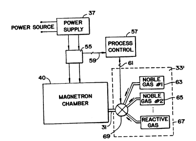
S described with respect to Figure 4. In this example,
particularly for silicon processes, ~ome characteristic
of the power being ~upplied to the magnetron chamber 42
is monitored, rather than the intensity of a plasma
emission line. This is accomplished by introducing a
circuit 55 in the path of the lines from the power
supply 37, or by connection with the power ~upply
directly (not shown). A process controller 57 receives,
over lines 59, a signal representing one or more of the
voltage, current or power being supplied to the
magnetron cathode 17 within the chA~hPr 40. The process
controller 57 controls, through line 61, the relative
proportion of the various gases from a source 33 of
gases that is introduced into the chamber 40. The
purpose of the control system is to maintain operation
with a minimum system impedance. By monitoring power
supply voltage, for example, as shown in Figure 6, the
relative percentages of reactive and noble gases are
controlled in this manner, in order to maintain
operation in the desired stable operating zone. One
advantage of the present invention is that, by allowing
the use of noble gases in reactive sputtering of
silicon, the process can be automatically maintained in
the desired operating zone. This cannot ~ccur when the
atmosphere within the chamber includes only a reactive
gas ~uch as oxygen.
The present invention provides a greater
improvement when the power supply 37 is of a direct
current (d.c.) type, since the arcing problems are most
severe, but also provides improved operation when the
power supply 37 provides alternating current (a.c.) to
the magnetron 40.
215~146
The ~upply 33' of gases introduced into the
magnetron chamber 40 includes a ~upply 63 of a fir~t
noble gas, a gupply 65 of the ~econd noble gas, ~nd a
~upply 67 of reactive gas. Other reactive and/or noble
gases can be employed ~nd introduced into the magnetron
chamber 40 ~t the 6ame time. A valve and flow meter
~ystem 69 both measures the flow of the individual gases
from the various supplies into the chamber ~nd provides
for valve control of those flows. The process
controller 57 receives, over lines 61, information of
the individual gas flows and provides, over the same
line 61, control signals to operate the individual gas
supply valves. In the example of depositing cilicon
dioxide film, the reactive gas ~ource 67 includes
oxygen, one of the noble gas sources 63 or 65 contains
argon, and the other of the sources 63 or 65 contains
- either helium, neon or both. Alternatively, another
source of noble gas can be included so that both helium
- and neon are combined with the argon for use within the
magnetron chamber 40.
The effect of different combinations of noble
gases and a procedure for determining the relative
proportions of each of two different noble gases to be
used, will be explained with respect to the curves of
Figure 5. Curves 71 and 73 ~how the effect on power
~upply voltage, when the total power from the power
supply is maintain constant, as the relative proportions
of two different inert gases are varied. These curves
approximate what occur~ with a silicon target and no
reactive gas, where the noble gas ~1 i6 either helium or
neon and noble gas ~2 is argon. The interesting effect
illustrated in Figure 5 is that the voltage varies
considerably ~s a function the relative proportions of
noble gases #1 and ~2, particularly at high power which
is usually desired in order to obtain a high deposition
rate. An optimum operating point, from a theoretical
point of view, is that a relative mixture indicated at
75, when operating ~t the low power of the curve 73, or
at 77, when operating on the higher power curve 71. It
is the reduced power 6upply voltage that minimizes the
probability of ~rcs occurring while, at the ~ame time,
resulting in a maximum current for the given constant
power. The ~ystem follows a fundamental electrical
relationship of the total power supplied to the
magnetron being equal to the voltage:applied across the
target and anode, multiplied by the current ~o ~upplied
(p = V x I).
Since these exact minima of the curves 71 and
75 may not be easily maintained in co~mercial sputtering
applications, operation is maintained within a range of
lS different proportions of noble gases #1 and ~2. In the
case of films of silicon or silicon compounds, the noble
gas with the lowest atomic number will generally
constitute the majority. Helium (atomic number of 2)
and neon (atomic number of 10) are both lower in atomic
number than argon (atomic number 18). An operable
range, however, has been found to be broader than that,
namely 20 to 80 percent of the noble gases being argon
and the balance being either neon or helium or a
combination of neon and helium.
Once one or more curves of the type ~shown in
Figure 5 are determined for a particular target material
in a particular magnetron ~puttering ~ystem, a
proportion of two or more different noble gases is
established. It iE then ~nown ~hat the partial
pressures cf each of the noble gases within the
magnetron chamber 40 maintain that given percentage with
respect to the partial pressure of all of the noble
gases within the chamber. These relative partial
pressures are maintained by the process controller 57
(Figure 4) controlling the rates of flow of the two or
more noble gases into the chamber 40 with the determined
.- 2155145
relative proportions. Once determined, those relative
proportions remain fixed while the process controller 57
var~es the relative proportion of ~11 noble gases and
the reactive gases in accordance with the relationship
of Figure 6, in order to maintain operation within the
~table zone. As an alternative to the use of 6eparate
~ources of each of the noble gases, they may be premixed
in a Fingle container that is then used as the ~ole
cource of the noble gases.
It can be seen from the curves of Figure 5
that a combination of two noble gases results in the
ability to operate the magnetron with a voltage that is
significantly less than if only one of the noble gases
is utilized. Indeed, it is advantageous to be able to
reduce that voltage, for a given constant power, ~y as
little as 2 percent. Even such ~ small decline in
voltage decreases the probability of arcs occurring. A
decrease of 10 percent or more in operating voltage
brings about an extremely large improvement in the
sputtering operation.
Although the method of determining a range of
useful mixtures of two different noble gases has been
described with respect to ~igure 5 by holding the power
constant and measuring the vGltage, the ~ame effects can
be obtained by controlling and monitoring other
combinations. For example, rather than measuring
voltage when the power is constant, the current supplied
to the magnetron chamber 40 can be measured. The
current reaches a maximum where the voltage of the
curves of ~igure 5 are a minimum. Operation is then
controlled in order to obtain a higher operating current
than possible with use of only one noble gas.
Similarly, the voltage of the ~ystem can be maintained
constant by the power supply 37 and operation set for a
low power or high current. Lastly, the current to the
magnetron cathode 17 can be maintained constant,
215~146
16
operation being set ~t a reduced voltage or increased
power as A result of mixing two noble gases together.
Although the various ~spects of the present
invention have been described with respect to a
preferred embodiment, it will be understood that the
invention is entitled to protection within the full
scope of the appended claims.