Note: Descriptions are shown in the official language in which they were submitted.
21~33~
.
ELECTRONIC CIRCUIT LMPLEMENTING
COMPONENT LEVEL DISK DRIVE
Field of the Invention
The present invention relates generally to electronic devices ~ m~ntin~
local storage, and in particular to an electronic circuit that incorporates a component
level disk drive in lieu of costlier solid state memory.
Background of the Invention
Solid state memory is a standard component of computer systems and of many
electronic devices, providing local storage to the electronic circuit that incorporates
it. Some examples of solid state memory components are flash EPROM (erasable,
programmable read-only memory), SRAM (static random access memory), and DRAM
(dynamic random access memory). One useful function of local memory is to hold
small amounts of microcode to be used, for example, for programming programmablecircuit components, or for running basic assurance tests (BATS) on other the
circuit components. Another useful function of local memory is to store user
information, e.g. Iocal storage is used by a pager to store telephone numbers and
messages, by a fax machine to store, ( Atinn protocol parameters, by a printer
to store fonts, and so on. For reliability and flexibility, the solid state memory used
in such applications is non-volatile and modifiable, e.g. SRAM.
Unfortunately, the cost of solid state memory increases almost linearly with itsstorage capacity . Moreover, since there are physical limitations to known solid state
tl~nhnnlngi~q~ an increase in the storage capacity of memory corresponds to an
increase in its physical size. These 1 tinnc present a foreseeable problem with
the growing demand for small, sophisticated, portable, and inexpensive devices
with substantial storage ~ uir. ' .
Clne area in which the limitations of solid state memory are becoming apparent
is card-based electronic circuits. For example, circuits embodying or controlling
fax machines, modems, cellular phones, printers, cameras, disk drives, und otherdevices are presently being housed in credit-card sized formats of predefined
~' ~inn~q that plug into a, _ tihl~ socket of a laptop computer, PC, or other
electronic device. Three standard formats that have emerged for such credit-card-
SA9-94-128
21~381
type applications are the PCMCIA formats. A "type III" card measures 10.5 mm in
height, 5.6 mm in length and 54 mm in width. The (~- nn~ of a "type II" card are
~r- trly 3.3 mm high X 85.6 mm long X 54 mm wide. A "type I" card is a
modest 2.5 mm high X 85.6 mm long X 54 mm wide.
In contrast to solid state memories, magnetic disk drives in general are
becoming smaller, and their cost per megabyte is decreasing. It is therefore
advantageous to provide a magnetic disk drive small enough to replace solid state
memory in electronic devices, such as printers, and in card-based electronic
circuits, e.g. PCMCIA formats. Furthermore, magnetic disk drives are ideal for
many of the applications discussed above because they provide modifiable, high
density, nonvolatile storage.
Until recently, however, magnetic storage devices have been to large to
incorporate directly into an application circuit such as those implemented in PCMCIA
type card enclosures. Rather, drives have traditionally been peripheral devices
~ r~ting with the application through a peripheral interface. Moreover,
removable, card-based electronic circuits and many electronic devices in generalmust remain operational after being dropped or otherwise exposed to external shock.
Previous disk drives were unable to withstand large amounts of external shock
without suffering damage, because the shock caused the read/write heads and
suspensions to slam into the magnetic recording surfaces.
Recently, a number of small disk drives have become available on the market
approaching a component-sized storage device . For example, ~ewlett Packard offers
a 20-40 MB 1. 3" KittyHawk~M drive . In addition, rnmrnnent type drives are disclosed
inU.S. PatentNo. 5,264,975, Japaneseapplicationnos. 62-270089, 04-291079, and
Japanese publication no. 01112586. Elowever, none of these references discusses an
architecture for implementing a disk drive as local storage within an electroniccircuit, wherein the circuit performs functions unrelated to the operation of the disk
drive itself, e.g. a circuit wherein the disk drive stores microcode for use in the
operation of the circuit, or wherein messages received by the circuit are stored in
the disk drive.
Summary of the Invention
A primary object of the present invention is to provide an electronic circuit
implementing a discrete, component-type disk drive in lieu of solid state memory for
SA9-94-128 2
21~381
local storage requirements, wLqerein the electronic circuit uses information stored on
the component drive to perform functions unrelated to the operation of the disk
drive.
A further object of the present invention is to provide an electronic circuit in5 a card enclosure, e.g. a PCMCIA type II or III card, and including therein a low
profile component sized drive having a footprint of less than 50% of the card area,
and good resistance to external shock.
Another object of the present invention i8 to provide an electric circuit
implementing a, ~ t disk drive for locally storing basic assurance tests.
A further object of the present invention is to provide an electronic circuit,
including a programmable logic unit (PLU), and implementing a component disk drive
for locally storing the microcode used to program the PLU.
Yet another object of the present invention is to provide an electronic
~ nf device includin~ a component disk drive for storing messages, images,15 documents, videos and other user information.
AccordiLqgly, the present invention is an electronic circuit apparatus
comprising an electronic circuit implementing a discrete, component sized disk drive
in lieu of solid state memory for locally storing information to be used by said circuit
in performing one or more functions not related to the operation of the disk drive.
20 In the preferred embodiment, the disk drive comprises a single disk with a diameter
of no more than 1.3 inches and a single recording surface, mounted directly to arotatable flat motor having a diameter of up to 1.3 inches. The component drive
further comprises a single suspension carrying at least one transducer for writing
and retrieving data from the disk, and a parking zone at the center of the recording
25 surf~ce for high shock resistance.
In a first specific embodiment of the proposed apparatus, an electronic circuit
including a component disk drive is provided wherein the disk drive stores microcode
for use in the operation of the circuit. In another specific embodiment, an electronic
circuit including a component disk drive is provided wherein the disk drive stores
30 user information such as telephone numbers and messages.
Brieî Description of the l~rawing
SA9-9~-128 3
21~381
.
The foregoing and other objects, features and advantages of the present
invention will be apparent from the following detailed description of the preferred
embodiments of the invention, and from the accompanying figures of the drawing:
Fig. 1 is a circuit board including a discrete component sized disk drive for
local storage re~uir~ b according to the present invention;
Figs . 2 (a) and 2 (b ) show a known disk drive including two recording surfacesand two suspensions;
Figs. 3(a) - 3(d) show side and top views of the component disk drive for use
in the preferred embodiment of the present invention;
Fig. 4 is a perspective view of a general card-type electronic circuit
enclosure;
Fig. 5 is a top exposed view of a card enclosure housing an electronic circuit
that includes a component disk drive for local storage l't~lUi~'~ ts according to the
present invention;
Fig. 6 is a functional block diagram illustrating a specific rmho~ t of an
electronic circuit apparatus according to the present invention; and
Figs. 7 and 8 are functional block diagrams illustrating additional specific
embodiments of the circuit apparatus according to the present invention.
Description of the Preferred ~ '
The present invention will now be described with reference to Fig. 1,
illustrating a general electronic circuit board 4 representative of circuit boards
found in a variety of electronic devices. It includes a plurality of interconnected
circuit elements 5 such as solid state ~ A ~nrntc~ resistors, capacitors, oscillators,
and so forth. The solid state rrmrnn~n~s comprise, for example, a microprocessor,
memory, an arithmetic logic unit, a pl"~ hle logic unit, etc. The
interr~nn~rtrd elements are referred to collectively as the electronic circuit. The
electronic circuit also includes a discrete, component-sized disk drive 6 according
to the present invention for providing local storage to one or more of the circuit
elements 5.
A circuit board such as that represented in Fig. 1 may reside, for example,
in a personal computer, a laptop, or other computing device. It may also reside in
devices peripheral to a computing device, e.g. controller cards for larger disk
drives, printers, modems, fax-modems, and servers. A circuit board is often
SA9-94-128 4
21~3381
present in electronic devices such as video cameras, fax machines, cellular phones,
electronic pagers, photocopiers, and remote control devices. All of these are likely
to have electronic circuits with some local storage r~lui~. ts.
Figs. 2(a) and 2(b) show side and top views of a general, presently known
5 disk drive comprising a disk or platter 11 connected to a hub 15, a motor (notshown), an actuator assembly 12, arm electronics 17, and a housing 16. The disk
11 includes a pair of recording surfaces 8,9. The actuator assembly 12 generallycomprises a voice coil motor (VCM), an actuator arm 6, and a pair of suspensions 13
t-nnnf~nted to the arm 6 and supporting a pair of air bearing sliders 14 over
10 r~ e~:~iv~ recording surfaces 8,9 of the disk 11. One or more transducers or
read/write heads are located on each slider 14, and are held in close proximity to the
disk surface by the combination of a downward force (relative to the disk surface)
from the suspension 13 and an upward force caused by air flow generated from therotation of the disk 11. If the downward force exceeds the upward force, the slider
15 will come into contact with the disk surface.
The VCM comprises an inductive coil 19 disposed between an upper magnet
(not shown) and a lower magnetic plate 7 . The arm electronics 17 transmits electrical
positioning current to the coil 19. The current signal induces a magnetic flux
around the coil for repulsing and attracting the magnet and magnetic plate 7. The
20 repulsing and attracting forces provide movement of the actuator arm in a plane
substantially parallel to those of the disk recording surfaces, causing the
suspensions 13 to move along an arcuate path over respective surfaces 8,9.
Data is generally recorded on rnnl~ ~ntri,- tracks of the recording surfaces 8, 9 .
The disk region or track having the largest diameter is referred to as the outer25 diameter (OD) of the disk, and the region or track nearest to the hub and having the
smallest diameter i8 referred to as the inner diameter (ID) . Data to be stored on the
disk 11 is first "encoded" by a read/write channel (not shown) ordinarily residing
external to the disk drive housing 16. The data is encoded into a form suitable for
the storage medium, then transmitted via the arm electronics 17 to the transducer
30 for writing to the disk. For example, in a magnetic disk drive, digital data is
encoded into ~ series of pulses. As is known in the art, the pulses are transmitted
in the form of a current to the transducer, and cause a flllnt~ tin~ magnetic field at
the transducer pole tip that affects the magnetization of discrete regions on the disk
surface. When a transducer senses or "reads" information from the disk, the data
SA9-94-128 5
~ 53~1
is transmitted in encoded form via the arm electronics 17 to the channel ~or
"decoding". The arm electronics usually include means for amplifying and
synohroni~ing the read signal.
The hub 15 is fixedly attached to the disk 11 and encases a motor (not shown)
5 for providing a rotational force. The rotational force is translated to the hub 15 and
from the hub 15 to the disk 11. The hub encloses a motor shaft and generally
protrudes from the upper surface of the disk as shown in Fig. lA, preventing thesuspension/ head assembly from access to the region at the center of the disk. To
protect a rotary disk drive from external forces during operation or movement,
10 means may be implemented to park the head when the disk is not operating and/or
during periods of inacffvity (i . e . times when data is not being written to or retrieved
from the disk).
Figs. 3(a)-3(d) show the preferred: ' -nt of the component disk drive
implemented in the electronic circuit apparatus of thepresent invention. The drive
comprises a disk 11, a motor 44, an actuator assembly 12, arm electronics 17, and a
housing 16. The disk 11 is preferably magnetic and includes one recording surface
42 with a substantially planar region 45 at its center. It is preferably mounteddirectly to a flat motor 44 along its nonrecording surface by some appropriate means,
e.g. mechanically, or by applying a bonding agent along interface 43. Use of a
single recording surface and direct platter mounting allows a wider, thinner motor
assembly to be used than would be feasible for a disk having two reoording surfaces .
The diameter of the motor 44 may be as large or larger than the diameter of the disk
11 itself. The advantages of this type of motor 44 will be described in further detail
below .
Theactuatorassemblycomprisesavoicecoilmotor, anactuatorarm6, asingle
suspension 13 and a transducer-bearing slider 14. Preferably, the slider carries a
magnetoresistive (MR) head for greater data capacity. Magn~ur~bib~iv~ heads are
known in the disk drive industry and are preferred because their high sensitivity
enables greater areal density (i . e . bits per inch) than conventional inductive heads .
3 0 Using a state of the art magnetoresisffve head in the preferred embodiment provides
useful data storage capacity for applicaffons requiring moderate data storage.
However, it will be understood that other types of transducers may also be
implemented. Moreover, the invention may easily be adapted for a plurality of heads
per slider and a plurality of sliders on Cllqpf~n~irm 13.
SA9-94-128 6
21~a381
Direct mounting of disk 11 to motor g4 creates an unobstructed region 45 at the
disk's center 41 accessible to the actuator assembly 12. The diameter of recording
tracks in this region would be too small for practical use, so the region is used for
center parking. Figs . 3(a) and 3(b) show head 14 and suspension 13 positioned over
the data recording surface of disk 11. During times of inactivity, the head is
"parked" in the central region 45 as shown in Figs. 3(c) and 3(d) so that head 14 is
substantially aligned with a central access 41 perpPn~ r to the disk surface. Asthe slider 14 nears the inner diameter of the disk 11, the upward force of the air flow
is reduced and the slider begins to drag along region 45. It is then "parked" at the
disk center 41 as shown. Parking structures, e.g. ramps, may be added to the
center parking region to facilitate parking. Spacer structures may also be provided
between this region and the upper drive housing for added structural support.
The actuator assembly 12 moves the slider back onto the disk surface when
necessary by applying a force to overcome the stiction between slider 14 and surface
8. "Stiction" is a term of art for the attractive and frictional forces between slider
14 and surface 8. It is greatest at the outer diameter of the disk and decreases in
the direction of the disk center, being essentially reduced to zero at dead center.
Since the slider is parked at disk center 41, stiction is virtually nonexistent, and
very little force is required to overcome it.
2 0 The slider 14 is preferably also center parked during periods when the drive
is not operational. When the drive is powered on, the disk 11 spins without any
nifi~nt stiction imrP-~n( ~ Reduced stiction translates to a reduction in
starting torque required from the motor 44. Reduced starting torque in turn leads
to a reduction in the electric power requirements of the drive.
As mentioned previously, the preferred embodiment of the component disk
drive allows a flatter, wider motor 44 to be used than conventional disk drives
requiring hubs. The motor may take a variety of forms. For example, it may be
ffxed to the disk drive housing or integrated therein. It may have the shape of a
disk, or be annular in shape. It may include a hub, and the disk may be mounted
directly to the hub, or alternatively, the hub may penetrate the disk and lie
substantially flush with the recording surface to preserve actuator access for center
parking. An annular motor may surround a stationary hub structure that lies flush
with the recording surface to provide a stationary parking ~one at disk center.
SA9-~34-128 7
21~381
Those skilled in the art of motor design generally understand that an increase
in the diameter of the motor windings increases its moment arm to generate more
torque with less force. The motor thus requires less electric current to perform the
6ame operation as a center hub motor. Since the electrical power ~P) is proportional
5 to the square of the current, a reduction in the current ~ uir,~ lt will result in
a large reduction in the electric power r~lui~. ' as shown below.
(1) P = I x I x R, and
(2) I = k/D.
Therefore,
(3) P = (k x k x R)/ (D x D),
where P is the electric power of the motor, I is the electric current used by the
motor, D is the motor diameter, R is the electric resistance of the motor, and k is the
inversely proportional constant of the motor current to diameter. Applying the
above equations, an increase of motor diameter by, for example, a factor of 3 will
result in a motor that can achieve the same torque with 1/9th of the power. The
motor torque is transmitted directly to the bottom surface of the disk through, for
example, an adhesive or a coupling device. Examples of motors that may be used to
implement the preferred embodiment include those implemented in the ui,~lly
available IBM TravelstarTM, and the Maxtor MobileMax Lite~M.
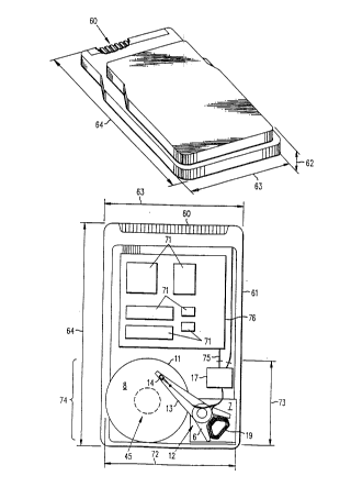
Fig. 4 is representative of a card enclosure for an electronic circuit, adapted
to be plugged into a compatible computer slot at connector 64. It may, for example,
be a PCMCIA card type I, II or III having a predefined length 64, width 63, and
helght 62. The card thickness 62 is generally the most critical, ~ n of a card
enclosure .
Fig. 5 illustrates generally the preferred embodiment of the electronic circuit
apparatus of the present invention. The circuit implements a discrete, componentsized disk drive 74 for local storage and resi~es in a card enclosure such as a
PCMCIA type II or type III format, although it will be understood that the circuit
apparatus of the present invention may also be enclosed in other card formats, or
may comprise the electronic circuit of an electronic device and reside within the
SA9-94-128 8
~ 2i~5381
device enclosure rather than within a card enclosure (e.g. a camera). The disk
drive assembly 74 preferably measures no more than 2 inches in length 72 X 1.6
inches in width 73 X 5 mm in height.
For example, a 1.3" magnetic disk is mounted to a small, flat motor such as
5 that implemented in Maxtor's MobileMax Lite. (At present there are no flat motors
under 5 mm, ~ially available for implementation in a type II design. However,
availability is aneicipated in the near future and prototypes are currently being
tested. ) The actuator assembly is a conventional dual-suspension design such asthat used in the Hewlett Packard KittyHawk 1.3" drive, modified to have a single10 suspension with a magnetoresistive head. Modifications required for operability
include removal of the lower suspension and any actuator arm height adjustments
necessitated by the height of the direct-mounted disk. It may also be desirable to
make A~litil~nAl ~ifi~ Ati~n~ e.g. reducing t~le height of the actuator assembly.
The manner of making such m~llifi(~Ati~ln~ will be readily apparent to a person of
15 ordinary skill in the operation of disk drive assemblies in view of this 5pPrifi~Ati--n
and the state of the art.
The disk drive assembly 74 preferably occupies less than 50% of the available
card area and has an orientation such as that shown. Alternatively, the drive isoriented such that its lengtll 72 is parallel to the length 64 of the card. The
2 0 remaining card area is populated by a plurality of electronic components 71
comprising an application subcircuit.
The control functions required to control operation of the drive preferably
reside on one or more of the integrated circuit (IC) components 71 within the card
enclosure. As those skilled in the art will appreciate, the control electronics include
25 functions such as servo control, an interface, data, address and command buffers,
drive motor controls, and a read/write channel. Since the component disk drive is
small, the control electronics will be in close proximity to the drive itself. It may
therefore also be desirable to include the arm electronics 17 within the controlelectronics rather than within the disk drive enclosure. The circuit components
30 embodying the control electronics may be dedicated to storage control, or mayadditionally include non-storage functions . For circuits housed in non-PCMCIA card
formats, it may be desirable to locate the storage control components external to the
card, e.g. within the electronic device into which the card is plugged.
SA9-94-128 9
21~381
Referring back to Fig. 5, subcircuit components 71 are mounted to an
electronic circuit board 76 occupying the portion of the card unoccupied by the
device assembly 74. Conductive means 75, e.g. a flex cable or other connector,
couples the drive assembly to the circuit components 71. The conductive means 75include, for example, control lines, a data bus, and an address bus. If the
components controlling the operation of the drive are external to the card enclosure,
the app~opriate control lines are routed to connector 60 to provide external access
to the assembly 74, as shown.
The drive assembly 74 is preferably enclosed in a separate housing (not
shown) within the card enclosure isolating it from the other components for
protection against contaminants. Alternatively, the card may be subdivided into two
or more isolated sections, or card producffon may be carefully controlled to minimize
the presence of contaminants in the enffre card.
Numerous types of electronic devices currently include electronic circuits that
use solid state memory for local storage re(lui~. tc. A11 of these are viable
~n~litls~ti~: for implementing a component disk drive in lieu of memory according to
theelectroniccircuitapparatusofthepresentinvention, including, forexample, fax
machines, cellular phones, printers, cameras, appliances, and portable computingdevices .
Fig. 6 is a funcffonal diagram of an electronic circuit apparatus according to
the present invention wherein the component disk drive 74 is used for storing
microcode. The circuit includes a p~-U~;I. hlf~ logic unit (PLU) 127 for performing
one or more desired functions which are defined by one or more microcode sets . The
PLU may, for example, be programmable array logic (PAL), a programmable logic
device (PLD), oramicroprocessorwith~ro~. hlf~functions Eachmicrocodeset
corresponds to a unique PLU funcffon. The PLU 127 typically is linked to one or
more non storage related cirouit . r.mrnn~nt~ 128 and may function, for example, as
a disk interface between the components 128 and the disk drive 74, as a
microprocessor, or as an aritl~metic device. The microcode sets are stored locally,
i.e. in the component disk drive 74, and then pro~, into the unit 127 via a
logic programmer 125. Since information on a disk drive is easily updated,
additions, deletions, and other mo~lifi~ ~tif~nq may readily be made to the microcode
sets .
SA9-94-128 10
21~381
The component drive ~4 is linked to drive control electronics 123. In the
interest of conserving space, the drive control electronics are merged with logic
pru~l 125 into a controller device 122 such as a solid state component, die,
multi-chip module, or electronic assembly. The controller 122 optionally includes
other functions 124 unrelated to drive control and PLU programming that may require
further links to one or more Ar1~1itinn~1 circuit components 126.
Fig. 7 shows another specific embodiment of the present invention, wherein
the component disk drive 74 stores basic assurance test (BAT) code and tables. As
described earlier, BAT code typically resides in~EPROM or flas~l memory, and runs
diagnostic tests against components of the circuit to verify their operability.
Verification testing is a desirable feature for card-based applications and electronic
devices in general to assure their reliability.
Referring to Fig. 7~ a component disk drive 74 and its ~ o~ tPd drive
electronics 123 are linked to a microprocessor 91 which initiates execution of the
BATs. The microprocessor is linked to high speed static ram (SRAM) 92, which, inturn, is linked to test circuitry 95. The test circuitry is part of a circuit loop
including the circuit ~ ~nPnt~ 104-106 to be tested.
When the processor 91 is in test mode, it receives test microcode from
t drive 74, including a table of test patterns that are loaded into SRAM 92 .
The table includes a plurality of binary input test patterns 93 and their
~uLL~ullding results 94 expected from a properly working circuit. The next test
pattern to be executed and its corresponding expected result are provided to thetest circuit, e . g. by loading tllem into input buffers 96, 99 . The test pattern is then
forwarded to the components under test, e.g. via an output buffer 98, unless an
error signal has been detected by control means 97. Buffers 96 and 98 may actually
comprise a serles of n latches, where n is the number of bits in the test pattern, and
the control means 97 may comprise an inverted error signal coupled to the clock
inputs of these latches.
Assuming no error, the next sequential test pattern is loaded into input buffer
96 and the current test pattern is passed through the circuit components 104-106.
Each component under test receives the pattern and performs its particular function
upon it. The final result is then returned to the test circuitry 95, e.g. into input
buffer 102. Comparing means 101 such as a comparator then compare the result in
buffer 102 with the expected result in buffer 99. If a mismatch occurs, an error
SA9-94-128 11
2~5'381
signal is generated and propagated to control means 97 to halt execution of the next
pattern in the test sequence. It is also provided to error handling functions (not
shown~, such as retry circuitry, error indicator means or shutdown means. If a
mismatch l~as not occurred, the next test pattern is passed to the circuit components
and the preceding steps are repeated until an error is detected or the test sequence
is completed. The functions of test circuit 95 may alternatively be performed by a
computer program stored in the component drive 74 and executed by the processor
91 .
Another use for a component disk drive is for storing user information. A
component drive may be used, for instance, to store telephone numbers, messages,and similar information in any type of portable wireless ~ ~ lg device.
State-of-the art portable message devices that rely cn solid state memories are
limited in the amount of information they can store, making them impractical forreceiving large documents, electronic mail, pictures and video images. This
limitation is overcome by replacing the memcry with a component disk drive.
Fig. 8 shows a functional diagram of an electronic circuit apparatus 131
according to the present invention thAt operates as an electronic pager, wherein a
_ ~nPnt disk drive 74 provides resident storage for telephone numbers, messages,and other user information . The device is packaged as a peripheral device, e . g. in
a PCMCIA card format, or in an independent device packaged conveniently for
handheld manipulation.
The pager apparatus 131 of Fig. 8 includes an electronic circuit typical of a
conventional digital pager. A ~ rrb~rJr 132 cQntrols the operation of the device.
The processor 132 is coupled to a frequency monitoring wireless receiver circuit 141
comprising, for example, an antenna 134 and receiver electronics 133. The circuit
also includes some type of readout display 138, e.g. an LCD display. If the pager
is packaged as a peripheral device, it further comprises means for ~ , Atin~
with a computing device 139, e.g. PCMCIA interface electronics 136 disposed
between the processor 132 and the card connector 137.
In operation, the wireless receiver circuit 141 "listens" on a predetermined
frequency for a particular code or signal inrli~Atin~ a message is to be transmitted.
In listening mode, the r~r mrnnPnt drive 74 is powered down to conserve energy.
Upon detecting the proper code, the receiver electronics 133 signals the processor
132 to power up to the component drive 74. The receiver circuit 141 then receives
SA9-94-128 12
21~381
the message in the form of eltt~:Lrl ~ -tic radiation and converts it to digital electric
impulses. These, in turn, are transmitted via the processor 132 to the drive
electronics 123 and are stored ~nPti~lly on the component drive 74. Once the
message is received, the display 138 may display the message or post a notice that
5 a message has been received. Then the drive 74 is again powered down, and the
circuit returns to a listening mode.
The pager circuit just described is capable of storing lengthy messages. For
independent devices, this would nP~`PCCit~tPC a reasonably large display means.
Alternatively, if the device is implemented as a peripheral, messages can be stored
lO away for later access. The user then displays his messages by plugging the device
131 into a computing device 139, e.g. a laptop computer. The computing device
accesses the information on the component drive 74 and displays it on a monitor (not
shown) .
Since the, t drive of the pager implementation of Fig. 8 is powered
15 down much of the time, energy consumption of the unit is relatively low.
Consequently, the circuit may be powered by an in~t~pPn~TPnt power source, such
as a battery pack 135. Alternatively, or in addition, it may rely on a power supply
(not shown) in computing device 139.
A peripheral pager can be carried much like a digital pager, using it's
20 batteries to power up the component drive when necessary. Since messages are
- ~ist1-Ply received and available for access, the user is no longer required to place
a phone call to obtain the information. Standard encryption techniques are
preferably employed for security to assure the security of the information. In
addition, the device preferably further comprises a wireless transmitter (not shown)
25 for return communication. Information to be transmitted is entered into the
computing device 139 and downloaded into the component drive. It may then be
transmitted 'izttPly, or at a later time.
SA9-94-128 13
2i~381
Although the electronic circuit apparatuR of the present invention has been
described in terms of specific embodiments, it is to be understood that this
disclosure is not to be interpreted as limited to those embodiments shown. Various
further alterations and moflifieRti~-nR will no doubt become apparent to those skilled
5 in the art after having read the above disclosure. Moreover, the examples provided
are not intended to be exhaustive, and the scope of the present invention defined
by the following claims is intended to extend to all functional equivalents of the
elements shown or described.
SA9-94-12~ 14