Note: Descriptions are shown in the official language in which they were submitted.
WO94/19676 2 ~ 2 PCT~S94/01204
SOLID STATE SPECTROFLUORIMETER
~ND M~THOD OF USING THE S~ME
BACKGROUND OF THE lNV N'~:lON
1. The Field of the Art.
The present invention relates to a
spectrofluorimeter.
2. Description of the Related Art.
Spectrofluorimeters are used to detect the
presence of certain molecular structures in a
specimen. Specifically, in the presence of a
solution cont~;n;ng a fluorophore, certain molecular
structures are known to interact with the
fluorophore such that the incident light of a
particular wavelength is absorbed ancl light having a
different wavelength is emitted. Measuring the
light emitted at the fluorophore wavelength, due to
the presenc~ of the molecular struct-lre of interest
in the specimen, allows for the determination of the
quantity of the mol~c~llAr structure of interest in
the specimen.
For example, ethidium bromi.de (EtBr) is
used a fluorophore to detect the presence of nucleic
acids by virtue of its intercalation into the
nucleic acid chain. Monochromatic li.ght having a
wavelength of 520 nanometers is irracliated on the
solution containing the specimen of i.nterest. By
measuring the quantity of light emitt:ed at a
wavelength of 600 nanometers allows t:he
concentration of the nucleic acid in the specimen to
be determined.
WO94/19676 ~ PCT~S94/01204
2~
While spectrofluorimetry has been known
many years, spectrofluorimeters are typically very
largè in size, delicate and exceptionally expensive.
Many reasons for this exist.
One such reason is that
spectrofluorimeters typically require a very large,
steady state light source. Such a light source
generates large quantities of heat, which requires
the distance of the light source from the specimen
to be quite large. Furthermore, these light sources
typically require mech~n;cal choppers and
complicated light directing mech~isms. For
example, reference is made to U.S. Patent Nos.
3,832,555 and 4,531,834.
Furthermore, in order to have wide
commercial applications, the detectors of the
spectrofluorimeter must be adaptable for use with
widely available fluorophore dyes. Furthermore,
electrical noise generated by the light source is
high in spectroflourimeters generally. These
factors have inhibited the use of solid state
detectors being used in spectrflourimeters. In the
past, Hofer Scientific offered a solid state
detector spectroflourimeter, but this
spectroflorimeter could only measure Hoechst dyes
due to the requirement that it detect in infrared
wavelengths. Thus, this spectroflourimeter could
not be used to detect wavelengths in the visible
spectrum. Also, the specimen itself was destroyed
when using the Hoechst dyes.
WO94119676 PCT~S94/0~04
SUMMARY OF THE lN v~llON
It is an object of the pre~sent invention
to providé a solid state spectrofluorimeter having
high immunity from undesired noise.
It is another object of the present
invention to provide a solid state
spectrofluorimeter that uses a triggered light
source.
Another object of the spec1:rofluorimeter
according to the present invention is to provide a
solid state spectrofluorimeter that requires a low
power light source.
It is a further object of t:he present
invention to provide a solid state
spectrofluorimeter capable of detecting light in the
visible spectrum using commercially a~vailable
fluorophores.
Still a further object of the present
invention to provide a spectrofluorimeter of compact
size and which is easy to use.
In order to attain the above recited
objects of the invention, among others, the present
invention advantageously uses a triggered xenon
flash tube. Powered with a capacitor store, the
xenon flash tube is connected in parallel with a
matched resistive load, which resistive load
increases the lifespan of the xenon flash tube as
well as increases the duration of the light pulse
itself.
Furthermore, spectrofluorimeter according
to the present invention uses an optical cell having
a configuration in which the xenon flash tube is
placed in spaced relation to a pair of signal
WO94/19676 ~ PCT~S94/0~04
S~
detectors and a reference detector. The spaced
relation of these components substantially helps
allow the use of solid state detectors in the
spectroflourimeter. t
The spectroflourimeter according to the
present invention also provides electrical isolation
of the detector amplifiers during all periods except
for the actual detection portion flash cycle. This
helps enhance the noise immunity of the
spectroflourimeter detection system.
Also, the solid state spectrofluorimeter
according to the present invention advantageously
uses a microcontroller to ~o.lLLol the flash timing
of the Yeno~ flash tube and the timing of electrical
isolation of the detector amplifier circuits.
Thus, the solid state spectrofluorimeter
described above advantageously allows the detection
of molec~ r structures in a specimen using a
commonly available fluorophores detectable in the
visible spectrum.
BRIEF DESCRIPTION OF THE DRAWINGS
These and other advantages of the present
invention may be appreciated from studying the
following detailed description of the preferred
embodiment together with the drawings in which:
FIGURE 1 illustrates a block diagram of
the spectrofluorimeter according to the present
invention;
FIGURE 2 illustrates a perspective view of
the optical cell according to the present invention;
FIGURE 3 illustrates a left side view of
the optical cell according to the present invention;
PCT~S94/0~04
WO94/19676
2 2
FIGURE 4 illustrates a ricJht side view of
the optical cell according to the present invention;
FIGURE 5 illustrates a cross section view
taken along line A-A the optical cell illustrated in
figure 3;
FIGURE 5A illustrates a cross section for
another embodiment of a portion of the optical cell
illustrated in Figure 5;
FIGURE 6 illustrates a crass section view
taken along line B-B of the cell illustrated in
figure 3;
FIGURE 7 illustrates a cross section view
taken along line C-C of the cell illustrated in
figure 3;
FIGURE 8 illustrates a cross section view
taken along line D-D of the cell illustrated in
figure 3;
FIGURE 9 illustrates the initial
amplification circuitry used with the left signal
detector of the spectrofluorimeter according to the
present invention;
FIGURE lO illustrates the :initial
amplification circuitry used with the~ right signal
detector of the spectrofluorimeter ac:cording to the
present invention;
FIGURE 11 illustrates the i.nitial
amplification circuitry used with the reference
signal detector of the spectrofluorimeter according
to the present invention;
FIGURE 12 illustrates the signal
conditioning circuitry of the spectrcfluorimeter
according to the present invention;
WO94/19676 PCT~S94/01204
ll~S~2~ --
FIGURE 13 illustrates the power supply
circuitry used in the spectrofluorimeter according
to the present invention;
FIGURE 14 illustrates the interface
circuitry used by the spectrofluorimeter according
to the present invention;
FIGURE 15 illustrates the microcontroller
circuitry used with the spectrofluorimeter according
to the present invention;
FIGURE 16 provides a flow chart outlining
the operation of the spectrofluorimeter, controlled
with the microcontroller, according to the present
invention;
FIGURE 17 illustrates various display
options available to the user using the
spectrofluorimeter according to the present
invention; and
FIGURE 18 illustrates samples taken during
a single flash cycle when using the
spectrofluorimeter according to the present
invention.
DET~TT~n DESCRIPTION OF THE PREFERRED EMBODIMENT
Figure 1 illustrates a block diagram of
the spectrofluorimeter lO according to the present
invention. Major components of the
spectrofluorimeter 10 include the optical cell 12,
which includes a xenon flash 14, a left signal
detector circuit 16, a left signal detector 17, a
right signal detector circuit 18, a right signal
detector 19, a reference detector circuit 20 and a
reference signal detector 21. The xenon flash tube
is powered by charge stored in a storage capacitor
WO94/19676 PCT~S94/01204
2 2
located in the power supply circuit 22, which
circuit also supplies power to operate a cooling fan
24.
Signal conditioning circuit 26 received
the detected signals from the left signal detector
circuit 16, the right signal detector circuit 18,
and the reference detector circuit 20. Signal
conditioning circuit 26 amplifies shapes and sums
the detected signals, as well as detected reference
signals, and transmits the same to the
microcontroller circuit 28. Interface circuit 30
transmits signals between power suppLy circuit 22
and microcontroller circuit 28 and signal
conditioning circuit 26 as described hereinafter.
The analysis results obtained from
operation of the spectrofluorimeter L0 are displayed
on display 32, which can be an LED display of
numerical values or a monitor which provides a
graphical display. Keyboard 34 allows entry of the
mode of operation, initial conditions, and various
sensitivity characteristics described hereinafter.
Either discreet function keys or mul1:i-function
up/down keys which allow various entries using the
same up/down key pressed repeatedly and are software
~O~L ammed can be used.
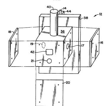
Figure 2 illustrates optical cell 12. The
optical cell 12 contains a machine tooled cell
cavity 36 which is preferably made oi a black
phenolic resin or a flat black anodized aluminum.
Cell cavity 36 is approximately 4 cm3 in outer
dimensions and is mounted on an anod.Lzed black
aluminum plate 38 which shields the xenon flash tube
from the cell cavity 36 except as described
WO94/19676 PCT~S94/01204
5~
hereinafter. Cell cavity 36 is also provided with
an ope~; n~ that allows the insertion of a cuvette
40, which will contain the specimen of interest in
the fluorophore solution. Cell cavity 36 also
contains openings for the left signal detector 17,
the right signal detector 19, reference signal
detector 21 and light absorbing medium 42.
Flash holder 44 supports xenon flash 14 in
place and is made of Corian, an acrylic/aluminum
hydroxide compound. Each of the detectors 17, 19
and 21 disposed in the optical cell 12 are
electrically connected to the left signal detector
circuit 16, the right signal detector circuit 18,
and the reference detector circuit 20, respectively.
Each of detector circuits 16, 18 and 20 are mounted
directly over the detectors disposed in the optical
cell 12. This placement minimizes the electrical
path length the detected signals must travel before
initial amplification, as described hereinafter.
Figures 3-8 illustrate the various cross
sectional views of the optical cell 12. As seen in
Figure 3, the dashed lines illustrate openings
formed in the optical cell 12 for insertion of the
detectors 17, 19 and 21, as well as the cuvette 40.
Furthermore, light pathways are provided by these
openings for the required optical trans~ission
paths.
As seen more clearly in figure 5, which is
the A-A cross section of figure 3, the opening
between the xenon flash 14 and the cuvette 40 is a
rectangular slit 46 having a width of 3mm and a
height of 7mm.
-
PCT~S94101204
wo 94,l9676 2 ~
An alternative to rectangular slit 46 is a
plurality of approximately ten holes 47 having a
diameter of about 0.7mm arranged in a pattern as a
rectangular slit 46, as illustrated in Figure 5A.
Though more difficult to machine such a pattern of
holes 47, this pattern can better focus the light
radiating from the xenon flash 14 to the specimen
within cuvette 40.
The distance between the xenon flash 14
and the cuvette is lOmm. Provided in the optical
pathway is interference filter 54, d.isposed between
the xenon flash 14 and the cuvetté 4l~.
An opening 48 is provided l:o allow the
direct transmission of light generated from the
xenon flash 14 to the reference detec:tor 21.
Or~ g 48 has a diameter of 0.35mm and for
approximately three quarters of the ~5mm distance
between the xenon flash 14 and the reference
detector 20 maintains this diameter. The small
diameter of opening 48 relative to opening 46 helps
dimini~ the amount of light transmitted from xenon
flash 14 onto detector 21. This helps equalize the
amount of light which actually reache;s each of the
detectors 17, 19 and 21.
Figure 6 illustrates more c:Learly the
light absorbing medium 42 disposed directly ~h i nA
the cuvette 40. This helps ensure that light from
the xenon flash tube that passes through cuvette 40
is not reflected and, subsequently, detected by
30,~ detectors 17 and 19. This helps ensur-e that only
florescent light is detected by detect.ors 17 and 19.
Figure 6 also illustrates the larger d.iameter of
opening 48 in the vicinity of reference detector 21,
PCT~S94/01204
WO94/19676
~i5~
which is needed in order to properly position the
reference detector 21. Figure 6 also illustrates
that`neutral density reference filter 52 is placed
between xenon flash 14 and detector 21, directly in
front of detector 21. This further helps equalize
the amount of light which actually reaches each of
the detectors 17, 19 and 21.
Figures 7 and 8 are helpful in describing
the optical characteristics of the optical cell 12.
Referring to Figure 7, it can be seen that the
cuvette 40, which contains the specimen to be
analyzed in solution, and is disposed midway between
each of detectors 17 and 19. Cuvette 40 preferably
has an outer diameter of about 10mm, al~hough a
different size or shaped cuvette 40 can, of course,
be uæed. The preferred distance between the out
diameter of the ~veLLe 40 and each of detector 17
and 19 is 10mm.
Disposed in front of each of detectors 17
and 19 are high h~ndr~Rc emission filters 56 and 58.
These filters eliminate wavelengths below the
wavelength of interest. If ethidium bromide (EtBr)
is used as the fluorophore, each filter 56 is
preferably an OR570 filter that allows light over
590nm to pass while blocki ng virtually all light
having a wavelength below 550nm. Each of high
h~n~r~RR emission filters 56 and 58 are held in
light tight configuration by O-rings 60 and 62.
Each pair of O-rings 60 and 62 are compressed upon
insertion of the detectors 17 and 19 into the
optical cell 12.
Figure 8 illustrates the path 64 that
light from the xenon flash 14 travels to properly
~ ~ ~ PCT~S94/0
WO94/19676
11
strike the specimen solution contained in cuvette
40. Paths 66 and 68 illustrate the path of the
flor~escent light detected by detectors 17 and 19;
respectively, which paths are preferably at 90 to
path 64.
Figure 9 illustrates the left signal
detector circuit 16 represented in block diagram
form in Figure 1 and as a circuit bc~ard in Figure 2.
The detector 17 is preferably a Siem,en's BPX 61
photodiode and, because it is an extremely sensitive
photodiode, is used with no bias voltage.
Operational amplifier 80 provides initial
amplification of the signal detected by detector 17.
The various capacitors and resistors illustrated in
Figure 9 provide proper biasing and wave shaping.
Figure 10 illustrates the right signal
detector circuit which is identical l:o a left sensor
board 16 previously described with referenced to
figure 9. Detector 18 is again a Siemen's BPX 61
photodiode and is also used with no bias voltage.
Care should be taken to obtain detect:ors 17 and 19
that have matched eiectrical characteristics.
Figure 11 illustrates the reference
detector circuit 20 which also uses a Siemen's BPX
61 photodiode as detector 21 and which is also used
with no bias voltage. The detected signal is
amplified by operational amplifier 84. The wave
shaping and noise reducing circuitry associated with
operational amplifier 84 is identical to circuitry
used with the detectors 17 and 19 in order to obtain
maximum performance.
Figure 11 also illustrates that the once
amplified detected signals from detecl:ors 17 and 19,
WO94/19676 PCT~S94/01204
p~5S52~ --
12
respectively, as well as the once amplified signal
from detector 21 are all ouL~uL to the signal
conditioning circuit 26, illustrated in figure 12.
Each of the detected signals pass through
triggered switch 86 during a period of time
determined by the DISABLE signal, described
hereinafter. The detected and once amplified
signals from the left signal detector 16 and the
right signal detector 18 are summed at node 88 and
then twice amplified by operational amplifiers 90
and 92. Again, the associated resistors and
capacitors help with establishing noise immunity and
proper waveshaping.
The reference detector signal is likewise
twice amplified by operational amplifiers 94 and 96.
Identical noise reducing and wave shaping circuitry
is associated with operational amplifiers 94 and 96.
The detected signal 100 o~L~L from operational
amplifier 92 and the reference signal 102 ouL~uL
from the operational amplifier 96 are each input to
the microcontroller circuit 28 illustrated in figure
15 as described hereinafter.
Figure 13 illustrates the power supply 22
used to power the xenon flash 14 and the cooling fan
24 illustrated in figure 1. Power supply 22 powers
the xenon flash 14 using charge stored in capacitor
104. Resistor 106 is used to extend the duration of
the xenon flash tube pulse and also extends the
lifetime of the xenon flash tube by reducing the
voltage across the terminals of the xenon flash
itself. In operation, capacitor 104 is triggered
at 240 volts due to the presence of resistor 106 and
W094/19676 ~ PCT~S94/01204
13
a 600nm pulse of 30,000 watts is obtained, when
integrated over the duration of the pulse.
` The ~A~ signal, input to the capacitor
charging circuit 108, initiates charging of
capacitor 104. Of note, a matched -et of zener
diodes having a 15 volt nominal zener voltage are
used to stabilize the charging of the capacitor 104.
Capacitor 104, when fully charged,
develops a VCAP signal on line 110, which signal is
then input into microcontroller circ:uit 28 and used
as hereinafter described.
When capacitor 104 is ful]y charged, the
xenon flash 14 is ready for firing. Upon receipt
transmission of a FIRE signal along line 112,
silicon controlled rectifier 114 begins conducting.
This causes transmitter transformer 116 to turn on
the xenon flash 14. Thus, charge stored in
capacitor 104 powers the xenon flash 14, which
thereby illuminates the specimen solution in ~e~Le
40 and the reference detector 21, illustrated in
Figure 2.
Also illustrated in figure 13 is an
overvoltage protection device, specifically varistor
118, which will eliminate surges in the voltage used
to charge the capacitor 104.
Power supply circuit 22 ob1tains it DC
power using a stepped power supply configuration.
AC power input from line 120 develops a positive 24
DC volts at node 122 and a negative ;24 DC volts at
node 124 using diodes and smoothing capacitors. A
positive 12 DC volts is obtained using a three
terminal positive voltage regulator 26 such that a
positive 12 DC volts result on line 128. This
c
WO94119676 PCT~S94/01204
~ 14
positive 12 DC volts is then input into two
different three terminal low current 5 volt positive
DC règulators 130 and 132 to obtain VCC DC voltage
and positive 5 DC volts. Similarly, the negative 24
volts from line 124 is input into a three terminal
low current 5 volt negative DC regulator 134 in
order to obtain negative 5 DC volts.
Figure 14 illustrates the interface
circuit 30 between the power supply circuit 22
illustrated in Figure 13 and microcontroller circuit
28 illustrated in Figure 15. VCAP and the AC signal
are pAS~ directly from the power supply circuit 22
to the microcontroller circuit 28. However, the
FIRE signal received from microcontroller circuit 28
is first amplified using up amp 140. The FIRE
signal is then supplied to the power supply circuit
22 to fire the xenon flash 14 as described
previously. The CHARGE signal is input from the
microcontroller circuit 28 to a flipflop 142.
Flipflop 142 maintains at its output a signal
corresponding in level according to the CHARGE
signal until microcontroller circuit 28 develops
another r~ signal in response to an input of the
VCAP signal previously described. This ensure that
capacitor 104 of Figure 113 is fully charged prior
to firing of xenon flash 14.
As also illustrated in figure 14, the FIRE
signal, as amplified by operational amplifier 140,
is then also used as the DISABLE signal input to
signal conditioning circuit 26. The DISABLE signal,
as described previously, effectively connects the
detectors 17, 19 and 21 to the signal conditioning
circuit 26, as switches 86 of Figure 12 are in a
21 5 PCT~S94/0~
WO 94tlg676
normally open position. This protects the optical
detector 17, 19 and 21 and associated amplification
circùits 16, 18, 20 and 26 during capacitor charging
and at the onset of flash ignition.
Xenon flash 14 delivers approximately
30,000 watts when integrated over the duration of
the pulse used to obtain detector salmples. Although
the Ye~on pulse contains a number of distinct peaks
and valleys, the xenon emission spectrum is broad
based with ample output in the visible light range.
By thus triggering the capacitor 104 and using the
matched resistive load provided by resistor 106, it
is possible to pump and fire the xenon flash 14 at
the desired frec~uency of at least 0.5 hertz.
Figure 15 illustrates the microcontroller
circuit 28, which includes a microcontroller 150,
preferably a Motorola 68HC11. However, other
microcontrollers or microproc~scors using stand
alone memory can, of course, alternatively be used.
Input signals to the microcontroller 150 includes a
ZERO CROSS signal on line 152, which is derived from
the AC power, input to the base of t]ne bipolar
junction transistor through the resi~stor
illustrated. The ZERO CROSS signal provides a zero
cross reference that is used by microcontroller 150
to synchronize the firing of the xenon flash 14 with
the AC cycle line frequency. Synchronizing firing
of the Yeno~ flash tube with respect to the AC cycle
line frequency effectively eliminates 60 hertz cycle
noise, as it effects the circuits in exactly the
t same manner every time flash xenon f].ash 14 is
fired. Also input to the microcontroller 150 are
- the VCAP signal, as well as the detec:ted reference
_
WO94/19676 PCT~S94/01204
16
signal 102 and the detected signal 100. Lines 156
ouL~u~ from microcontroller 150 connect to the
dispiay device 32 illustrated in Figure 1.
Similarly, lines 158 are used to attach keyboard 34
to the microcontroller.
Also ouL~uL from microcontroller 150 is a
FAN SPEED signal which controls the speed of a multi
speed fan, according to the heat that is generated
by xenon flash 14 amd the corresponding circuitry.
Such heat is assumed as generated by microcontroller
150 when xenon flash 14 is fired. Thus, the multi
speed fan may be set to a high speed setting after
the initial flash and until some period of time
after the last flash occurs.
Operation of the spectrofluorimeter 10,
according to the present invention and using the
preferred structure above described, will now be
further elaborated upon with reference to the flow
chart of Figure 16, which flowchart provides the
sequence steps neceCc~ry to ~ o~-am the
microcontroller 150 with the sequence of program
instructions, for each step, that will control
operation of the spectroflourimeter as described
hereinbefore and hereinafter.
In the initial operation step 200, the
user will set spectrofluorimeter 10 to the desired
mode of operation, the desired output display mode,
as well as the desired sensitivity sensing
characteristics.
With respect to the type of operation
mode, reference is made to Figure 17. In order to
properly set up the spectrofluorimeter 10, it is
required to first test the solution in which the
WO94/19676 21 5 5 ~ ~ 2 PCT~S94/01204
17
specimen will be placed. Thus, a zero level is
obtained. Pressing one of the "insert zero
micrograms per milliliter" keys will configure the
spectroflourimeter to perform a test on the
solution, without the specimen, and use the results
for calibrations described hereinaft,er. The results
of this zero level test are then stored in scratch
pad memory of the microcontroller 15~D illustrated on
figure 15.
During initial setup of the
spectroflourimeter 10 according to t]ne present
invention, a second test correspondi~ng to the second
operation mode is also n~c~scAry. In this test
mode, a pure sample of the molecular structure being
searched for in the specimen of inte~rest is diluted
into the solution and then analyzed. This test is
initiated if the "insert 50 ug/ml std" entry key is
pressed as illustrated in Figure 17. When this test
is finished, a set of pure calibrations results are
thus obtained. The zero and pure caLibration
results are used to establish a linear relationship
between concentration of the molecular structure of
interest and the intensity of fluore-;cent light
o~u~ detected by detectors 17 and :L9.
Once these two initial tes1:s modes are
performed, it is then possible to test the specimen
of interest to determine the quantity of that
molecular structure in a specimen ha~ring an unknown
quantity of the mol~r~ ~ structure. This third
mode is initiated if the "insert unknown" entry key
illustrated in Figure 17 is pressed.
It should be noted that the two initial
test modes needed to properly initia'Lize the
WO94/19676 PCT~S94/01204
S~
18
spectrofluorimeter 10 need only be performed once,
until it is desired to reset initial conditions.
Controller 150 will store these calibration values
in its scratch pad memory and use them during each
subsequent analysis of an unknown specimen.
The second initial condition set by the
user in step 200 of Figure 16 relates to the desired
display o~Ly~L type. Reference is again made to
Figure 17. Each of the three vertical columns is
representative of the type of output desired. The
left column indicates that an output providing the
concentration of the molec~ r structure of interest
is desired. The center column indicates that a cell
counting mode is desired. The right column
indicates that the raw fluorescence value is
desired. This value can be used for raw data
calculations as desired by the user.
The third initial condition set in the
step 200 relates to the sensitivity of the
subsequent detections that are to take place.
Specifically, because of variances in the intensity
of the xenon flash output, it is desirable in
certain inst~nceC to only use values detected which
are obtained when xenon flash pulses of extremely
similar intensities are obtained. Thus, the user
will set "Y" value, which will be an integer value
between 0 and 10 corresponding to permissible drift
in the raw florescence VALUE, described hereinafter.
This "Y" value represents the permissible drift due
to variation in the intensity of the xenon flash,
sample turbidity changes and electronic and optical
noise. An "X" value will also be set which
indicates the number of xenon flash pulses, and
WO94/19676 21~ 5 ~ 2 2 PCT~S94/01204
19
thereby detections, the user desires to take place
and be averaged together to obtain an average raw
flor~ccenc~ value. This raw fluorescence value will
then be used in subsequent operations to determine
either concentration of the molecular structure or
the number cells in this specimen, depending on
which o~L~I display mode the user se~lected.
Once these three initial conditions are
set, pressing the start key in step 202 initiates
operation of the spectroflourimeter. The following
steps then occur.
In step 204, the microcontroller 150 of
Figure 15 GuL~u~s the CHARGE signal, which signal is
used by the capacitor charging circuit 108
illustrated in Figure 13 to charge the capacitor
104. Step 206 follows, and microcont:roller 150
waits for the VCAP signal generated along line 110
to indicate that capacitor 104 is fu]ly charged.
Once fully charged, another CHARGE signal is
generated by microcontroller 150 in order to change
the state of flip flop 142 of Figure 14, thereby
ending the charging of the capacitor 104.
Step 208 follows. and micro~ LLoller 150
waits to detect the ZERO CROSS signal which develops
on line 152, illustrated in Figure 15. Once the
ZERO CROSS signal is detected by microcontroller
150, microcontroller 150 generates thle FIRE signal,
which is then GuL~uL and used to trigger the silicon
controlled rectifier 114 illustrated in Figure 13.
This causes triggering of the xenon flash 14 and the
initiation of the light pulse. Prior to actual
firing of the xenon flash, the FIRE signal, termed
DISABLE signal after amplification described
PCT~S94/0~04
WO94119676
~5~ _
previously with reference to Figure 14, causes
connection of each of the detector circuits 16, 18
and ~0 illustrated in Figures 9, 10 and 11,
respectively, to the signal conditioning circuit 26
illustrated in Figure 12. Connection of these
detector circuits allows sampling of the detector
values to begin before the flash pulse results,
which allows a baseline to be established and used
as described hereinafter.
Thus, in step 214 an analog signal
representing the amplified, summed and further
amplified florescent signal develops along line 800
and a similarly developed analog reference signal
develops along line 102. Microcontroller 150 inputs
these analog signals to obtain 16 different samples
of each signal. It has been determined that a 244
microsecond window with a xenon flash as described
previously provides the best results.
Once this 244 microsecond window has
elapsed, during which time sampling has ~king
place, step 216 follows and the microcontroller 15
stops generating the FIRE signal. This effectively
disconnects each of the detector circuits 16, 18 and
20 from the signal conditioning circuit 26
illustrated in figure 1.
Step 218 then follows in which
mi~ocolltroller 150 performs a subtraction operation
and subtracts the base line data from tl~e signal and
reference samples to obtain a normalized sample
signal values and normalized reference values. Each
of these normalized sample values are then averaged
together to obtain a single normalized signal value
and a single normalized reference value.
wos4/19676 PCT~S94/01204
~ 5S22
21
Once these normalized values are
determined, step 220 occurs and the last obtained
normàlized reference value is compared with the
previous normalized reference values. If the
difference between the last obtained normalized
reference value and the previous normalized
reference values is greater than the "Y" sensitivity
limit described in step 200 previously, then both
the normalized reference values and associated
normalized signal values are not use~d in the
following addition step 222. In the following step,
the total number, which will be an integer, of
normalized reference values within t]he "Y"
sensitivity limits is compared to the initial
condition "X" value to determine if there exist the
rec~uired "X" number of normalized vaLues within the
predetermined sensitivity limits.
If in step 222 it is determined that
enough samples do not exist, mi~o~ocessor 150
returns to step 204 and charges the capacitor 104 so
that another set of readings can be obtained. of
course, step 204 will need to be repeated, at
minimum, at least "X" number of times. It has been
determined that X=6, corresponding to six flashes of
the xenon flash 14 provides a very eI`fective final
normalized value.
If in step 222 the number of normalized
values is the same as the X value, each of the
normalized signal values are averagedl together to
obtain a "VALUE", as termed in Table 1 below, in
step 224. During step 226, this final VALUE, in
some form, is then displayed on display 32,
illustrated figure 1. Mathematical operations are
WO94/19676 PCT~S94/01204
2i~
22
required to convert the final VALUE to either a
concentration of cell count number, depending upon
the output characteristics desired. The
mathematical operations required to obtain the
proper display output are set forth in the following
Table 1:
TABLE
FLUORESCENCE
raw = Value
CONCENTRATION
low = Value for O ug/ml
high = Value for 50 ug/ml
m = 500
high-low
b = O - m * low
Sample in ng = m * Value + b
Original = Sample in nq
Sample Volume
~r.r. C~N 11NG
low = Value for 0 ug/ml
high = Value for 50 ug/ml
m = 500
high-low
b = O - m * low
Sample in ng = m * Value + b
Denatured DNA = Sample in ng * 2
Total # cells = Denatured DNA * 1000
pg/dna/cell
WO94/19676 PCT~S94/01204
~ 2t~55~2
Although the present inven,tion is
preferably directed to a spectroflourimeter as
described above, with certain modifications many of
the advantageous characteristics can also be used in
a photometer as well. Referring to Figure 3, a
photometer could be implemented using a broad
spectrum detector located in place of light
absorbing medium 42. This broad spectrum detector
would comprise multiple individual detectors, each
capable of detecting a different frequency of
interest. Each of the detected signals would be
amplified and input into microcontroller 150, which
would then digitize each sample, and after
normalizations and sensitivity comparisons as
described above for each wavelength of interest,
output and display the value for each detected
wavelength of interest. When configured as a
photometer, the multiple individual cletectors
replace detectors 17 and 19 describecl above with
reference to spectroflourimeter lO.
While the invention has been described in
conn~ction with what is presently considered to be
the most practical and preferred emho~;ments, it is
understood that the invention is not limited to the
disclosed embodiment, but, on the contrary, is
inten~e~ to cover various modificatians and
ec~uivalent arrangements included within the spirit
and scope of the appended claims.