Note: Descriptions are shown in the official language in which they were submitted.
2155~aO
Translation
Process and Device for Reproducing Holographic Fine
Structures and Other Diffraction Grids on Print Products
The invention pertains to a holographic reproduction
process for the shaping of holograms and other diffracting
or refracting fine structures (diffraction grids) in accor-
dance with the preamble of Claim 1 on different printing
materials and a device for applying a hologram to a print-
ing material.
Holography is a recording and reproduction technology
which makes it possible to represent objects spatially.
Films and plates are normally the storage medium and data
carriers.
A normal hologram is either an original or can be
copied optically, for example as a photo, on an economical
basis only in relatively limited numbers.
How to shape the structure of a surface relief holo-
gram thermoplastically and then to transfer it to differ-
ent printing materials (carriers) is known.
Up to now the reproduction of surface relief holograms
and their integration into print products has consisted of
three production stages.
Normally, the holographic picture is shaped into a
carrier material as a surface relief structure and only
then is it transferred to the printing material in a third
21~S~
process stage following the addition of an adhesive or
bonding agent.
The shaping is done into plastic thermoplastically
workable surfaces by means of stamping dies, belts, or
rollers and using pressure and temperature.
Previously such a stamped hologram was processed into
two product variations following the shaping, specifically
into so-called sealing holograms or into self-adhesive
holograms.
Both product variations are initial products which can
be applied to the printing material in an additional oper-
ating cycle only during further processing or packaging.
Direct thermoplastic stamping into printing materials
without subsequent transferring steps is also possible, as
is known from the inventor's DE-A 37 44 650.
Holograms are normally manufactured as follows:
In the preliminary stage, the so-called mastering, a
laser transmission hologram of the original object is made
by means of laser light as a three-dimensional picture of
the object. This master hologram, which stored the entire
surface information of the object in an interference
sample, can only be seen under laser light however.
A copy of the laser transmission hologram, the master,
is made which can be seen with normal, directed white
-- 21S58~0
light. This type of hologram is called a white light
transmission hologram.
As well other diffraction grids which create decor-
ative or technically/scientifically applicable light
effects are produced holographically by means of laser
light or mechanically be means of engraving.
In order to obtain a surface relief structure which
can be shaped for the stamping, reproduction or repli-
cation process, this master hologram or diffraction grid
is copied into a plate coated with photoresist or into
other materials forming a surface relief.
Depending on the partial intensity distribution during
exposure, the applied photosensitive resist hardened more
or less strongly in the negative process or dissolved more
or less strongly in the positive process. As a result of
the subsequent development, a surface relief structure
corresponding to the relevant cross-linking or resolution
is exposed. The light is diffracted at this and at the
subsequently stamped surface structure, producing a pic-
ture.
The diffracting and refracting surface relief struc-
tures can also be produced mechanically, i.e. cut or
engraved or engraved by means of laser. The resolution or
line width of mechanically produced diffraction grids
depends on the technical processes chosen to produce them.
2155~
A surface relief hologram has a fine structure of
circa 0.2 to 1 my difference in height and a resolution of
800 to 1,800 lines per millimetre.
In order to be able to shape the subsequent stamping
die electrogalvanically, the surface of the photoresist is
made electrically conductive. This results from chemical
metallization by means of nickel or silver reduction pro-
cesses. Vacuum coatings or sputterings can also be carried
out.
The so-called family is drawn from the photoresist in
galvanic nickel sulphamate baths via positive/negative
processes. For example, the so-called production shim is
drawn from the photoresist in nickel as stamping matrix in
several stages. The family generated here consists of the
great-grandmother, grandmother, diverse mothers, and as
many daughters as desired, the production shims (stamping
matrixes).
The production matrixes produced from the hologram are
between 50 and 100 my thick and thicker, as required, and
can be reproduced in the thermoplastic stamping process.
For special purposes it is appropriate to manufacture
thicker stamping plates and stamping dies, endless loops,
or cylinders.
Using specific pressures and temperatures, the surface
structure of the stamping matrix is stamped into thermo-
plastically workable surfaces or lacquer layers. Of decis-
ive importance in this is the harmonization of the three
21SS~
stamping parameters pressure, temperature, and speed in a
manner suitable for the material and motive. The surface
heating of the materials to be stamped must be controlled
very precisely. The ideal stamping temperature is to be
found in a specific range between the softening point and
the melting point of the material.
The surface to be stamped can already be metallized
prior to stamping. In particular, this allows for optical
control (quality control) of the stamping-result during
stamping. In addition, metallization prevents the printing
material adhering to the matrix.
Up to now mainly two materials and systems have
been used:
A Self-adhesive products
Stamping was carried out into plastic sheeting or into
co-extruded sheeting or into thermoplastic lacquer
systems which were applied to thermally dimension-
stable substrates (carriers), like polyester sheeting.
As a rule these systems were self-adhesive or lami-
nated onto various carriers.
The typical layer structure of normal holographic or
diffractive self-adhesive sheeting consists essential-
ly of:
1. Polyester substrate (carrier) 50 to 100 my thick,
2. Bonding agent optional (primer),
21a~5~
3. Lacquer layer, thermoplastically workable, as
hologram carrier, 0.9 to 2.5 my thick or ca. 1.2
_ 3.5 g/qm,
or alternatively, instead of 1 + 2 + 3, only:
4. PVC or vinyl sheeting or other thermoplastically
workable sheeting, 50 to 100 my and thicker;
and then:
5. metallization ca. 300 Angstroms thick for a good
optical density of 1.8 - 2,
6. Acrylic adhesive 4 - 10 g/qm,
7. Silicone release paper, e.g. 50 g/qm for labels
(rolled goods) or e.g. 90 g/qm for stickers
(stay-flat version).
When applying a self-adhesive hologram, the hologram
is glued onto a base together with the carrier film.
For this purpose a self-adhesive coating is applied
after stamping to the metallized side of the carrier
film, which is normally 50 my and thicker, and it is
covered with a silicone release paper which is removed
before or during application.
B Heat-seal sheeting
During stamping of holograms into heat-seal sheeting,
the lacquer layer for example, which contains the
stamped holographic fine structure, is subsequently
transferred to the printing base in a further produc-
tion stage by means of a heat-activated heat-seal
adhesive.
215S~50
The typical layer structure of normal heat-seal sheet-
ing consists essentially of:
1. Polyester substrate (carrier), 12 to 25 my thick,
2. Separating layer 0.5 - 2 g/qm,
3. Perhaps a clear or coloured covering lacquer
layer, 0.5 - 1.5 g/qm,
4. One or more lacquer or paint layers as actual
hologram carrier, 0.9 to 2.5 my thick, ca. 1.1 -
3.25 g/qm,
5. Metallization ca. 300 angstroms for good optical
density of 1.8 - 2,
6. Heat-seal adhesive 0.7 - 2.5 g/qm.
As a rule metallization is carried out prior to stamp-
ing but can also be done afterwards.
The structure-absorbing lacquer used is normally
optically clear and thermoplastically workable. Its
softening point or the glass transition temperature is
higher than the melting point of the heat-activateable
heat-seal adhesive subsequently applied to the metal-
lization. Therefore this heat-seal adhesive can be
applied to the stamped metal side of the heat-seal
sheeting only after the stamping has been carried out.
The holograms or diffraction grids located in the
lacquer of the heat-seal sheeting are now transferred
to the printing material by means of specific applica-
tion pressures and temperatures.
215~85~
The heat-seal adhesive and the separating layer are
activated by the heat applied by a heated pressure
plate or roller.
The lacquer layer of the sheeting is combined with the
printing material under a certain pressure. Following
a certain contact time, the polyester sheeting is then
removed from the new composite formed.
Even if the thermoplastic stamping process itself can
be described as relatively fast, e.g. between 2,500
and 25,000 cycles per hour, the additional required
application onto the product to be decorated, especial-
ly in the heat-seal process, represents a temporal and
cost bottleneck.
The sealing speed with a heat-seal flat press is 800
to 2,200 cycles per hour. The sealing speed with a
heat-seal cylinder machine is 1,500 to 3,500 cycles
per hour.
A cycled lifting or coding press can attain up to
6,000 cycles per hour (hologram applications) with
small formats.
The sealing speed is limited by the fact that the
stamping material requires a specific temperature and
a certain contact time on the printing material before
perfect adhesion is achieved.
21~S85~
In addition, there is the danger of bubbles being
produced as a result of gas exiting from the printing
material or the adhesive, which is particularly dis-
turbing in flat presses.
Consequently, the disadvantages of this process are,
in particular:
additional material requirements/costs for the heat-
seal sheeting itself; second, the application of heat-
seal adhesive after stamping; and third, the addi-
tional heat-seal process required to transfer the
hologram.
The known processes described above are too expensive,
especially taking into account the high production numbers
and speeds customary in today's communications technology
and the necessity of a reasonable cost-benefit relation-
ship .
In US-A-4 758 296 a continuous process is described
for the application of a hologram onto a printing material
in which a lacquer layer is applied to a substantially
transparent belt- or cylinder-shaped hologram carrier and
hardened by a radiation source located at the back of the
printing material while the printing material passes the
hologram carrier. This process is suitable only for radi-
ation-transparent printing materials.
The invention is based on the technical problem of
specifying a process for the continuous direct printing of
2155~5~
holograms or other fine structures on a printing material
which is also radiation-permeable, in particular paper,
cardboard, and opaque sheeting, which allows for a high
printing speed at a low cost.
In addition, the invention is based on the problem of
specifying a device for the shaping and direct application
of a hologram onto a printing material.
These problems are solved through the invention
described in Claims 1 to 5. Advantageous developments of
the invention are specified in the sub-claims.
The inventions results in the following advantages, in
particular:
1. elimination of the previously required adhesive
coating of the holograms after stamping,
2. elimination of the application stage required
after application of the adhesive coating, i.e.
transfer of the finished, stamped hologram to the
printing material.
The inventive process makes it possible to print
directly onto paper, cardboard, and other printing
materials without using an intermediate carrier and with-
out intermediate stages.
21S~S~
Materials and further processing stages previously
required for heat-~eal holograms or self-adhesive holo-
grams can be eliminated by the invention.
The invention allows the mass reproduction of holo-
graphic data or diffraction grids in a manner suitable for
the print media at a low cost and with considerably
increased production speeds.
The inventive process of the shaping of holograms and
other diffraction grids by means of UV-hardening by radi-
ation through a W-transparent printing cylinder and
through a W-transparent matrix offer~ great qualitative,
technical and economic advantages compared to known
thermoplastic processes and especially compared to other
radiation-hardening processes, such as the very process-
intensive and hardware-expensive electronic radiation
hardening.
In particular in shaping holographic fine structures
and other diffraction grids onto printing material which
are mainly UV-transparent, like paper or cardboard or
opaque sheeting, synthetic papers and fabrics, the inven-
tive process offers great advantages because now the
medium to be shaped can be hardened in contact with the
shaping cylinder by means of UV-radiation through the
cylinder and matrix.
Previously, with UV-impermeable printing materials, it
was only possible to work with thermoplastic shaping or to
harden the shaping medium by means of electronic radiation
- ~15~5D
12
hardening which penetrated the paper from the printing
material side or the carrier sheeting side.
In accordance with the invention, shaping and harden-
ing, especially in the rotation process, are carried out
by means of W -radiation from the matrix side through a
W-transparent matrix and also through a UV-transparent
shaping cylinder wall by means of a UV-radiation source
located in the interior of the cylinder.
The shaping and hardening can also be carried out in
individual stage proce ses (step-and-repeat). In this
case, in contrast to the rotation process, a flat matrix
and a flat matrix carrier plate are used, which are also
both UV-transparent.
The following product shapes, for example, can be
manufactured with the same basic machine design using the
inventive process.
1. Paper and cardboard and other mainly UV-transpar-
ent printing materials or synthetic papers, e.g.
so-called PE-papers/polyester papers.
Reasonably priced paper is processed primarily
into labels, gift and wrapping paper, cardboard
and packaging, decorative paper or wallpaper.
2. Self-adhesive plastic sheeting, transparent or
opaque, in thicknesses of 15 to 150 my and more.
This product form can be partially equipped with
- 21S~;850
13
a self-adhesive or processed to laminates. In
doing so, solid substrates or also textiles can
be used. The transparent product form is used,
also without metallization as transmission dif-
fraction grid or diffraction grid, for technical,
scientific, and optical purposes, such as light
and show effects.
3. Sheeting-multiple layer systems on transparent or
opaque sheeting in which the shaping W -hardening
medium remains on a carrier sheeting (substrate)
after hardening and the composite can also be
strengthened by an additional bonding agent
(primer) applied to the substrate.
Product forms 2 and 3 are predominantly equipped with
and product form l partially equipped with a self-adhesive
and these product forms are processed to decorative sheet-
ings as sheet or rolled goods or stamped out of them and
cut into holographic or diffractive products, like pic-
tures, labels, stickers, marking and adhesive tapes.
4. Heat-seal sheeting and other transfer sheeting in
which, in place of the bonding agent, a separat-
ing layer (release coating) between the shaping
medium and the carrier sheeting is applied in
advance to the carrier sheeting. This separating
layer has a lower tactility to the UV-hardening
shaping medium than the heat-seal adhesive or
transfer adhesive applied to the shaping medium
and the metal layer after metallization has to
215585~
14
the printing material, which ensures that the
very thin motive-bearing shaping layer can be
detached from the carrier and that this very thin
motive-bearing shaping layer is permanently
bonded to the new printing material.
5. Textiles, fabrics, dimension-stable fine fabrics
(e.g. microfibres, nylon, polyester) for techni-
cal applications as well as applications in the
fields of safety, fashion, and decoration. A
relatively thick (heavy) layer of soft/elastic
hardening primer is used with these product forms
in order, on the one hand, to retain the flexible
character of the textile and, on the other, to
guarantee a smooth surface to accept the holo-
graphic fine structure.
As it is preferred that a radiation source be located
inside the printing cylinder, it is necessary that the
printing cylinder and, if necessary, its carrier be radi-
ation-transparent.
The shaping matrix can by manufactured (shaped) as a
cylinder sleeve or endless loop and be glued or welded
ultrasonically.
In a preferred process, the transparent, W-permeable
shaping matrixes are fixed on the radiation-permeable
printing cylinder by means of optically clear liquid
adhesives or by means of optically clear transfer adhes-
ives.
2155~5~
-
Based on experience, matrixes should be manufactured
as sheeting or wrap-around plates with thicknesses of 50
my to 250 my.
In accordance with another preferred process, the
cylinder sleeve or loop itself is first cast on the
interior of a structure-bearing negative shaping cylinder.
This shaping can be carried out by means of infrared-
hardening, chemical hardening (two components), or prefer-
ably by means of UV-hardening media. Hardening occurs as a
result of radiation from the interior of the negative
cylinder.
In order to guarantee a uniform wall thickness and the
smoothness of the inner surface of the inventive matrix to
be produced, the form-accepting medium, which forms the
matrix as a sleeve or loop after the shaping, can be
transferred in the spin process, i.e. by means of rotation
of the negative shaping cylinder.
The layer thickness of the shaping medium (the subse-
quent matrix) is between 50 and 250 my or more correspon-
ding to the requirements of further processing.
The special feature of the matrix or of the shaping
medium is its tran~parency for W-radiation.
215~85~
16
The shaping structure is shaped in advance in sheeting
or thin plates by the surface relief hologram, which can
be fixed to the interior of the negative shaping cylinder.
The negative shaping cylinder can consist of at least
two or more cylinder side pieces (partial cylinders) which
can be opened (swung open) for shaping after the hardening
of the positive sleeve forming the matrix.
However the positive sleeve can also be removed from
the interior surface of the vacuum cylinder by means of a
vacuum suction device.
In order to facilitate shaping and to prevent the fine
structures cramping, 0.2 to 2% by weight of the separating
agent, e.g. hydroxylated polysiloxane, Type Q4-3667 from
Dow Corning, USA, or Pura-Additiv 6845 or 6890 from Pura
International, Germany, can be added to the shaping
medium.
The cylinder ~leeve (matrix) manufactured in this way
is then shrunk on the printing cylinder or the printing
cylinder is shrunk temporarily, for example by cooling it
in nitrogen, prior to the sleeve being slid on. After the
normal temperature has been reached again and, therefore,
the cylinder has expanded again, the sleeve has a firm
seat. On the other hand, the printing cylinder also
expands during the printing process as a result of the
partial absorption of UV-radiation and its conversion to
heat to such an extent that the sleeve is firmly seated.
And finally, the latter can also be glued.
21558~0
The cylinder sleeve (matrix) can also be manufactured
in a larger circumference, so that it forms an endless
loop. This is guided around the printing cylinder and an
additional roller by means of which the tension of the
endless loop can be regulated.
An essential criteria in establishing the exterior
circumference of the printing cylinder/sleeve system or of
the loop/printing cylinder/tension roller system should be
to choose a measurement corresponding to one time or sev-
eral times the printing format length or cylinder circum-
ference of the different rotative processing machines in
the graphics industry. For example, these can be rotation
printing machines or rotation stamping machines, laminat-
ing machines, or combinations of the above machines.
The normal printing format lengths or roller windings
are usually one time or several times the 12-inch system
or the 24-inch system.
However the cylinder sleeve (matrix) can also be
shaped directly on the positive cylinder, as described
below: in this preferred process the smooth printing cyl-
inder is first placed concentrically in the original nega-
tive shaping cylinder.
The wall spacing between the inner wall of the nega-
tive shaping cylinder and the surface of the printing
cylinder corresponds to the wall thickness of the cylinder
sleeve produced.
2 1 ~
18
In order to guarantee a constant wall thickness of the
shaping medium, the negative shaping cylinder and the
poqitive cylinder are positioned concentrically on a com-
mon axis.
The sum of double the sleeve wall thickness plus the
net diameter of the printing cylinder corresponds to the
gross diameter of the positive shaping cylinder which,
multiplied by n, gives the desired repeat length (winding)
or picture format length.
The matrix is preferably UV-hardened by radiation from
the interior of the UV-permeable positive cylinder. Pro-
ducing the cylinder sleeve (matrix) in accordance with
this process results in the essential advantage that the
sleeve is installed directly and without any seam at all
on the printing cylinder and can stay there.
After printing, however, sleeves manufactured accord-
ing to the invention can be removed very easily again and
the cylinder can be fitted once again with another sleeve
because they are made essentially of plastic of a low
thickness.
The matrixes described above, which are attached to
the cylinder as winding plates, can be removed just as
easily, after which other matrixes can be placed on the
printing cylinder once again.
215~85~
19
In order to attain tighter control of the printing
material on the cylinder while the web of the printing
material is encircling the latter and, therefore during
the shaping process, an additional flexible loop can be
used in the roller system if necessary.
The tension of this loop can be regulated by means of
spindles, for example, via a tension roller placed in
sliding blocks.
The radiation angle of the W -radiation source located
in the ~haping cylinder can be varied by means of overlap-
ping round and concentrically placed screens. The axial
length of the W-radiation can be focussed more or less
strongly in the same way by means of an adjustable concave
mirror also located in the shaping cylinder.
The invention is explained below in more detail with
reference to embodiments. The figures show as follows:
Fig. 1 a sectional view through the layer structure
of a heat-seal hologram based on the state of
the art,
Fig. 2 a sectional view of the layer structure of a
printing material structured in accordance
with the invention,
Fig. 3 an enlarged representation of a surface layer
~ection,
Fig. 4 a diagrammatic view of a printing device,
Fig. 5 an alternative printing device with a shape-
bearing endless loop,
21~8~0
Fig. 6 a printing system with several printing units
connected one behind the other, and
Fig. 7 process diagrams for the manufacture of a
printing cylinder.
Fig. 1 shows the structure of stamping sheeting in the
so-called Uheat-seal technology" in accordance with the
state of the art. Such sheeting is manufactured by a thin
wax- or silicone-containing separating layer (2) being
applied to a polyester belt (1) approximately 12 to 25 my
thick and then a lacquer layer (3) of 0.9 to 2.5 my (or
1.1 - 3.25 g/qm) being applied, and then again a 0.05 to
0.2 my thick metallic reflection layer (4), such as alu-
minium. Three hundred angstroms provides a good optical
density of 1.8 - 2.
The hologram is stamped into the lacquer layer (3) by
means of the metallization (4) as a so-called stamping
hologram, which normally is present as a relief structure
in a stamping matrix made of nickel.
A temperature-activateable adhesive (5) (hot-melt
glue), 0.7 g/qm, by means of which the data-bearing lac-
quer layer is transferred to and fixed onto the printing
material, is then applied.
In order to apply the "heat-seal hologram," the sheet-
ing manufactured in this way is brought into close contact
with a printing material, e.g. paper or cardboard, under
the application of heat, e.g. 110C to 130C and pressure,
e.g. 50 - 150 kp/cm and more, in which case the hot-melt
21~5~
21
glue (5) melts and the separating layer (2) is activated,
resulting in a permanent bonding of the lacquer/metal-
lization layer (3/4) with the base.
The polyester sheeting (l) is then separated at the
separating layer (2), so that only the lacquer layer (3),
the metallization (4), and the hot-melt glue (5) are left
on the printing material.
It is to be pointed out that in this process variation
the stamping of the hologram occurs from the side of the
metallization (4) and, therefore, the stamping plate can
be manufactured true to side so that the hologram can be
viewed from left to right when subsequently viewed through
the clear lacquer layer (3).
Fig. 2 shows the structure of a hologram on a carrier
(6) which was applied in accordance with the process in DE
A 37 44 650. The carrier (6) is paper or cardboard. How-
ever it can also be clear or opaque plastic or a different
carrier.
In order to achieve a complete stamping and, there-
fore, a good modulation and diffraction efficiency of the
hologram to be applied, a high surface smoothness of the
carrier is desired.
If this is not the case, during the stamping or shap-
ing "orange peel-like" distributions of stamped and
unstamped areas results as well as a dull, blurred, and
2155~
diffusely reflecting surface and an inadequate overall
brightness.
Up to now irregularities in the density and in the
thickness of the printing material were compensated to a
certain degree by means of flexible counter-pressure
rollers. In that case the counter-pressure rollers or
forms could exhibit silicone rubber or similar coatings
for example. Based on experience, these should have a
Shore hardness of 60 to 90.
So-called "art papers and cardboards~ which can be
obtained on the market may also be suitable, for example
as carriers, for purposes of the invention, because they
have a pre-compressed core~ underneath the finish of the
surface and have a good surface quality on account of a
machine-applied or cast-applied coating.
As a base for the shaping lacquer (7) to be applied
subsequently and the smooth primer which may be applied,
the printing material (6) should preferably have a
machine-applied or cast-applied -~urface (10) in order to
close the pores and to optimize the surface quality in so
far as smoothness and roughness is concerned.
Pre-smoothing of the surface, which may be necessary,
is carried out during the hardening of the primer by shap-
ing by a polished cylinder or a smooth endless loop or by
a smooth cover sheet which is removed again after harden-
ing .
21558S~
23
The radiation-hardening shaping lacquer (7) is prefer-
ably applied in a thickness of 1.5 to 2 my to the smooth
or pre-hardened surface of the carrier (6) or of the fin-
ish (10). The finish (10), which may be applied to the
carrier (6), and the primer, which is applied if necess-
ary, effectively prevent the lacquer being absorbed into
the carrier (6) and produce an optimally level surface of
the carrier.
On account of the extreme fineness of the structures
to be stamped with a stamping depth of between 200 nm to
1,000 nm and a resolution between 800 to 1,800 lines per
millimetre, it is absolutely necessary to even out any
remaining surface irregularities with the thickness of the
radiation-hardening shaping lacquer layer. Depending on
the surface structure of the printing material or on the
use of the primer, the thickness of the stamping lacquer
layer can be from 2 g to 10 g/qm or also up to 20 g/qm.
Based on experience, lacquer layers of 1.5 to 15 my in
thickness are applied, depending on the condition of the
surface.
A mirror-like even surface of a primer layer is pre-
ferably attained on a polished cylinder during hardening
or drying.
The inventive shaping method is based on the shaping
and hardening of the lacquer and of the fine structures in
contact with the matrix, loop, cylinder sleeve, or roller,
radiation-hardening lacquers being used preferably.
21~85~
24
The hardening or cross-linking ean be triggered and
carried out by ultraviolet or electron radiation harden-
ing.
Finally, a 20 to 200 nm thick metallization (8), e.g.
aluminium, is applied to the shape-bearing lacquer layer.
This metallization produces the reflection of the viewing
light of the hologram and exhibits a good optical density
or reflection at a thickness of 300 angstroms for example
The metallization is preferably applied after the
hologram structures have been shaped.
Where a smooth primer is used or where the surface of
the printing material is already mirror-smooth, e.g. with
plastic sheeting, the metallization can also be applied
directly to the primer.
With opaque, i.e. non-transparent printing materials,
the stamping is carried out in such a way that the stamp-
ing die has to be prepared on a laterally inverted basis.
For subsequent protection of the hologram surface, a
protective lacquer (9) or another transparent, possibly
coloured, protective layer, can then be applied to the
metallization layer (8).
The inventive process results in a hologram carrier
which is manufactured in direct process stages.
~lS5~SO
In contra~t to the state of the art, in which the
stamping has to be done into a carrier which must then be
transferred, direct shaping into the printing material can
be carried out as a result of the inventive process. This
results in a very high cost reduction and a considerable
acceleration of the printing process.
In the preferred embodiment of the invention, the
lacquer (7) consists of one or two different layers, in
which case the first lacquer layer applied to the printing
material or to the cast layer (10) is supposed to provide
a mirror-smooth surface. The sole lacquer layer or the
second carries the information.
Preferably, the metallization (8) is vapour deposited
onto the lacquer layer, however it can also be applied in
another manner, e.g. by an indirect transfer metalliza-
tion, provided the hologram structure is transferred after
the metallization.
In addition to the goal of producing light reflection,
the above metallization (8) has the advantage of allowing
for an immediate visual quality control of the stamping
result by eye or mea~urement of the diffraction efficiency
or reflection.
In a completed system, 5,000 to 25,000 pieces per hour
and more could be attained with the inventive process.
2~55~
26
Fig. 3 shows an enlarged sectional view between the
real, the hologram-bearing layers. The shaded area corre-
sponds to the shaping depth of the relief structure of the
hologram. It can be seen that the deepest point of the
shaping ends within the lacquer layer (7). Therefore the
lacquer layer (7) is to be chosen in a thickness such that
the shaped relief structure does not penetrate into the
carrier.
Furthermore, the lacquer layer (7) is to be chosen
with a thickness such that it is still possible to even
out any remaining irregularities in the carrier (6) or the
surface coating (10).
In addition to holograms, other light-diffracting
structures and so-called diffraction grids, which were cut
and engraved mechanically or by laser engraving for
example, can be stamped.
Where the surface quality is sufficiently high, which
is determined essentially by the layer structure of the
printing material, the process described here makes poss-
ible direct mass reproduction at much lower costs than
incurred with the previously described three-stage process
of shaping, adhesive coating, and application to the
printing material or than with the direct but hardware-
intensive electron radiation process.
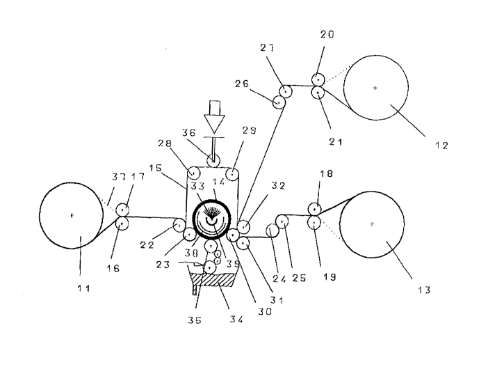
Fig. 4 shows a diagram of a device for replication and
~imultaneous application of a hologram to a printing
material.
2155~0
A printing material exhibiting a uniform surface
quality and which is drawn over a set of rollers (16, 17)
is on a roller (11). The printing material is guided over
the printing cylinder (14) via a further set of rollers
(22, 23), encircling the cylinder approximately 180 or
less. The printing material is then fed through a set of
rollers (30, 31), a further set of rollers (24, 25), and
between two rollers (18, 19) a winding roller (13).
If a carrier material is used, it can be fed as web
(37) through the application device together with the
printing material and wrapped onto the roller (12) via the
set of rollers (26, 27) and between two rollers (21, 22).
In order to increase the contact pressure of the
printing material to the printing cylinder, a belt loop
(15) can be guided over the surface of the printing cylin-
der (14) together with the printing material. The loop
encircles the rollers (23, 30, 29, and 28) and, if necess-
ary, can also be guided under the tension roller (36),
which regulates the web tension.
Via a spreading unit (34) with a spreading roller (35)
a lacquer layer is applied to the printing cylinder or,
alternatively, at a roller (23) onto the web which then
runs in between the roller (23) and the printing cylinder
and printing material encircling the printing cylinder.
The printing cylinder (14) is produced as a quartz or
acrylic glass cylinder (PMMA) and has a radiation source
21~ 5~
28
(33) in its interior, in particular a W-light source. In
order to direct the emission of light, a parabolic concave
mirror (39) and screens (38) are provided which can be
adjusted and regulate the area on the printing material
guided over the printing cylinder affected by the UV-
light.
In focussing the radiation on a more or less wide
strip or slit, the arc of wrap of the printing material
around the printing cylinder can be reduced corresponding-
ly-
The interior of the printing cylinder has a ventila-
tion device which feeds in cold air, on the one hand, and,
on the other, suctions off ozone.
In order to attain a high degree of efficiency, a
water-cooled pipe burner can be used.
As the lacquer applied via the spreading roller (35)
can be hardened by radiation, it already hardens during
the circulation of the printing material over the printing
cylinder to such an extent that it can be easily guided
over further rollers and can be wound onto the take-up
roller (13) or (12) respectively without the surface
structure being affected.
An electron radiation source with a suitable lacquer
system can also be used in place of a W-light source.
Common to the processes, however, is the fact that a rela-
tively liquid lacquer system is applied to the printing
21~850
29
material which can already be hardened without substantial
pressure during the shaping on the matrix. Where a W-
light source is used, this is achieved in particular by
the fact that the inventive printing cylinder and the
inventive matrix itself are designed to be W-light trans-
parent, so that hardening can be carried out from the
interior of the printing cylinder.
Fig. 5 shows an alternative device in accordance with
Fig. 4 in which a shape-bearing endless loop is used in
place of a printing cylinder.
The endless loop (40) can take up several micro-
structures or printing format lengths one after the other.
It is fed over the pressure cylinder (14) and a reversing
roller (41). This device allows matrixes to be changed
quickly in the printing unit. In addition, with this vari-
ation different printing format lengths can be easily
accommodated without changing the printing cylinder.
The spreading roller (35) applies the lacquer directly
to the endless loop (40). Otherwise, the device in Fig. 5
corresponds to the device in Fig. 4.
Fig. 6 shows a device consisting of several printing
units. The individual printing units correspond essential-
ly to the devices in Fig. 4 or 5. In a first printing unit
a primer is applied to the printing material in order to
smooth it sufficiently on its surface. The primer applied
can also be hardened by W-radiation.
2155850
The actual application of the micro-structure to the
printing material is carried out on the main printing unit
(46). If desired, a second printing unit (47) can be con-
nected, arranged in a reverse orientation to the main
printing unit and allowing for the back of the printing
material to be printed on.
In order to hold the web tension of the printing
material constant and to make it possible to correct the
longitudinal registers of the web, compensating rollers
(42, 45) are provided. A spreading unit (34, 48 or 49
respectively) is allocated to each printing unit.
Fig. 7 shows a diagram of the process to manufacture a
printing cylinder.
Right at the bottom is the glass substrate (54) with
the exposed and developed photoresist layer (53), which
contains the surface structure hologram. The UV-hardening
shaping medium is applied to the holographically struc-
tured photoresist layer (53).
This is done by spray casting (nozzle application
device, a number of proportioning nozzles with defined
diameters moves linearly over the plate), by immersion, by
spiral application, or casting and spinning.
The layer thickness should be at least 2 my and more.
- 21~3~3
31
A W-transparent acrylic sheeting or acrylic plate
(PMMA) is positioned (51) on the ~haping medium in close
contact to it as subsequent carrier of the shaping medium.
This plate or sheeting mu~t be flexible in order to
make easier detachment possible following hardening and to
facilitate the further assembly and reproduction steps.
A quartz glass plate (50), which is also UV-transpar-
ent, is positioned on the acrylic sheeting in order to
guarantee absolute flatness and close contact of the
acrylic sheeting (54) to the shaping medium (52) by means
of uniform pressure.
Preferably, this shaping or printing proces~ is
carried out in a vacuum printing frame in order to guaran-
tee optimal contact of the printing layer and to prevent
air bubbles.
Following the printing process by means of UV-expo-
sure, the acrylic sheeting is detached from the photo-
resist and either printed again for purposes of multiple
u~e copies (ganging up) or adapted to the negative shaping
cylinder.
This sandwich of acrylic and shaping medium is now
inserted into the interior of a negative receptacle (55)
which preferably consists of four shaping jaws linked to
one another via joints (56 - 58). After the negative shap-
ing receptacle (55) is closed, the shaping medium is
located within the hollow cylinder as "interior coating."
~l~S~5 ~
32
A quartz glass cylinder (54) is now inserted concentrical-
ly into the negative shaping receptacle (55). The relevant
process stage is illustrated in Fig. 7d.
Fig 7e shows the device to manufacture the printing
roller. A shaping lacquer provided in a tank (59) is fed
via pipes (60) into the space between the glass cylinder
(54) and photoresist (52). The filling of the space and
degassing is supported by a connected vacuum (61). The
shaping lacquer is hardened by means of W-light, an
appropriate light source being provided within the glass
cylinder (54).
After the shaping lacquer is hardened, the negative
shaping receptacle can be opened and the printing cylinder
(62) removed. The latter then bears on its surface the
micro-structure produced via the photoresist (52).
Following insertion of the printing cylinder (62) in a
printing unit, the actual printing of the printing
material can take place.
215585~
33
Reference number list
1 polyester carrier
2 separating layer
3 lacquer
4 metallization
hot-melt glue
6 carrier, printing material
7 lacquer
8 metallization
9 protective lacquer
cast finish
11 roller
12 roller
13 take-up roller
14 printing cylinder
loop
16, 17 set of rollers
18, 19 set of rollers
20, 21 set of rollers
22, 23 set of rollers
24, 25 set of rollers
26, 27 set of rollers
28, 29 set of rollers
30, 31 set of rollers
32 roller
33 radiation source
34 spreading unit
spreading roller
36 tension roller
37 web
- 215535~
34
38 screens
39 concave mirror
endless loop
41 roller
42, 45 compensating rollers
46 main printing unit
47 counter-pressure unit
48 application unit
49 application unit
quartz glass plate
51 acrylic plate
52 W-hardening shaping medium
53 photoresist
54 glass substrate
glass cylinder
56 negative receptacle
57, 59 joints
tank
61 pipes
62 vacuum connection
63 printing cylinder