Note: Descriptions are shown in the official language in which they were submitted.
21~96
MULTI-STAGE TRANSPONDER WAKE-UP, METHOD AND STRUCTURE
-
Cross-reference to related patents:
The following commonly assigned patent ~, o"s are hereby i"._u, ~u, dl
herein by reference:
Pat No./Seri~l No. Filina Date Tl Case No.
5 053 774 2/13191 Tl-12797
07/981635 11125192 Tl-16688
08/021 123 2123193 Tl-17529
Field of the Invention:
This invention generally relates to I t~coul ,i~iu" systems of the type which
include an i"~e, lù~udlul and a ~, dl l~pUI ,der and more particularly to such a system in
which the i"l~" U~dLùr transmits an i"~" U~dLiul1 signal to the l, dl ,~,.,u, ,.le, in
response to which the i"~u" U9dLUI transmits back to the i"~t,r,uud~or a response
signal. The invention further generally relates to improved methods of
20 communicating between the i, llul ~ U~d~UI and the ll dl Is,uOll~ l . In specific
embodiments the invention relates to an Automatic Vehicle Ide, lliricdliul1 (AVI) type
of It~u~lliliul1 system.
BACKGROUND OF THE INVENTION
The invention will be described in the context of an Automatic Vehicle
kJ~ iricdliul~ (AVI) system capable of exchanging data codes between an
i"le" u~udlul and a l, dl l::~pUI~ l . The AVI field is but ûne environment in which the
inventive concepts described herein can be applied. Systems using batteryless
30 l, dl ,spol1~e, ~ or ll dl ~ ~uullde~ ~ with batteries may be used for identifying or locating
Tl-1 8205
~ r
~1~599G
objects bearing the ~I dl Is,uolld~ such as cattle, luggage or other items Further, a
'` 1l dl ,~uondel might provide status i~ ~rul 1, Id~iUI I regarding the object on which it is
located, such as a ll dl ~pul~er born on a car door indicating whether that car door is
open Tl dl l::~pUI ~de~ ~ utilized in the above recognition systems or others may be
powered from batteries or from wireless radio frequency (RF) signals.
With respect to AVI systems, generally, the il ,L~" U~d~UI is provided in a tollbooth of a toll road, parking garage or other limited access facility. The il ,l~, r~u,dlUI
(reader) identifies passing automobiles by sending wireless il ILc:~ ~ U~dLiUI1 signals to a
I~d~,uu~1del (tag), which would normally be a small, self-contained unit placed, for
example, on the da~l lUOdl d or ~;. Id~ ld of the car. In this way the car (or other
vehicle or object) can be identified in a speedy and efficient manner Depending on
the use of the system, an account ~ or,i,ll~d with the driver, owner, or other
desi~, IdL~d person can be debited with an access charge. Compatibility standards
for one such AVI system is set out in Title 21, Division 2, Chapter 16, Articles 1~ of
the California Code of Regulations, herein known as the Caltrans ~ue~;iri~dliul~ or
Caltrans spec.
With respect to the specific ~ uodi~ l ll, which is cu" ,~dlil.le with the
2û Caltrans spec, the minimum role of the i~ 1 1 U~U,dlUI is to: 1 ) trigger or activate a
Il dllsluul 1~ 1, 2) i"l~" U9dl~:: the 1~ dl l::~UUI ,de, for specific il Irul " IdliUIl, and 3) provide
an ackno~ " l~l ,l message to the l, dl ~uul1 :1el after a valid response to theil llt~l I UydLiUI I has been received. The immediate mandate of the Caltrans spec
covers electronic toll collection, su",e~ill,es described as a part of =Electronic Tolls
and Traffic Mdl ,ag~" ,e"I" (ETTM) The AVI equipment for toll collection will typically
consist of two functional elements: vehicle-mounted ll dl IS,UO~de~ b and fixed-position
i"le" U~dl~
A toll collection site will consist of at least o~e i"L~ lugdlul operating in the
role described above. Upon i, IL~I, ugdLil lg or "polling" the L, ~"sL,u" ;lel for specific
Tl-1 8205 2
~13~9~6
il ~ru~ IdliUI I such as a ~, dl ,~uù,lder i ie, lliriUdliOIl ( ID) the i"L~" UUd~UI (or a separate
- computer) will typically check the Lldll~uulld~l ID against a database of valid non-
delinquent accounts. If the Lldllsuu,,d~:, ID is valid and non-delinquent the
il llt~l I U~d~UI will send a signal to a gate mechanism or a toll site computer operating
5 such a gate lll~.;l Id~ ", to allow the car to pass. OF course other e"ru~ u ~",e"~
means are possible that may ailow for less interruption of traffic such as allowing all
cars to pass and identifying the auto carrying the ~I dl ~uo~ l (or the rogue
automobile carrying an inoperable ~, dl la,uolld~l or no Ll dl ,~oll i~r at all) by other
means and notifying an dlJUIU~J~id~ rul t~ agency.
The i"~:, lugd~ion signal and response signal cûmprise data codes Caltrans
spec has set forth definitions for data codes to be ~Idll~llli~Led between the
ir~ luud~ul and the ~,d"spu"dtlr. The data codes described below are derived from
the Caltrans ~l~euiriud~iul~ and are merely exemplary and are intended to be neither
15 an exhaustive nor a mandatory list of codes for a general AVI system.
(a) Agency Code: This 16-bit code field identifies the Agency that has
authority to conduct the ~, dl ,sa.;Liu, ll
(b) Error Detection Code: The error detection code may be CRC-CCITT-16
20 with a generator polynomial of X'6+X'2+Xs+1. This results in a 1 6-bit error detection
code transmitted with each data message;
(c) Header Code: The Header is generally the first field in each data message
for either reader or ~ dl ,~u"de~ ~, dl l~l l ,issiu, ls and consists of an 8-bit and a 4-bit
word for a total of 12 bits. The Header provides a Uselsyn signal that may be used
25 by a receiver within a ~I dl ,~ur~ ~ ie~ or il l~t:, I o~dLul to self-sy,~,_l " u"i~e (selsyn) with
the data being received from the interrogator or ~I dl l~uoll it l respectively. An
exemplary selsyn signal might the binary and he,~dd~ I Idl values: 1 û101010 andM respectively.
(d) The Header Flag code provides for a unique 4 bit Flag that is, ~-u~ d
30 by a ~I dl l~uul I i~r or i, ,~l l Uyd~ul decoder as the end of the Header with the data
Tl-1 8205 3
2 1 5 ~ 9 ~ ~
message to follow. The exemplary Flag signal has binary and he~ddeuillldl values:
1100 and C respectively;
(e) ll ILt~l I uyd~ùr ID Number: This 32-bit field is used to uniquely identify the
i"l~lluydlur conducting the lld"sa~,liu,l;
(fl Tl dl ,:,auliu,l Record Type Code: This 16-bit code uniquely identifies a
specific type of valid ll dl ,sauliu,l between a reader and a L, dl I~UOl Id~r. This code
uniquely defines the ll dl ,~,uo, Icl~l message fields and functions penmissible. By way
of example, l1~dde.,i" Idl numbers 1 through 7FFF may be set aside for ll dl l~pl)l ,de,
message structures and 8000 through FFFF may be dedicated for
reader-to-tl dl l~pUI l~;;iel message structures;
(g) Trdl l~d-,l;on Status Code: Used to provide status i, Iru~ Illdliul~ to the
1, dl ~:~,uol1der; and
(h) Tldll~poll~ l ID Number: This 32-bit code uniquely identifies which
Il dl l~,UUI Ider is I e:"uulldil 19 to a polling request or is being dckl ~o~ ed.
Because the ll dl l~po,~de, ~ typical Iy either derive their operating power from a
small battery, or from a received RF signal, the 1, dl l~,uol~d~, ~ are not normally active.
The i"lelIU~dlul will transmit an RF trigger pulse to activate (turn-on) the
Il dl ISUUI Id~ i in d,UUI ua1~ li"g cars or other objects. The i, ILel I Uydlul may transmit a
number of RF trigger pulses at regular intervals to wake up any d,UUI uaul ~i"y
ll dl l~,UO~ Id~l ~. Altematively, the i"l~" uydlur might send an RF trigger pulse in
response to an external stimulus to the interrogator indicating that a ll dl ,~,uo"d~, is
dl~pludul lil 19 (e.g. Iight, heat, or magnetic sensors). After a time delay, the reader
then will transmit an encoded signal, referred to as the Polling message or
ill~llu~dliul-which, upon detection and decoding bythe lldl1s,uulld~l, will provide
initial i~ ~rù~ dliul~ to the transponder as to which data blocks the Ll dl l~uul ld~l should
transit.
In a descri~ed e,lluodil,l~ , the il l~til I ugd~ur transmits an unmodulated
3û continuous wave RF signal as an i, llt:l, uyd~ion signal to the ~, dl l::~,UUI ,~e, while
Tl-1 8205 4
21~99~
waiting for the L, dl l::~,Ub'l Id~l response signal. By analogy to acoustic signals, an
unmodulated RF signal is similar to a constant or "pure" musical tone without any
variation in amplitude or frequency. However, it should be r, Ib~ iUI led that a signal
could be bù,l~ide, .1 "unmodulated" in amplitude even if varying in frequency and
5 vice versa. The l, dl l:~pUI Id, :l response signal in this ~" IbObil I Ib~ comes when the
lldll~UUII~I b~chs,,;~llH~ modulates the continuous wave RF signal with i"rO""dliù,
frûm the Ird, lauol1dHI . Following the acoustic analogy, bdcksbdll~l modulation is
similar to the ~l lel~ul, Ibl 1011 achieved by singing into a fan and listening to the
resulting sound. Typically when a person sings, they control the variations or
10 modulations of their voice. Similarly, an RF 1, dl)~l I lillbr is generally able to modulate
its signal. However, when a person sings into a fan, the blades of the fan will reflect
the sound of the voice i"""edidl~ly back to the person when the blades pass
illllllebidltlly in front of his mouth. Thus, the singer hears a chopping sound
SU,Ub-l illluu5~d on his voice. That "chopping" sound the singer hears is nothing more
15 than the amplitude variation of the reflection of the sound of his voice. Similarly, the
Il dl l~UUI ,de, can modulate (by amplitude or other means) the continuous wave RF
signal received from the illl~llo~dlb, and this reflected signal will have modulations
sbue, i,~ ,,ubsed on it.
SUMMARY OF THE INVENTION
Disclosed is a system and method which conserves energy in the operation of
a 1, dl l::~UUI Id~l or tag by providing that the ll dl l:~,UOl ~del be enabled or awakened in
25 multiple stages. A threshold detector is provided which measures the power level of
received RF energy. If the RF energy received by the detector exceeds a pre-
dt:~l " ,i"ed level, the lldl l~pOI Id~r then employs a modulation detector to ascertain
whether it has been awakened by a valid i"~" U~dliUI I signal from an i, I~C!l, UgdlUl or
whether the RF energy received was merel~I a spurious burst of RF energy from
Tl-1 8205 5
~ ~ =
21~59g6
some other source. If a pre-d~l~rllli"ed modulation is detected by the modulation
detector, the 1, ar ~juùl ,der is then fully activated to its normal operational state.
This system and method further protects a ll dl lauul l~er or tag from being
5 enabled or awakened by spurious RF energy. A modulation detector is provided
which detects a modulation signal that is su,uel il ~ ,,uosed upon an RF modulation from
an irlL~I lU9d~UI . Preferably this s-~u~ illl,uused modulation is of a low frequency,
below those typically existing as Electro-Magnetic ll~l~l r~ ce (EMI), such that the
1~ dl Ispol Id~l is less likely to be erroneously activated by an U~ ded RF signal.
10 Upon reception of an RF illlulluudliull having the proper modulation su,u~,i,,l,uosed
thereupon, the modulation detector is operable to awaken other circuitry within the
1~ dl l~l)ol1d~l such that the ll dl ,~.u" ~ t is then operable to communicate with the
i~ ,tt" Ugd~UI .
Further provided is a system for communicating pe""d,~e"~ or semi-
pe~"ld"e"L i"ru""dliu" to a l,d~,~,uonde~ from an i~ u~dlur, preferably operated by
a toll agency or other authorized entity. This p~""ane"l or semi-pe""d"~"l
i"rul " Idliu11 is communicated by means of special instructions valid only during a
special mode or 1, Idil ll~:111dl IU.3 mode which is entered by 1~ dll~l l lillil l9 a special
20 access code to the 1, dl ,~uu".le, from the authorized i"l~" ugdlul . The 1, dl l~pUI lI.Iel
will preferably acknowledge to the authorized il IL~I, u~dlur that it is, in fact, operating
in the Illdil llelldnce mode so the interrogator can transmit the special instructions in
cùl ,ri.~ .e.
.
The preferred ~"l~o.li"~e~ ll of this invention further comprises a ll dl l~,uu~1de~
interface circuit that operates to allow communication between a l~ dl l::~,UUI n lel
controller and external circuitry. The interface circuit has a buffer memory which
allows the lldl ,~po,1d~l controller and the external circuitry each to transmit data at
either the l~ d"~pol1d~l 's or the external circuitry's clock rate without u~", '; ' ;1
protocols for direct communication. Each of the l, dl l::~,UUI ,de, controller and the
Tl-1 8205 6
~15~6
external circuit may be enabled by an interface controller to assume control of the
- buffer memory, including the clock circuit to the bufler memory. By using the buffer
memory and interface controller, whichever of the ~, dl l::~,UUI ,de, controller and the
external circuitry is ~ dl Ibl l lillil 19 or receiving data may fill or empty the buffer memory
5 at the clock rate of the 1, dl l~,UUI Id~r or the external circuitry. The interface controller
will monitor the transfer such that when the buffer memory is full or empty, theinterface controller will send a command to the dl.lJlUUI id~t~ transponder controller or
external circuit to either receive data from the full buffer memory or transmit data to
the empty buffer memory.
In the preferred e",uudi~ ,l of the present invention within a vehicle
travelling on a vehicle lane is a lldlla,uulld~l. The lldllblJol1dt:l receives the
i"'~,,uu~Liu" signal from the l,d"~",iLl~:r of the i"~"u~d~r and can reply to the
i"~t:l I U9d~UI by backscdL~r modulating a continuous wave input from the i
15 or another source. The receiver of the interrogator then decodes the backscd~modulated signal and may relay the i"rul1,IdLiulI contained in this signal to a control
circuit which, for example, might log the il ~rul Illdli~l, into a memory. A number of
Lldll~,uulld~l~ can be polled separately by ill~llUydlUI~ dssocidLed with each vehicle
lane.
The principles described in ,ul " ,e-_lio~l with this invention can be applied
toward r~on-AVI systems as well as AVI systems. For example, the power saving
principles described herein could be used with the inventions of commonly assigned
U.S. Patent No. 5,053,774 and U.S. Patent Appl. No. 08/021,123.
BRIEF DESCRIPTION OF THE DRAWINGS
In the drawings:
Tl-1 8205 7
-
21~5996
Figure 1 is a block circuit diagram of an i~ " U9dlUI and transponder
dl l dl lg~ l ll according to the present invention;
Figure 2 is a u~"e~ dli~d side elevation of a typical il l~alldliu" of an
5 Automatic Vehicle Ide~ l~iriCdliul I (AVI) System in a~ ddl IC~ with Figure 1;
Figure 3 is a ~r l~l dli~d top view of three adjacent traffic lanes using the AVI
System of Figure 1 the figure including a depiction of the timing sequence of a
trigger pulse and i, l~el I U9d~iUI I signal from the i~ l l U~dlUI to the ll dl l~pUI ,d~r
Figure 4 is a block circuit diagram of the ll dl l~,UUI ,de, and i"l~" UUd~UI
dlldll9elllellL usable in the systems of Figures 1-3;
Figure 5 is a more detailed block circuit diagram of the ll dl ISUOl ,~er of Figure
15 4 depicting a modulation detector a highpass filter and a wake-up block;
Figure 6 is an even more detailed block circuit diagram of the elements of
Figure 5 including the modulation detector the highpass filter and the wake-up
block;
Figure 7 is a timing diagram showing the signals at labeled nodes of the
l dl IS~UI l~ l as shown in Figures 5-6;
Figure 8 is a block circuit diagram showing the i"~e~ ;OI ll l~sC~iul I of various
25 function blocks of the Application Specific Integrated Circuit (ASIC) of Figure 5;
Figure 9 is a block circuit diagram of a receive buffer block preferably within
the digital Application Specific Integrated Circuii (ASIC) of Figure 8 for receiving
signal A from the modulation detect~r;
Tl-1 82û5 8
2155996
Figure 10 is a block diagram of the lane ~ i" ,i, Id~UI block preferably within
the digital ASIC of Figure 8;
Figure 11 is a block diagram of the main controller block preferably within the
5 digital ASIC of Figure 8;
Figure 12 is a block diagram of the main memory block preferably within the
digital ASIC of Figure 8;
Figure 13 is a block diagram of the transmit block preferably within the digitalASIC of Figure 8;
Figure 14 is a block diagram of the external interface block preferably within
the digital ASIC of Figure 8;
Figure 15 is a block diagram of the buzer block preferably within the digital
ASIC of Figure 8;
Figure 16 is a block diagram of the oscillator block preferably within the digital
20 ASIC of Figure 8;
Figure 17 is a block circuit diagram of an i,l~, IU-;~d~UI usable in the
~, a, ~uol1der and i, ,~, l U~d~Ol dl I dl Iy~l I ,enl: of Figures 1-3 wherein the i, ILt:l, UVUd~Ul is
capable of sending a low frequency modulation signal to activate the ~, dl IS,UO~
25 according to the present invention;
Figure 18 illustrate waveform graphs for two different e",L,odi",e"~ of
Usquitter modulation by which low frequency signalling from the i"L~" ugdLur of
Figures 14 can be suu~ uosed upon an RF i~ ~e~ ~ uudLiul l signal; and
Tl-1 8205 9
2~5~996
Figure 19 is a block circuit diagram of a Ll dl l::~,UUI ,de~ which also includes an
- RF threshold detector.
Co~ uol1dil 19 numerals and symbols in the different figures refer to
5 ~u"~suu".ii,~g parts unless otherwise indicated.
DETAILED DES~;hl. I ION
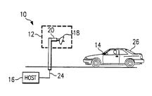
Figure 1 shows a block diagram of an AVI system 10 in which an
10 illl~llugd~ul 12cûmmunicateswitharemote~d~spù~der14bylldl,~,llillillgan
il IL~I I UUdliOI~ signal to the ll dl la,uul~del 14 in response to which the i, ~l~l l UrldlUI 12
transmits back to the illl~llUUdlUI 12 a response signal u ~IIldillillg a transponder-
unique identifying code (ID). In a typical AVI system the il ll~l l UU~d101 12 will convey
this ID code into a host computer (host) 16 for debit against the driver s account.
15 The AVI system 10 preferably includes il ,le, I U9dlUI ele- l, ul ,iu~ 20 for control of the
il ll~!l I U~dlOr 12.
Referring to Figures 2 & 3 multiple traffic lanes 28 are located at a traffic
control point such as a toll pla~a 29. Each traffic lane 28 has an as~ocidl~d
20 i"le"u~udlu, 12. The illl~llUUdlUI 12 maintains communication via an RF data link
with lldll~uul~d~l~ 14 carried on vehicles 26 travelling within the i,,le,,uudlu, s 12
dsso~idl~d lane 28. The illl~lluudlul~ 12 may have unique internal electrical
pdldlll~ such as illl~llogd~ul lane position illl~llu~dlor control pdldlll~ , and
i"t~" U~d~l reference frequency. The role of the interrogator 12 in this d~uliualiu"
25 is: to trigger or activate a Lld~l~uolldel 14 to i,,Le~lu~dl~ or poll the Lldll::~,UOll-.lel 14
for specific i"rul " IdLioll, and to acknowledge to the l, dl I~UI ,~el 14 that a valid data
exchange has taken place. As shown in Figs. 1-3 the i, IL~l l uydlul 12 has an
antenna 18 which is preferably mounted dU~JlU);illldlely 18 feet above the ground.
Preferably the antenna 18 will have circular pUIdl i~dLiUI 1, but advantages may exist
Tl-18205 1 0
21~ 6
which will motivate the use of other choices of pUIdl i~dliol) including linear and
ellipticai. I"l~"uudlur eleul,u"ics 20 are connected to the antenna 18 by suitable
cable, such as for example an RF coax 22.
The il ll~l l UUdlUI 12 communicates in a wireless fashion with the
l,dl l~,uu"der 14 by sending on/off keyed modulated signals to the ll dl l~UUI Id~l 14.
11 llel 1 U~dlUr 12 then sends a continuous wave RF signal to the ~, dl l~,UUI Ide~ 14. The
Il dl I~JOl ,d~r 14 may respond to the il ll~l l U9dLUI 12 by baCh:~CdlL~r modulating the
continuous wave RF signal such as described in U.S. Patent number 4,739,328 by
Koelle, et al. Details of the communication between the i~ lu~dlur 12 and the
,dll~,uol~der14willbefurtherdescribedherein. Thefunctionoftheoptionalhost16
is to control the ~peldliu"s of the ill~llU~,dlOI 12 and the peripheral functions of the
toll plaza. Such peripheral functions might include operation of traffic control gates
and other lane t:~ru~ue~le,,l equipment such as cameras and traffic lights. Still other
peripheral functions might include communications between i~ ugdlo~ 12 and
communications with a central office computer (not shown) that might maintain
account balance illru~llldliUII. Connection 24 between the ill'~llUU,dlUI 12 and the
host 16 as shown in Figure 1 may be an ethernet, token ring, RS232, RS422 or
other ,u"l l~-,Liull.
The interrogator 12 of Fig. 1 is housed in two modules: the electronics
module 20 and the antenna 18. As shown in Fig. 4, the ele.,llul,ius module 20
contains a Ll dl lall lill~l 52, a receiver 54, and a control circuit 56. The i~ UI~I ,ec-
tion 22 between the antenna 18 and the ~le~,~, u~ ,iu~ module 20 consists of a low-loss
25 RF il l~ UI Illt~UL, which is typically a coaxial cable, and a multi-conductor cable
capable of supplying power and control signal illrulllldLiu11.
Figure 2 shows a side view of a typical AVI system 10 il I~LdlldLion. In this
figure a vehicle 26 travels on a vehicle lane 28a-c and approaches the antenna 18.
Tl-18205 1 1
21~5~9~
A lldllapul~d~l 14 is located on or within a vehicle 26. Preferably the Lld"s,uol1der 14
- is mounted to the vehicle front window. In certain ,, ' ' ~s such as in unusually
large vehicles other locations such as on a truck's bumper might be dp,UI O,UI idl~:: to
reduce variation in height of ll dl ~a,uul1der 14. As shown in the figure, the vehicle 26
cdrrying the transponder 14 approaches the illlel~u~ddLu~ 18 at the toll plaza 29.
Further details regarding the communication between the ~IdllS,uu"d,3r 14 and the
l I U~d~UI 12 will be discussed herein. The UUI I l,UU~ a of the interrogator 12 and
lldl ,~,uu,~der 14 will also be discussed in greater detail.
Figure 3 is a top view of an AVI system 10 c~" ,,u, i~i, lg three lanes 28a-c. The
three lanes 28a-c are shown merely for illustration purposes; this system 10 could
be applied to one or multiple lanes. Preferably, circuitry is provided in the interroga-
tor12fordeL~,I,,i,li,,ginwhichofthelanestheL,~ ,uu,,:iel 14islocated. ClaudeA.
Sharpe's U.S. Patent Appl. No. û8/û21,123, assigned to Texas Instruments, provides
one such lane di~ulilllilldliol~ circuit and method.
Figure 4 provides a block diagram of the major cu" ,~,u, ~, ILs of the AVI
system 10. First, a Ll dl ~,uol~del 14 will be described with reference to Figure 4
together with Fi3ures 2 and 3. The AVI system 10 preferably c~",u, ises directional
antennas 18, each antenna 18 focused on an -~.s~ d vehicle lane 28a,28b,28c.
A vehicle 26 or vehicles 26 may travel on each lane 28a-c, each vehicle 26 carrying
one or more L,d"~,,uun,i~,~ 14. Each ~Idll~uulld~l 14 preferably cu"l,u,i~e:,. an
antenna 30, an analog or d"dlou/diu~ilal ASIC 32, a digital ASIC 34, and a modulated
reflector 41. Antenna 30 and modulated reflector 41 may form a single integratedantenna 311. Preferably ASIC 32 and ASIC 34 are integrated as a single ASIC.
With further reference to Figures 3 and 4, the Ll dl ~uul ll~l antenna 30 is
operable to receive RF Ll dl ,~" l;~iOlls from the i, IL~I Iuu~dLul 12. The analog ASIC 32
converts a signal supplied by the Ll dl la,uull ;1~1 antenna 30 to a voltage which upon
Tl-18205 1 2
21~9g6
exceeding a threshold activates the lldll::~pOlld~:l 14. According to the preferred
- ~"~bodi,l,e"L of the present invention the analog ASIC 32 senses high frequenGy
modulation present upon the signal from the ll dl IDUUI Idl~l antenna 30 and will only
activate the 1, dl ~uu~l~e~ 14 upon presence of that specific modulation frequency. In
5 this way the 1, dl ID,UUI ~der is relatively immune being awakened by spurious RF
Lldl~s",issiu,1s not UliUilldlill!J in the il~ lù~dlol 12 but only is activated when a
particularfrequency is lldll~lllilL~d bythe i,,l~D,,ugdlù, 12. The voltagethreshold
may be A~51 l~t~hle.
Preferably lrdllDluùlldelD14onlyrespondstoilll~llùgdliùllsignalsfromthe
10 ill~.lU~UdlU~ antenna 18a-c positioned within the lane 28a-c in which the vehicle 26
carrying the l~d~uu~lde~ 14 is travelling. To d~.UIlllJl;Dll this desired result when
the 1, dl IDlJUl~dUr 14 compares a first field strength pulse 44a received from the first
directional antenna 18a to a second field strength pulse 44b received from the
second dilDL;liUllal antenna18b. TheLIdllsuol~dlDr14maythenrespondtomessag-
15 es from the dU,UI U,UI id~fD il 1~1 l U~dLUI 12 (i.e. the i, llDI I U!Jd~UI A~so~ d with the lane28a 28b or 28c in which the ~I dl ID~UUI ll~lel 14 is travelling). A similar procedure will
be repeated between other lane pairs (e.g. 28a-28c 28b-28c). The tran-
sponder 14 is then operable to demodulate a i"le~,ugd~iul, signal which in the pre-
ferred e" ~uodi~ is amplitude modulated from the a~u, uu, id~ DI l Ugd~UI 12.
20 The ~I dl ,suond~-~ 14 is then operable to backDud~LfDr modulate a continuous wave
signal sent by the i, I~dl, uud~ur 12 to generate an response signal via a modulated
reflector 41.
Referring still to Fig. 4 the analog ASIC 32 and digital ASIC 34 typically
2~ process the ill~lluyd~k~l1 signal received from the lldll~lllilLIDI 52 and formulate the
necessary reply data. The digital ASIC 34 then provides the properly formatted reply
data stream to a modulated reflector 41. This ASIC 34 might be a simple digital
system using a fixed format or a more versatile digital processing system which can
i"~u, ~uo, d~D a number of options. Many options can be envisioned for the ASlC 34 to
Tl-18205 1 3
99~
ac..u",ul;sl, examples include but are not limited to: data storage data exchange
- history and battery capacity warnin0 The modulated reflector 41 is modulated by
changing its apparent wave length preferably between one fourth and one half thecarrier wave length. When the apparent wave length of the modulated reflector 41 is
1/2p, then the antenna 30 should reflect a large portion of the incident carrier energy.
When the modulated reflector 41 has an apparent length of %p it will reflect very
little of the incident carrier. As is well known in the art a switching of an antenna
between 1/2p and 1/4p can be ac~u"~ ed by ~u"~ le~ lg or disconnecting two %p
stubs. For the described l :lllI.o~il ll~l ,l the change in Reflective Cross Section
(RCS) is preferably between 45 cm2 and 100 cm2. By varying the RCS according to
the specified format data is sent from the ll dl l~,UUI ni~a~ 14 to the interrogator 12. The
lldll~7pUlld~ 14 are typically self-contained on a small credit card size assembly
that is completely portable. Preferably an internal battery is provided to give
operatingpowertothelldll~pol,.lel 14. Alternativelythel,d"sl~o,lde, 14mightgain
1 ~i its operating power directly from the RF signal. Although the modulated reflector 41
is described as a separate element from the ll dl la,uul ,cl~r antenna 30 it is possible
for both elements to be integrated into a single integrated antenna 31.
Now that the ~",~u"~"l~ of the l,d,)~onde, 14 have been generally de-
scribed in Figure 5 with further reference to Figures 3-4 a preferred e" Ibodi~ "el ,l
i~ ,le" U~dlUI 12 will now be generally described. The i, ,l~, l Ul~jdlUI 12 is located at a
specific point vlhere data exchange is desired such as a toll plaza 29. The AVI
system 10 may include a common reference oscillator 50 which generates at its
output 51 a reference carrier wave for S~ l ll u~ dliOI ~ of the i"l~, UUdlUI ~ 12. Each
illl~llu~dlol 12 has a directional antenna 18 and a 11d"s",ill~r 52 which transmit a
trigger signal 42 of sufficient field strength and/or modulation type at a pre-selected
distance to trigger or activate a ll a~ uol ,cler 14 being carried in a vehicle 26 in the
u~dlul s dssùuidl~d vehicle lane 28. The preferred e",l.o.li",~"l lldlla~ de( 14
Tl-18205 14
21 i5~
will be activated when a low power wake-up circuit 64 detects in the received signal
- a pre-selected modulation frequency.
Still referring to Fig. 5, if the wake-up circuit 64 receives the ul es-., iued modu-
5 lation signal, the wake-up circuit 64 will then apply clocks to the higher power
consumption digital ASIC 34. In this fashion power is conserved because the wake-
up circuit 64, which constantly monitors for trigger signals 42 (see Fig. 3), consumes
much less power than the digital ASIC 34, which is only activated upon detection of
a trigger signal 42 (see Fig. 3). After ll dl l~ lg the trigger signal 42 (see Fig. 3),
10 the illl~llugdlul 12 transmits an illl~lluydliol1 to the remote l,d"~uu"~er 14. The
il ll~l I Ugd~iO~l is preferably ll dl 1~ d using On-Ofl Keying. Upon .u, I l,ul~iul, of the
il llt~l I U~dLiUI 1, the 1, dl 1~ le~ 52 then transmits a continuous wave RF signal onto the
lldll~Uol~ l 14 so the lldll~,u~l1d~1 14 may bachsudll.3, modulate the continuous
wave RF signal to generate the response signal. The i"le" u~dlur 12 further
15 includes a receiver 54 for reception of the response signal and for S~Udl dliul1 of the
response signal from spurious non-modulated reflections. The i"l~l l ugdlùr transmit-
ter 52 and receiver 54 operate under control of a control interface circuit 56. The
host 16 byway of the control interface circuit 56 directs the lldll~lllillt:l 52 to send
the trigger signal 42, followed by the i"le~ I UU,dliUI I signal.
To allow proper lane di~ulilllilldliùll for a three lane scenario, a first interroga-
tor 1 2a, second i"l~" UgdlUI 1 2b, and third i,~l~l l U~dlùl 1 2c send simultaneous first,
second, and third i, ll~" ugdliol1 signals, respectively. During a first lane discrimina-
tion period 45, first i"ltn l U~dlUI 1 2a sends a first field strength pulse 44a and second
25 or third i, lltn ~ U~dlul ~ 12b,12c send no RF energy. During a second lane discrimina-
tion period 46, a second illl~,,ugdlur 12b sends a second held stren~th pulse 44b
while first and third i, llel 1 UUdlul ~ 12a,12c send no RF energy. During a third lane
d;~ ,l il l lil IdliUI I period 47, a third i"l~" UUdlul 12c sends a third field strength
pulse44cwhilefirstandsecondilll~luudlula12a,12bsendnoRFenergy Inthis
Tl-18205 1 5
21a~9~6
manner a l,d,~sl.onder 14 travelling in a vehicle 26 in one of the lanes 28a 28b 28c
Ac~c~ pd with each i~ o~dLul 12a 12b 28c can determine by culll~Jd~illg the
amplitude ûf the pulses 44a 44b 44c received during the first second and third field
strength periods 45 46 47 in which of the three lanes 28a-c it is travelling. The host
5 16 by way of the control interface circuit 56 is still further operable to direct the
Lldl ,~" ,ilLe, 52 to send the continuous wave RF signal following the i~ ILtn ~ u~dliul, and
to simultaneously direct the receiver 54 to receive the response signal. This
sequence can be extended to any number of lanes.
Theelectroniccu"~u~e~ 200fthe ill~llù~dLul 12will nowbe described in
more detail with respect to Figure 4. The ~le~ L~ Ul~iU~ 20 comprise a Ll dl ,~" ,ille~ 52
that is operable to send signals to the antenna 18 for the i"l~ lugdliul ~ of
transponders 14. Typically l,d,,a,,,ilL~I 52 receives signals from the host 16 via the
host ~u", le- liul1 24. During the ll dl l~ul~d~l reply the ~I dl ,~",ill~r 52 transmits a
15 continuous wave RF signal to the Lldl~uul ~der 14 which then backscdllt:r modulates
the continuous wave RF signal with the reply data. The receiver 54 detects the
reflected energy which is ~ackscdLl~, modulated by the ll dl ,~ u"d~r 14 and sepa-
rates the modulated signal from the non-modulated reflections. Antenna 18 shown
here in electrical communication with the Lldl l~lllilL~I 52 and the receiver 54 is a
20 .li, ~-.Liu"al antenna 18 with a precisely shaped pattern and is used to radiate and
receive RF signals covering a portion of each lane during the data exchange be-
tween the i~le~uydLul 12 and the lldl1~Jul~d~l 14. In the described embodiment asingle antenna 18 is used for both the i"L~" UUdLio~1 signal and the response signal.
The antenna 18 is typically mounted d~UUlU~illldL~Iy 18 feet above the roadway and
25 is preferably posili-)"ed to ensure a constant link between the il ,Le" ugdlu~ 12 and
the lldlls~ol~d~l 14 regardless of site-d~ elld~,ll variations. Also shown is the
control circuit or host interface 56 used to communicate with the host 16 which may
control all the il ,L~, ru~dlu, ~ 12 at a single toll plaza.
Tl-18205 1 6
2 ~
Still referring to Fig. 4 the host interface 56 between the i"le"uydlu, 12 and
the host 16 for certain read/write ùuerdliù"s accepts il ~rul " IdliOll from the host 16 via
the host connection 24 and formats the data for ~I dl 1~ iUI I to the vehicle 26 by
means of the lldl l~,,,ill~l 52. Preferably the communications with the host 16 will not
occur until after the lldllallliLL~, 52 has uulllult:l~d an entire read/write L~d~sauliull
with a ll dl l::~UUI 1~.1'3r 14. The host interface 56 also decodes the reply data from the
Ll dl l~,UUIld~l 14 by means of the receiver 54 and supplies this reply data to the host
16. The antenna 18 is preferably v.~ ,el ulùof and designed to operate over the
dl ILiUi,Udlt'l;;l temperature extremes in its environment.
Referring now to Fig. 4 in light of Fig. 3 for multiple lanes one i, llt,l lU9dlUr 12
will preferably be provided for each lane. All il ll~llug~ul~ 12 at a toll location 29 will
be ~uo, .li, Idl~d in frequency power output and antenna pattern to minimize overlap
of coverage and il ~le~ ru~ ellce between adjacent lanes. A different carrier frequency
is typically used in each illl~lluydlul~ 12. Alternatively adjacent interrogators 12
might have differing carrier frequencies to minimize i"l~rr~r~,lue as between the
adjacent illL~IIuudlul~ 12 while non-lleiyl,uo,i"g illl~llUydlUl i might use the same
carrier frequency (i.e. where the interrogators are arranged spatially as #1 #2 #3
#4 #5 and#6 illl~loydlul~i#1 #3 and#5mightuseonecarrierfrequencywhile
i"l~" Uyd101::~ #2 #4 and #6 might use another carrier frequency). A common carrier
frequency might be used in all illl~llugdLul~ 12 such as in a system which provides
lanedi;,l,,i,,,i,laiLollbetweenLId,,~pu,,d~l~14asasdescribedintheco-assigned
Sharpe U.S. PatentApplicatiûn No. #û8/021 123.
The receiver 54 of the i"le~, UydlOl 12 detects the bduk5~,dlL~I modulated
return signal from the L,d,~suu,~d~r 14. The amplitude and phase of the return signal
will be completely dep~l Idul ,L upon the multitude of I ~rleuliu"s which occur from a
number of sources. Undesired sources of return include the following: vehicles 26
in the same lane as the i"L~ lo51dLul 12 creating beamfilling or non-beamfilling
Tl-18205 1 7
21~996
unmodulated returns; vehicles 26 in adjacent lanes 28a,28b,28c creating
unmodulated and L,auhs~d~l~, modulated returns; fixed obstacles of unknown
,ulll,uu~iliùll creating unmodulated returns; and leakage from the l,d"~,l,ille, 52 to
the receiver 54 during lldl lal "i~sio,~ of the continuous wave RF signal to the5 lldll~ JUll~i~l 14.
Typically, one i"~el,u~dlul 12 is provided for each lane 28 in which a data linkis to be enabled. Furthermore, except for site-u,u~,all""a~le internal electrical
pdldlll~l'i such as lane location, orothercontrolled pdldlll~ 7, all illl~lluy, .~UI5 12
10 are identical and are coordinated in time by a common reference oscillator 50.
The cu" ,,uune"I:, of the analog ASIC 32 and the digital ASIC 34 will now be
described in greater detail below.
15 WAKE-UP BLOCK:
With reference to Figure 5, a more detailed diagram is shown of the analogy
ASIC 32. The interrogation signal is received in the analog ASIC 32 from the
antenna 30. The modulation detector 70 acts to remove the carrier signal from the
20 received interrogation signal and pass this to the first stage circuitry 62. The first
stage circuitry cOI ~ I,ul i~s a lowpass filter 72 which removes high frequency
uu"~l~u"e"~:, of the signal from the modulation detector 70. The output of the
lowpass filter 72 is further transmitted to a threshold detector 68 that compares the
output of the lowpass filter 72 to a reference voltage. The output of the threshold
25 detector 68 will thus be a binary signal which will be an input signal, djnl to the digital
ASIC 34 and to the wake-up circuitry 64.
With further respect to Fig. 5, the inventive concepts described herein have
significant advantages over the prior art in terms of power consumption. It is of
Tl-18205 1 8
21~9~
signihcant i,~ ,uu, Idl n.e tû design a ll dllS,UUI Id~l 14 that consumpes minimal power.
The illIIJIIdl,ce ûf a power-efficient lldll:~JUII~ 14 exists whether the tran-sponder 14 is powered by a received RF signal or whether the the L, a, ,~I,u, Ide~
operates on a battery. By i",IJle"~t:"li,lg the inventive concepts described herein, the
5 ~Idl l::~,UU~ el 14 wiil normally be in a sensing mode with a 1/24 duty cycle sleep
mode, drawing little energy from the battery or RF energy source. The only energy
consumed in this duty cycle sleep mode will be that required by the wake-up circuit
64.
Still referring to Fig. 5, a high pass filter 74 is provided at the output of the
detector 70 to hlter out any spurious low frequency signals such as from cellular
phones or other sources. The high pass filtered signal is provided from the filter 74
at node "D." The filter 74 may alternatively be a band pass filter. In an alternative
~ uodi,,,t:~lfilter74maybealowpassfilterwhenthel~d~suollderisactivatedbya
15 low frequency (LF) modulated signal. Upon detection of an RF modulation of the
frequency of interest by modulation detector or pulse counter 78, the wake-up
circuit 64 sends an enable signal, "F," to OR gate 97 which will in turn send a
wake up signal to the digital ASIC 34 so long as either "Fnthe clock signal to the
digital ASIC 34 to enter an active state. In a first preferred ~",uoui",~, Il, the
20 expected modulation frequency will be the high-speed modulation of dU~JlUAlllldl~ly
100 kHz to 4û0 kHz. In another preferred erl ,uo~" I l~l ll, a low frequency signal of
below d~,uluAillldlely 1000 Hz is suue,il"uosed upon the 915 MHz carrier and this is
the modulation signal expected by the pulse counter 78
In further reference to Fig. 5, for the first preferred e,lluo.li,l,e, Il, the pulse
counter 78 is preferably a gated 5 bit counter circuit. The gate is set at a specific
frequency so that a range of valid counts is detected. To further save power, the
wake-up circuit 64 has its power duty-cycled. For example, every 16 ms, a 2 ms
window might be opened (1/8 duty cycle), and within the 2 ms window the detector
Tl-18205 19
215~9~
might be on for 62.5 us and off for 125 us (1/3 duty cycle). This example of
- duty-cycling (1/8 x 113 = 1/24 duty cycle) would effectively reduce the power
consumption to 1/24th of the original value.
Referring now to Figure 6, the wake-up circuitry 60 is shown in still greater
detail. If modulation is detected, the digital ASIC 34 is activated and the pulse
counter 78 is kept active by an "assert" signal from the main controller block 140
(see Fig. 11 ) of the digital ASIC 34. If the modulated RF signal .li~c,,upedl ~, the main
controller block 140 by the "assert" signal may keep the wake up signal from OR
gate 97 active until the digital ASIC 34 functions are completed. The main controller
block 140 will not disable the wake up signal From OR gate 97 until all pending
functions are completed.
Still referring to Fig. 6, the detector 70 preferably comprises a diode 82 whichreceives and rectifies the signal at node "A" from the antenna 30. A shunt capaci-
tor 84 and shunt resistor 86 act to form a low pass filter having a known time
constant so that the 300 kHz .~ ,l ,esl~r modulation can be extracted from the ~15
MHz continuous wave RF signal. A high pass filter 74 then acts to filter out any~"d~ dLI~ low frequency cu" ~uunel ,l~, The high pass filter 74 ~u" ,,u~ ises a series
capacitor 88 and a shunt resistor 90. It is important to u, Id~l ~Idl ,.i that the
.,u" ~,uull~l 11 values of the detector 70 and the high pass filter 74 are selected
de,o~ ,u on the modulation frequency that must be detected to enable the digitalASIC 34 by signal "F", (Fig. 4). In other words, the high pass fllter 74 may have a
very low corner frequency or may be ~',."i, I~L~d altogether if the wake-up circuit 64
is expecting a modulation frequency that is lower.
With further reference to Figure 6, gated ~u" lua~ dLul 92 receives clock signals
from the pulse generator 76 on node "E." The input from the pulse generator 76
serves to gate the voltage pulses from node "D." Thus/ if the input from node "D"
Tl-18205 20
21~996
(flowing from high pass filter 74) is the correct modulation frequency gated latch 96
serves to provide a high input to an OR gate 97 that performs a logical OR of the F
signal and an assert signal from the main controller block 140. The F signal is
asserted once the correct count has been reached and until the falling edge of the
5 gating pulse from the pulse generator 76 resets the gated latch 96. The gated
latch 96 serves to provide a high input to a OR gate 97. Depending on the signalfrom the gated latch 96 or an ext assert signal from an external ~ u~unl~oll~
the output of OR gate 97 provides a wake-up~ signal to the digital ASIC 34 (see Fig.
5)
Referring now to Figure 7 a timing diagram for a preferred ~" Ibo.li,"e"l
modulation detector is shown. The signal at node D is shown as a continuous
wave 915 MHz signal with 300 kbps Mdl ~ e~Ldr 11 On-Off Keying (OOK)
supel il "uùsed Bursts of 300 kHz modulation occur on the signal at node D as the
15 high pass filter removes the 915 MHz carrier signal from the node A signal Atnode E is the gated latch output which exists with a certain duty cycle when
modulation is detected by the wake-up circuit 64. The wake-up signal is the output
of OR gate 97.
Figure 8 illustrates an overview of the functional blocks 10010811401
14815517211901214within an e",uo~i",e~l of the digital ASIC 34. Within the digital
ASIC 341 a clock block 214 receives a wake up signal from the analog ASIC 32 andthereupon begins to generate clock signalsl preferably at 3 6 MHz 1 2 MHz û.6
MHz and 0.3 MHz These clock signals are 1, dl lalllill~d to the above functionalblocks including at least the main controller block 140 The clock block 214
preferably continues ~ell~,dLiull of the clock signals I~Z~dl~l~SS of the status of the
wake up signal received from the analog ASIC 32 until receiving a clk disable
signal from the main controller block 140 Once the RF signal level is removed and
the main controller block 140 is in the idle state (i.e the main controller block 140
Tl-18205 21
21~995
has completed all its necessary D,OeldLio~ ), it will signal the clock block 214 via the
- clk disable signal and 0.5 ms later the clock block 214 will disable oscillation of all
the clocks. The digital ASIC 34 will remain deactivated until the next RF signal of
proper level is detected and the analog ASIC 32 sends another wake up signal.
5 The nature of CMOS digital logic is that it draws power only when changing states,
or to a lesser degree when it is being simply being clocked; therefore, the static
current drain of all the digital CMOS logic with the clocks will be very small (in the
nano amp range).
Still referring to Fig. 8, the receive buffer block 100 receives a data-bearing
signal, djr~ from the analog ASIC 32. The receive buffer block 100 decodes this
signal autonomously from the main controller block 140 and is operable to transmit
received data to the main controller block 140 or to main memory block 148. The
decoded signal can be received by the main controller block 140 without buffering
15 via the signal, incoming data. Alternatively, the decoded sinal can be stored and
buffered in the receive register 122 (not shown, see Fig. 9) and accessed by themain controller block 140 sending an address signal radr 11. The data output
rdat 11 of the receive register 122 (see Fig. 9) may be received directly by the main
controller block 140, or it may be received by the main memory block 148 for storage
20 therein. The receive buffer block 100 preferably also provides an incoming msg
signal to notify the main controller block 140 that an i"l~" UydlkJ~ I is being received.
Furhtermore, the receive buffer block 100 may provide a msg valid signal to the
main controller block 140 to inform it that the interrogation was received without
received error. The receive buffer block 100 also might provide a signal,
25 manch active, to the lane ~is-,, i" ,i, Id~iOI~ block 108 to notify the lane dis-., i" ,i, IdliDIl
block 108 that the receive buffer block 100 is actively decoding the data-bearing
signal. din.
Tl-1 8205 22
21~9~6
With further reference to Fig. 8, the lane dis~, i"~il IdliUI~ block 108 is operable
- to receive djn and manch activity and determine in which vehicle lane 28 (Fig. 3~, the
vehicle 26 is travelling. The details of this lane ~ ;, i, l ,i, IdliUI- block 108 is described
more fully below and in Claude A. Sharpe's U.S. Patent Appl. No. û8/û21,123,
5 assigned to Texas Instruments. The lane di~ i,ni, IdliUI1 block 108 upon
dtlll~!llllilld~iUII of the vehicle lane 28 (Fig. 3) in which the vehicle 26 (Fig. 2) is
travelling, may transmit this i~rul Illd~iUIl to main controller block 140 as the signal,
lane #.
The main memory block 148 shown in Fig. 8 is operable to store data
received from the receive buffer block 100 as ",e"liuned above. Further, the main
memory block 148 is operable to receive data from an external "li~,~ UCol l~ (not
shown) via the external interface block 172. This data exchange is via the
a~d, t~ssi"g signal, radr 22 and via the data signal, rdat 22. The main memory
15 block 148 may also receive data sent from the external ",i.;,u~u"I" 'IF (not shown)
via address and data signals, I~C adr and ,uC dat, respectively. The main memoryblock 148 is may be enabled or disabled by the main controller block 140 by the
select signal. The external interface block 172 operates as an interface between the
main memory block 148 and an external " ,iw ocu"~" '' (not shown). The external
interface block 148 receives an enable signal from the main controller block 140 and
a clock signal from the clock block 214. Preferably, the clock signal is 1.2 MHz. In
this ~"~uodillle"~, the external interface block 172 communicates with the external
IlliwucullIl~ 'I (not shown) by a serial clk signal, a serial l/O signal, and a number
of lldl l~l Idkil ,9 signals (,uC rdy, R IW, and ext assertj which will be described in
more detail in the d~s~ Jliul I with respect to Fig. 14.
A transmit block 155 is also shown in Fig. 8. The transmit block 155 operates
under control of the main controller block 140 to transmit data in a response signal to
the irllt:lluydLur 14 (not shown, see Fig. 1) by preferably ~a,_hs~dl~er modulating the
Tl-18205 23
215~9~6
data upon a continuous wave RF signal from the i"L~ ~ U!Jdlul 14 using backs. dlL~
- modulator 41. The transmit block 155 receives data from the main memory
block 14~ via the data signal rdat 21 and add,~ss~s the main memory block 148
using the address signal radr 21. The transmit block 155 communicates with the
5 maincontrollerblock140usingsignals(xmit data select start xmit complete and
trans count) which will be described in more detail in the .lesu, iuliol1 with respect to
Fig. 14.
A buzer block 190 shown in Fig. 8 operates to transmit indicating tones to an
operator via a buzer 212. The buzer block 190 operates under control of the maincontroller block 140. The main controller block 140 sends control signals beep type
beep enablel beep start to the buzzer block 190. These Gontrol signals will be
described in more detail in the des.;, iuliu" with respect to Fig. 15.
With further reference to Fig. 8 upon co" ~ liul I of a successful ~ d~;liu
comprising an il ,le" ugdliol, and a response in which no data errors occurred the
~I d~ l~,UOl Id~l 14 for example might enter a 10 second period during which it will not
respond to further i~ " U9dliU11~ having the same agency code as the just-
d l~ d~l~a~liu~ u~dlio~ ~s received during this l lul ll ~lJo~ e period
20 be compared to the previous agency code and will not be responded to if the
agency code is the same as the previous agency code. If a different valid agencycode is received during the llu~e~l~u~ive period the l,d"~po"de, 14 may respond
to the new interrogation.
25 RECEIVE/BUFFER BLOCK:
Referring now to Figure 9 the ~o" ~uu~lel 1~ of the receive buffer block 100 of
the digital ASIC 34 will be described. The receiver block 100 contains a Mdl lul le5
decoder 102 CRC-CCITT calculator 106 and a state controller 110. The receiver
Tl-1 8205 24
21~599~
block 100 will decode ~ld~ llissiu~ls from the i,,te,,ugdLur 12, determine in which
lane the Ird"~po,1del 14 is located, and calculate the incoming ~essaue'~ CRC. The
1\~ ,uI,e:,~e, decoder 102 receives data-bearing signal, djn/ from the analog ASIC 32.
The Md"~ e~l~r decoder 102 comprises a digital phase-locked loop at 3.6 MHz to
5 enable the Mdn-:l ,esl~r to synchronize to djn The Manchester decoder 102 provides
at its output a received serial data stream, SRDT, and a clock signal, SRCK, derived
from the data-bearing signal, djn The l l Idl ll,l Irj~len decoder 102 also provides a
manch activity signal to the lane ui~u, il"i~ IdliUI, block 108 (see Fig. 8). The purpose
of the manch activity signal will be later described with respect to Fig. 1û.
Still referring to Fig. 9, the serial data stream, SRDT, is fed into a CRC
generator 106. The CRC of the incoming message is calculated using the CCITT
polynomial (X16 + X~2 + X5 + 1 ). The receive controller 110 determines which data
bits are calculated in the CRC (the overhead bits are not calculated as part of the
15 CRC) and activates the CRC generator 106 to begin calculating the CRC after the
overhead bits have all been received. A byte counter 114 is provided to receive the
serial data stream and count the number of bytes received. The number of bytes
may be counted by ir IUI ~1 1 lel 11il l9 the byte counter 114 with every eighth pulse of the
serial data clock and 1, dl l:~l l lillil IvU the count to the main controller block 140 (see
20 Fig. 8). An eight-bit holding register 116 is provided for holding bytes as they are
lldll~lllill~d from the serial-to-parallel shift register 112.
A data 1O1ll~Jdldlur 120 is provided so the receive controller 110 can compare
data from the serial-to-parallel shiff register with that stored in a SRAM 118. In this
25 manner, for example, the ll dl ,pu"del i~ie"liricdliu,1 might be stored in the SRAM 118
and compared to an ID code gleaned from the serial data, SRDT by the receive
controller 110 via the serial-to-parallel shift register 112. Thus the receive buffer
block 100 operates autonomously from the main controller 104. The receive control-
ler 110 senses received 1\~ IuI,e~L~-encoded data on the manch activity line from
Tl-1 8205 25
21~99~
the Mdl l-,l ,e~er decoder 102. The receive controller 110 is further operable to
- bypass the CRC generator 106 or to reset the CRC generator 106 using control lines
crc bypass and crc clear. Upon sensing the start of reGeipt of Ma,1,.1 ,e~l~r-encoded
signals, the controller 110 preferably resets the CRC generator 106 and resets the
5 byte count register 114. The Gontroller 110 may control the receive register 1Z2 to
store data from the eight-bit holding register 116.
LANE DISCRIMINATION BLOCK:
Referring now to Figure 10, the lane di;,u~ dlion block 108 includes a lane
.lis.;, il I lil Id~iUI I controller 124 that samples at three specific times after the
ir ~le~ ~ U~dliul, of the Ll dl l~,uu~ r 14 by the il ll~l I u!Jdlur 12 is initiated (see Fig. 3).
The lane di~ i",i, Idli~l, controller 124 stores voltage samples from node "B" of the
analog ASIC 32 (see Figs. 5, 8) in capacitors 126a, 126b, 126c, whose voltages be-
15 come inputs to an voltage UUlll,UdldlUl/deUOder 130. The lane uis-.lilllilldlio~l
controller 124 samples node "B" during sample periods 45,46,47 (see Fig. 3) to
sample field strength pulses 44a-c (see Fig. 3). Switches 132a,134b,132c connectthe capacitors 126a,126b,126c, respectively, to the node "B" input voltage (see Figs.
5, 8). The output of the UUIll,Udl d~UI 130 is sampled a specific time later (after
20 settling) to determine which signal was stronger, and therefore in which
lane 28a,28b,28c the ll dl l~l~u"de~ 14 is located.
Still referring to Fig. 10, the lane ~ ul i" ,i, Idliul, block 108 is preferablyautonomously operable to sample the field strength pulses without need for supervi-
25 siûn from the main controller block 104 (see Fig. 8) or other uo"L,-" ~. The lane
Ui.~lilllilldliUI~ controller 124 receives the manch activity signal from the Receive
Buffer Block 100 (See Fig. 8). Upon the detection of Mdl l-,l ,e~ , encoded signals
(manch activity = high), the lane .lis, ,il"i"dLion controller 124 starts a long timer 138
to await the u~ iul ~ of the incoming interro~ation (see Fig. 3). After the long
Tl-18205 26
996
timer 138 has c~" Iul~l~d its cycle the lane .li~-;l i",i, Idliul, controller 124 begins to
monitor the node ~B" voltage for field strength pulses 44a-c (see Fig. 3). A short
timer 137 provides 3.3 us sample timing between the pulses. Using this 3.3 us
timing the lane dis~,i",i"dliu,~ controller 124 is properly syl1.;,u~ d to the sample
periods 45 46 47 (see Fig. 3). It should be u"de, ~luod that the timing periods
described above are merely exemplary and that other periods may be used
depending on system design pdl dlll~el 5 such as the number of lanes being
~iauli",i"dled between and the length of the il~ llu~d~iul1 and timing pulses.
MAIN CONTROLLER AND COMPARATOR BLOCK:
With respect to Figure 11 the main controller block 140 controls the overall
actions of the digital ASIC 34. The main controller 104 is awakened by the "wake-
up" signal from the analog ASIC 32 (see Fig. 8). The main controller 104 then
makes decisions based on the incoming message content and the current
l,d,lsa- liu,l sequence. The Cullludld~ùl 142 takes the incoming messages from the
receive buffer 122 verifies the validity of the received message using the calculated
CRC and performs ;Ulllp~li51~ 5 on the incoming message i~ru~ dliul1. The main
controller 104 executes the dUpl uu, idLe command sequence.
Still referring to Fig. 11 a Record Type Code (16 bits) of the incoming interro-gation is used to determine the order and type of UulllUdl i50115 performed. This code
uniquely defines the 1, dl ,suu"del message fields and functions pe""i~sil,le. By way
of exampie ll~xd~aui" Idl numbers 1 through 7FFF may'be set aside for lldl l~pUI Id~l
message structures and 8000 through FFFF may be dedicated for
reader-to-l, dl la,uOl~ l message structures. Affer the i~ l l UUd~iO~1 has been tested
for data errors using its CRC the Record Type Code is examined and the
c~, I lUdld~UI circuit 142 sets flags in acuu, ddl ,c~ with the Record Type Code. The
main controller 104 acts upon the flags generated by the ~u",ua,d~u, circuit 142 and
Tl-1 8205 27
21~ 6
takes the d,U,UlU;JI id~e? actions to analyze the data content of the il ~Let~ uudliol ,, to
- generate the data for the Ll dl IS~Ollelt:l '5 14 re ~,ùul ~aes, and to signal the optional
external ~ u-;u~L~uller (not shown) or to perform ASIC l~ai~e?~d~ce functions
(discussed below under the heading "MAINTENANCE MODE AND MESSAGES").
The main controller 104 also acts to load the main memory block 148 (see Fig. 8)with i~rulllldliUIl by providing ad.l,~sses to the main memory block 148 in which to
store data. Typically the source of this data would be the received il l~l, UUdLiUI I or
the external I l lie,l u~u"ll ~ " ?, (not shown).
With further respect to Fig. 11, ll dl ,sa,.;Liu, I counter 146 is an 8 bit counter
which is il IUI ~ d at the end of an ackno~ dull~e l ,I message from the
il llel I U~UdLUI 12 (see Fig. 1 ) if the ll dl ~sa.,liol1 was successfully uu, ~ ldd (e.g., the
i, lle?l I U9dlU1 12 received a valid ID code from the 1~ dl l~ul1dul 14). The 1~ dl ,:,a,.liol1
counter 146, though part of the main controller 104, is add,t,sse~ within the address
space of memory block A. The ll dl ,~a,,li~l~ counter 146 provides a circulating 8 bit
number which can be used to track successful toll Ll dl Isae;Liul~ and Illdil llel lance?
operations for boukkee,ui"~ purposes (much as a "check number" keeps track of
personal bank ll d,~sa-;liul Is). The value of the ~l dl Isa-;liùl I counter is not normally
programmed, but may be reset to ~ero by resetting the ASIC via the external reset
pin or by another method.
As can be seen in Fig. 11, in addition to performing functions relating to the
receipt and processing il IL~I lu~dliun messages, the main controller 104 acts
somewhat as a nerve center for the 1, dr ,~I ol~der 14. Many of the control signals
pass to and from the main controller 104 to the other function blocks 100,108,140,
148,155,172,190,214. The main controller 104 receives its timing from the
exemplary 3.6 MHz clock from the clock block 214. The clock block 214 preferablycontinues ~Je,1~ldliul ~ of the clock signals, 1 ~dl~less of the status of the wake up
Tl-1 8205 28
21559~
signal received from the analog ASIC 32, until receiving the clk disable signal from
the main controller 104.
Still referring to Fig. 11, the main controller 104 may receive data from the
receive buffer block 100 either withoui buffering via the signal, incoming data.Alternatively, the decoded signal can be stored and buffered in the receive
register 122 (not shown, see Fig. 9) and accessed by the main controller block 140
sending an address signal radr 11. The main controller 104 is also operable to
store data in main memory block 148 by sending address signal wadr 21 and by
enabling main memory block 148 by the "select" signal. Main memory block 148,
once so selected, wiil be operable to receive data directly from the receive buffer
block 100 by signal rdat 11. The receive buffer block 100 preferably also provides
an incoming msg signal to notify the main controller block 140 that an i"Ie~IugdIiul,
is being received. Furhtermore, the receive buffer block 100 may provide a
msg valid signal to the main controller block 140 to inform it that the il ,~e, I ug~iu"
was received without received error.
With further reference to Fig. 11, the main controller 104 receives a signal,
lane #, from the lane ~ia~ iUII block 108 to determine in which vehicle lane 28
(Fig. 3) the vehicle 26 bearing the I,~"al.o,~de, is travelling (see Fig. 2). The
transmit block 155 operates under control of the main controller block 140 to
transmit data in a response signal to the i"L~" uy~Lul 14 (not shown, see Fig. 1 ) by
preferably bauh~ d~le, modulating the data upon a continuous wave RF signal fromthe il lI~l l UgdtUI 14 using baGksc~lL~I modulator 41. The transmit block 155 receives
data from the main memory block 148 via the data signal rdat 21 and addresses the
main memory block 148 using the address signal radr 21. The transmit block 155
communicates with the main controller block 140 using signals (xmit data select,start, xmit complete, and trans count) which will be described in more detail in the
d~su, ilJliul, with respect to Fig. 14. The main controller 104 controls the buzer
Tl-1 8205 29
21~9~
block by control signals beep type, beep enable, and beep start. These control
- signals will be described in more detail in the description with respect to Fig. 15.
MEMORY BLOCK:
The main memory 150 shown in Fig. 12 has memory blocks A, B, C, D and
M. Preferably, each of the exemplary five blocks of memory is available for
~I dl lal I ~is~iùl, to the il ,~ U~dLUI 12 by the transmit block 155 (see Fig. 8). The
memory 150 is preferably a multi-port SRAM, allowing simultaneous read and write10 u~Jeldliùl)s. Preferably memory 150 is a SRAM having a capacity of 8û bytes,
however, memory 150 might be non-volatile memory (e.g., EEPROM, ROM). Fur-
ther, memories having more or fewer than 8û bytes could be i~,ulerl le, I~d in an AVI
system or other systems in a,,-;u, ~dl ,.,e with this invention.
Still referring to Fig. 12, the selection muxes 152,154 allow writing to the
memory from the main controller 104, from the external I I ~iu~ u-:ul lll uller (not shown)
through the external interface block 172. Through the i"~"u~d~iun message, the
i"~e" UUd~Ul 12 may ask the l, dl ,~ dt,r 14 for a 16 byte data ~I dl 1~11 ,issiul ~ of
msmory block A, B, C, D, or M. As an alternative, the i"le~, uudlioll message might
instruct the transponder 14 to send a longer burst of data, such as 32 byte datatransmission. For example, a 32 byte data l, dl 1::~11 ,issiu,l might comprise
consecutive lldl ,~"~issiolls of memory blocks A and B, or of memory blocks A and C,
or of memory blocks A and D, or of memory blocks A and M.
The basic function of each of the memory blocks (A,B,C,D,M) might be, for
example:
Memory block A: basic accounting i"rO~ 1 l IdliUI 1,
Memory block B: law ~"ru, .e" ,t:"l i"rul 1 l IdliUI 1,
Memory block C: tollway open-entry il ~rul 1 l IdliUI I storage;
Memory block D: ~ u~ u~,~ssur output data transmit buffer;
Tl-1 8205 30
213~996
Memory Block M~ dil 1~ Idl ,ce and control functions.
Two special registers are part of memory block A's address space: the ll dl ,sauliu,
counter 146 (not shown, See Fig. 11 ) and the FLAGS register. Although the
Il dl Isduliul~ counter 146 is part of the main memory's addressing space, because of
5 its logical I ~ldliùll~l li,U to the main controller block 140, it is included in Fig. 11 and
the cl~s-;, i,uliul I thereof. The second special register in memory block A is the
FLAGS register. This 8 bit register indicates the cd,udbililies of the lldl ,~c ".l~r 14 to
the illlelruydlul 12, and certain bits are ,u~uu~d~ led by a service center. Theindividual bits of the FLAGS register are defined as:
bit# externally function
writable?
O yes 0= no balance stored in l,a"~,uu"cl~r,
1 = account balance stored in 1, dl la,uul ,~:;ler
yes 0= account ok,
1 = delinquent account
2 yes 0= no lane ~i~UI il l lil IdliUI 1,
1 = lane di~ dliull enabled
3 yes 0= internal taq, 1 = external tag
4 no 0= OK,
1 = illegally detached from external mounting
yes (reserved)
6 no BatteryConsumption Gauge LSB
7 no Battery Consumption Gauge MSB
Bits 0 and 2 are i~ ~rul " IdliOIl bits for the Reader and set at the service center. Bits 1
and 3 reflected enabled or disabled ASIC circuitry, and are set at the service center.
Bit 4 is set by the interrogator 12, but may be reset at a service center. Bits 7 and 6
are the high-order bits from the battery consumption meter.
Tl-1 8205 31
21~99~
An exemplary structure of memory block A:
- byte # function
account ID byte 1, MSB
2 account ID byte 2
3 account ID byte 3
4 account ID byte 4
account ID byte 5
6 account ID byte 6, LSB
7 account balance byte 1 (if no uc, these are O's), MSB
8 account balance byte 2 (if no uc, these are O's), LSB
9 (specihed)
1 0 (specified)
1 1 (specified)
12 (specified)
1 3 (specified)
14 (specified)
FLAGS re~ister
16 Ti dl ,sa~iu,1 # re~ister
The structure of memory block B may be "free-form" or not rigidly specified as
is memory blockA. The contents of memory block B (16 bytes) may be written at
the service center by the toll agency or other authorized entity, but can be read by
the reader 12. Memory block B may, for example, contain read-only type
25 il ~fu~ dliol~ ( law ~"rul ~ info, license plate number, l, dl ,~au~iol l agency code,
etc. ).
Tl-1 8205 32
2~599~
The structure of memory block C may also be "free-form." The purpose of- this memory block is to pass i"~r~ Idliul, (such as tollway entry info) from one reader
to another i"le" UudLr~l 12. For example, a First i"l~" uu~ur 12 may store i"rùl 1, Idliun
in the 1, dl l~l~ul~d~l 14 by sending data which the main controller block 140 (see
5 Fig. 8) can store in memory block C by sending the d,UplU,UI id~ addl u5~il 19i"rul Illdliul~ Another, subsequent i"le~ luudlul 12 may then by sending an
d,uulu,ulidlu Tldr~sa1~iOIl Record Type Cod (such as the Type 3A, described below,
under the heading "Transaction Record Type Codes) read the contents of memory
block C. By these methods communication may be effected between different
1 û i"~, I U~dlul ~ 12.
Memory block D is intended to be used by the main controller 104 as a
transmit buffer (16 bytes) for i"rur IlldliOl1 from an optional external Illi~ u~o"L, ul.~,
(not shown~ to a i"It:" U9dlU1 12 or a service center. The contents of memory block
15 D (16 bytes) is primarily intended to be loaded by the external ~ o~u~,l,, "er (not
shown). If an external ",iu,uUo~ r (not shown) is not present in the AVI
system 10, block D can be used "free-form" as another 16 bytes of i"rulllldlion which
can be loaded by the service center or interrogator 12, and read by a service center
or reader 12. As an alternative to storing 1, ,i.:, ùCul ,I, uller access functions, block D
2û might be used as additional storage in normal u~uel ~iUI~ even with a " ,i~, uuu, I~ r
present.
1 Idl ,~e Block Register Functions:
byte# function
agency code~ MSB
2 agency code, LSB
3 CONFIGURATION register
4 Analor~ ASIC configuration word, MSB
Tl-1 8205 33
21~99~
byte# function
Analog ASIC configuration word
6 Analog ASIC configuration word, LSB
5 9
11
12 battery consumption gauge byte 1 - LSB
13 battery consumption gauge byte 2
14 battery consumption gauge byte 3
battery consumption gauge byte 4
16 battery consumption gauge byte 5 - MSB
15 TRANSMITTER BLOCK:
With reference now to Figure 13, the lldl la~ block 155 contains a
mux 156, a byte register 158, an encryption circuit 160, a CRC generator 162, a
header generator 164, an FSK modulator 166, and a controller 168 The serial data20 stream to be transmitted is encrypted by the encryptor 160, passed throu3h the CRC
generator 162, and l,dll~",illt:d via the FSK modulator 166. Upon being cu"""d"ded
by the main controller block, the ~,d"a",i~l~, block control circuitry 168 is enabled.
The lldll~ l controller 168 then transmits the "selsyn" signal, which may be used
by the receiver 54 within the i"l~, IUUdLul 12 to self-synchronize (selsyn) with the
25 lldl I~UUI ,.le, 12 response. An exemplary selsyn signal might the binary and dlt~uill~dl values: 10101010 andAA, respectively. Upon cu~ liul~ of
sy1111Ulli~dli~ll with the illl~llU!JdlUI receiver 54, the l,dn~",ill~, controller 168 then
Tl-1 8205 34
9~
signals the main controller 104 for the d,U,I~I Upl id~: memory block data to be clocked
in at 300 khz. When the main controller 104 signals the end of data, the CRC cir-
cuit 162 clocks out the CRC. Upon ~,u~ liul l of the ll dlls" ,is~iu" of the CRC bits,
the Lldl~ t!l block 155 enters the idle state and signals the main controller 104 to
5 disable the Ll dl 1~ ,ilLe~ clock block 214 for lowest power consumption.
The encryption circuit 160 uses multiple keys. The encryption function may
be deactivated at the service center. The CRC generator 162 calculates the CRC
using the CCITT polynomial (X~6 ~ x~Z + xS ~ 1). The data input to the CRC
10 generator 162 is the encrypted data stream. The CRC value is always L,d"~",iLIed
as unencrypted illru""d~iu,~.
- INTERFACE CONTROLLER BLOCK:
Figure 14 shows an external cûntroller interface circuit 172. The interface
circuit 172 provides flexibility in the l,d,,~,uùl~de, 14 design, allowing future upgrades
to the system with minimal effort. The interface circuit 172 allows an external
Illi-,lucù~ " (not shown) to communicate with the lldll~,UOlld~l 14. The interface
controller 174 may be activated by the main controller 104 by the "enable" signal
2û between the two Functional blocks (see Fig. 8). When awakened by the external" ,i-,, ucul 1ll, " , the interface controller 174 senses that the ''ext assert~ signal is
active and will proceed to communicate with the external ~ .l ucul lll ull~l . The
interface circuit 172 overcomes problems with designing the l, dl l::~,UUI ,de, 14 for
future Cull 1, ' ' :' 'y with unknown external circuitry having unknown future interface
25 requirements. In order to allow the ~"~,ue~iri~d external circuitry or external
,l ucul ll~ ull~l to access the l, d"~,.,ol lde, memory 150 at a clock rate of its own
choosing, a buffer memory cu",~ i"g an 8 bit shift register 186 and a 138 bit shift
register (146 bit shiff register) 184 is.provided.
Tl-18205 35
The interface controller 174 forms the heart of the interface circuit 172. In a
- write mode, the ~d~uù~1del 14 communicates with the external Illiulu~ollllulldl.
The interface controller 174 receives messages from the main controller 104 via the
control line ,uC MSG and will wake up the external l l li~;luCul 11l ~ " with the signal
,uC RDY. Data is loaded from the main memory 150 into the 8 bit shift register 186.
Once a byte is loaded in parallel into the 8 bit shift register 186, the 8 bits are then
circulated serially into the 138 bit shift register through the mux 180. The function of
mux 180 is to allow data to be clocked into the 138 bit shift register 184 from the 8
bit shiff register 186 or to allow it to be clocked in from the external micro-controller
via the serial l/O buffer 178. As can be seen in Fig. 14, when the "circulate" signal is
low-asserted, data passes through the mux 180 from the serial l/O buffer 178.
When the "circulate" signal is high-asserted, data passes through the mux 180 from
the serial output of the 8 bit shift register 186. Thus, the data can be loaded into the
8 bit shift register 186 in groups of 8 and circulated about into the 138 bit shift
register 184 until the message is completely loaded. Once the message is
completely loaded, the "circulate~ signal is low-asserted. Alternatively, the interface
controller 174 may be activated by the external I~ 1u~ullllull~1 by raising the
"ext assert" signal, whether or not the external RF field has activated the tran-
sponder 14. In either case, the interface controller 174 sends a seven bit address,
RADR 22 to the main memory block 148 so that data can be loaded into or out of
the 8 bit register 186 via RDAT 22.
One of the advantages of having an interface circuit i"le, uosed between the
main controller 104 and an external ",i.., uc~, lll " . is that by buffering and by design
of the clocking to the 146 bit register 186,184 the external Illiulu.,ullLl.'' is free to
send its own serial clock signal to mux 182 for clocking data into or out of the 146 bit
register 186,184. As shown in the figure, the interface controller 174 directs the
mux 182 to pass either this serial clock from the external ",i-,,uc~, ,L~uller or to pass
its own clock to the 146 bit register 186,184. Flexibility thus exists to load and
Tl-18205 36
2:~3~996
-
unload data into the register at any practical clock rate of the external
" ,i~i, uco"l" '' 3r.
Serial l/O buffer 178 can enable data flow either direction, the direction
5 d~ue~di~ ,g on its single control line, DIR, from the interface controller 174. Further,
not only is the external ~ ucullll~"~ capable of a.~.~"i"g the lldll~,uulld~3l 14 by
the "ext assert" line, the interface controller 174 can awaken the external
~iU~U~OI ,1, ~" 3r by signaling over the uc rdy signal output. A bit-count circuit 176
monitors the incoming data stream and serves to orient the interface controller 174
10 to the start of data in the circulating shift register 184. The function of the interface
controller 174 is to read and write 16 bytes of data to/from the optional, external
iUlUCull~l~ "3randtoseriallyprogram(configure)theanalogASlC32.
The interface controller 174 is capable of direct communication with the main
15 memory 150 through the buses ,uC MSG, and through the buses F~ADR 22[0:6]
(address), DATA[0:7] (data)~ and ,uC ADR[0:7].
A three bit command word is loaded first into the 8 bit register 186. The three
bit command word informs the external ~i~lucu"l~uller the nature of the ensuing
20 message. The bytes of i"rUI " IdliUI I that follow are loaded one byte at a time and
then are shifted out and circulated through the mux 180 into the 138 bit shift register.
After the ensuing message has been completely loaded, the shift registers 184,186
are clocked until the original two bits are again located at the beginning of the 8 bit
register 186. At this time, the clk select line may asserted so that the serial clock
25 from the external processor can be used to clock the data out of the shift
registers 184,186, the control line into the serial l/O buffer 178 is asserted to allow
data to be output, and the uc rdy is asserted to wake up the external
microcontroller.
Tl-1 8205 37
~5~&
In a first mode, upon a\~ . Iil 19, the external ~iu~u~o~ has the R /W
- signal set low. The external Illil.;lUUUII~I~ " will then serially shift in the first three
bits to determine the nature of the ensuing message. After the external
" ,iu, U~,UI 1ll ùller has clocked in as many bits as required from the three bit message
5 from the Lldllauulld~r 14, the ll~il,lU~,UllllU"~. sets its R /W signal high to indicate that
it has completed receiving data. Upon seeing the R NV signal asserted high, the
interface processor sets the serial l/O buffer 178 to input mode, asserts the circulate
signal low so data can again be loaded into the shift registers 184,186 in a circular
fashion, and the clock signal is again set to the interface controller 174 so it may
10 again take control of the loading and unloading of the shift register 184,186.
In another mode, if the external, l liU~ uCu~ has data to send to the digital
ASIC 34 it can wake up the interface controller 174 by the "ext assert" signal. As
before, the interface controller 174 sets the clock mux 182 to pass the serial clock
15 from the external Illi-,lucu~ . In this mode, the R /W is asserted high. The
external ,,,i~,ucù,,ll~'' will then shift data serially directly into the 138 bit shiff
register 184 and will continue until it has sent the necessary data and until the data
has been shifted 146 times to load the first bit of the message into the 8 bit shift
register 186. The interface controller 174 can then again take control of the clock by
20 asserting the clk select line low to the clock select mux 182. Data can then be
loaded out of the 8 bit shift register 186 into block D the main memory 150. Thedata is extracted one byte at a time, after which the clock l, ~ iliul ,~ eight times to
serially shift a new byte from the 138 bit register 184 into the 8 bit register 186.
Unloading and shifting continues until the entire message has been ~Idll~r~ d into
25 the main memory 150.
ASIC COMMAND STRUCTURE AND PROTOCOL:
Tl-18205 38
2~996
The preferred ~" Ibudil "e"~ ASIC 34 uses the CALTRANS aue~;iri~d1iu" for its
communications protocol. The CALTRANS specification is specific to many aspects
of the message content and the ASIC command structure complies with the
CALTRANS requirements.
The Reader 12 ~o" " l Idl ni::~ the transponder 14 through the use of 4 bytes: the
record type (2 bytes) and the status code (2 bytes). The record type is sent as the
first 2 bytes following the header in the POLL and the ACKNOWLEDGE messages
and the status code is included as part of the ACKNOWLEDGE message only.
The record type and status code have different effects upon the ASIC 34
luuponwhetherthelldl~ ul~ r14isanAslc-onlyunitorifthe
lld~ ,uol~d~r 14 has a ASIC 34 plus an external ~ uuulllluller. Figure 14 in
uo""eu1iu" with the specification herein illustrates the ASIC interface circuitry for
15 i"1~ rd~ with an external 1 ~ 1 UUOI 111 ~ " .
The use of the CCITT CRC polynomial and "sanity checks on record types and the
message structure assure that the proper toll 11 dl ~a~;liuns will occur without error.
Should the ASIC encounter an unknown record type or message it will ignore the
20 il Irul Illd1ioll and no action will be taken.
Structure of the record type (all messages):
The record type consists of the first two bytes following the header in each POLL
25 and ACKNOWLEDGE message. It may act as a function in itself or additional
UUI r" I Idl IdS may be sent via the use of the status code (in the ACKNOWLEDGE
message). The basic function of the record type is to tell the receiver (11 dl l~,UUI l~ r
or 11 ,1e" ugdlor) how to decode the fields in the message that it has just received
and to deliver to the ASIC an instruction to perform.
Tl-1 8205 39
, ~ 9 ~
The CALTRANS specification requires that a record type code range of 0x0001
through 0x7FFF will be reserved for ll dl l~ U~ el -to-Reader messages, and the
record type code range of 0x8000 through 0xFFFF will be reserved for
Reader-to-ll dl ,~,uund~l messages.
Tl dl l~auliul I Record Type Codes:
The following record types are ~" Id~l ~lùod and acted upon by the ASIC (in
dssouidliul I with a valid agency code):
(Should on-transponder 14 lane dt:le~ I l lil IdliUI I be disabled via the FLAGS register,
the lane bit in the record type may be ignored and the lldll~l~ol1dt:l 14 maywill
respond to a POLL message l~gd,dless of its lane position.)
0x8000 Type 1 POLL message- the lldl1suu~1d~l 14 is requested to send
memory block A in the next RESPONSE message (any lane).
0x8001 Type 2 POLL message- the l,dna,uu,1d~, 14 is requested to send
memory blocks A and B in the next RESPONSE message (any lane).
0x8002 Type 3 POLL message- the lldl1spul~dt:l 14 is requested to send
memory blocks A and C in the next RESPONSE message (any lane).
0x8003 Type 4 POLL message- the lldll~lJo,ld~ 14 is requested to send
memory blocks A and D in the next RESPONSE message (any lane).
0x8010 Type 1A POLL message- the lldll:~,uolld~l 14 is requested to send
memory block A in the next Lane A RESPONSE message.
Tl-1 8205 40
21~5~9G
0x8011 Type 2A POLL message- the l~ dl ISpUI Ider 14 is requested to send
memory blocks A and B in the next Lane A RESPONSE message.
0x8012 Type 3A POLL message- the l,dl~uollder 14 is requested to send
memory blocks A and C in the next Lane A RESPONSE message.
0x8013 Type 4A POLL message- the transponder 14 is requested to send
memory blocks A and D in the next Lane A RESPONSE message.
0x8020 Type 1 B POLL message- the lldl ,~,uulld~r 14 is requested to send
memory block A in the next Lane B RESPONSE message.
0x8021 Type 2B POLL message- the lldll~luollder 14 is requested to send
memory blocks A and B in the next Lane B RESPONSE message.
0x8022 Type 3B POLL message- the l, dl l~,uulld~l 14 is requested to send
memory blocks A and C in the next Lane B RESPONSE message.
0x8023 Type 4B POLL message- the lldlls,uolld~r 14 is requested to send
memory blocks A and D in the next Lane B RESPONSE message.
0x8030 Type 1 C POLL message- the lldl l~,uollder 14 is requested to send
memory block A in the next Lane C RESPONSE message.
0x8031 Type 2C POLL message- the ~I dll~,UUIl ;1~1 14 is requested to send
memory blocks A and B in the next Lane C RESPONSE message.
0x8032 Type 3C POLL message- the ll dl ~,uundel 14 is requested to send
memory blocks A and C in the next Lane C RESPONSE message.
Tl-1 8205 41
213a9~6
0x8033 Type 4C POLL message- the transponder 14 is requested to send
- memory blocks A and D in the next Lane C RESPONSE message.
5 The following record types are defined for the RESPONSE message:
0x0001 Tl dl ~sa1liull Type 1 RESPONSE
Thelld,lsuu,~ l 14is,~.undi,,gwithmemoryblockA(16bytes).
0x0002 Tl dl ,sa~ Type 2 RESPONSE
The ~I dl ,suo,ldel 14 is, ~suolluil ,9 with memory blocks A and B (32
1 0 bytes).
0x0003 T,d"sa~io" Type 3 RESPONSE
The ll dl l:~UUI Id~l 14 is ,~uù,~di, l9 with memory blocks A and C (32
bytes).
0x0004 Tl dl ,~auliùl I Type 4 RESPONSE
The ll dl l~,UUI Id~l 14 is Itl~Ul~dil lg with memory blocks A and D (32
bytes).
The following record types are defined for the ACKNOWLEDGE message:
0xC000 Tldll:~a1Liurl Type 1 ACKNOWLEDGE message- (I,dllsauLioll
successful). The Lldll5duliull counter 146 is ill~ d and the
Il dl l::lpUI 1~ l 14 enters a ten second "silence" period. A Il liul uCul ~
message will be generated. The buzer will beep 3 short high tones.
OxC001 Tld"~a._liu" Type 2 ACKNOWLEDGE message- (L,d"sauliu" pending).
The lldll:,lJolld~l 14will respond to the next dpulùulidl~ POLL
message. The status code may contain further instructions. A
I l li-;l ucul lll ~ " message will be generated. This is e~s~"li~"y a "no
action" code.
0xC002 T,di,sa~Liull Type 3 ACKNOWLEDGE message- (open entry - load
block C). The 1G bytes following the status code will be written into
Tl-18205 42
215~9~
memory block C. The ~Idl~uolld~l 14 enters a ten second "silence"
- period. The status code and the 16 bytes following the status code
wiil be formatted into a " ,i-;~ uuu"l, . " message (if a ~ I ~iUI u~ul ,I, ~ " is
present). The buzer will beep 1 short high tone.
0xC003 Tl dl ,sa1lio,1 Type 4 ACKNOWLEDGE message- (load block D) The
16 bytes following the status code will be written into memory block D.
The ~, dl l~uul ~ ier 14 enters a ten second "silence" period. The buzer
will beep 1 short high tone.
0xC004 Tl dl ,sa~liul1 Type 5 ACKNOWLEDGE message- (bounce 1, d~sa~liu").
The Reader 12 has read the FLAGS register and the bounce bit was
found to be set by a previous Reader 12 I,d,1sau~iu,~ sequence. The
l,dlIsau~iu" counter 146 is not i,~ d. The ~, dl Is,ùol~d~l 14
enters a ten second "silence" period. A " ,iu, uc~"~ message will
be generated. (This might be used to silence a bounced
~ dl1~UO, ~ iel 14 instead of using a TI dl l~d- ~iUI ~ Type 1 record type. )
The buzzer will beep 2 long low tones.
0xC005 Tl dl l~a~iu,~ Type 6 ACKNOWLEDGE message- (load block C) The
16 bytes following the status code will be written into memory block C.
The transponder 14 will respond to the next POLL message. The
status code and the 16 bytes following the status code will be
formatted into a Illi- lucoll~lull~ message.
0xC006 Tl dl Isauliu~, Type 7 ACKNOWLEDGE message- (load block D) The
16 bytes following the status code will be written into memory
block D. The ll dl l~uul ~ iu, 14 will respond to the next POLL message.
0xC007 Tl dl ,~a~liu" Type 8 ACKNOWLEDGE message- (111i11 u.. u, ,ll, "
message) The status code and the 16 bytes following the status code
will be formatted into a ~ uco~ " message. The ~ d"~uunde~ 14
enters a ten second "silence" period. (This could be used to load the
EEPROM history file.) The bu~zer will beep 3 short high tones.
Tl-1 8205 43
~ 21559~
OxC008 Tl dl ,~a~;liu" Type 9 ACKNOWLEDGE message- (I, dl l~,UOl Id~l 14
- turn-on). The ACKNOWLEDGE message contains the
previousiy-silenced ~,d"~po,lder 14 account number, and the
l,d"~po,l~e, 14 will now become active and will respond to the next
POLL message.
OxCOO9 Tldllsa1~iul~ Type 10 ACKNOWLEDGE message- (lld,,~pull;;le, 14
silenced.) No l~ dl ,sau~iu~, will take place. Although the l, d"~,uo"der 14
~,u~ d, it is not a proper account for this tollway. The
ll dl ,~pu, ,der 14 enters a ten second "silence" period. A " ~iUI uco"~
message will be generated. The buzzer will beep 1 long low tone.
OxCOOA Tldl ,aau~iu" Type 11 ACKNOWLEDGE message- (~I dl l~ ol~d~l 14
silenced.) No lld"sa..~iu" will take place. The ~Idll~pulld~l 14 enters a
ten second "silence" period. No I l li~,l uCul ,~" " message will be
generated.
15 OxCOOF Tl dl ,~a,_lion Type 16 ACKNOWLEDGE message- (bounce
ll dl ~ ;le, ). The bounce bit will be set in the FLAGS register, and
the l,dl,~a.,liu~counter146will be ill.~ ldllldd Allli-,lucollLI~ "
message will be generated. The ll dl ,~p~"del 14 will continue to
respond to an agency or " Idil ~l~nd~ code POLL request, but the
Reader 12 will recognize illlllledidlt:ly that the user account has a
problem, and the tldl ,auullder 14 will require a service center trip. The
buzzer will beep 2 long low tones.
Structure of the status code from the ACKNOWLEDGE message:
The 16 bit status code from the ACKNOWLEDGE message is encoded with special
fields. The first three bits (MSB's) are coded as:
¦¦ ûOO nooperation
001 (reserved)
Tl-1 8205 44
21559~6
010 (reserved)
01 1 (reserved)
100 decrements account balance (uc).
Then the next thirteen bits describe an unsigned integer value to
de~ " ,~"L from the current balance.
101 ~ uuu~ function w/o data (uc). Then the next thirteen bits
describe a ,niu~ucull~ function to perform.
110 ",i~,,ucu"l,.'' function with data (uc). Then the next three bits
describes the number of data bytes that follow (as n plus one times
two). i.e., ûO0 = two data bytes follow. 001 = four data bytes
follow. 111 = sixteen data bytes follow.
11 1 (reserved)
Agency Codes:
The agency code 1 ~p, ~se"~ the two bytes ll dl l~l l lill~d after the record type in the
POLL message, and it consists of the MSB byte and the LSB byte. The ASIC 34 willhave the ability to store two bytes of user-defined agency code for these
~,UI I l,Udl i~olls.
For a 1, dl l~,uo~l~el 14 to illll l ledid~ly respond to a i"l,:" ugd~u~ 12, one of two
conditions must be met:
1 ) the MSB and LSB bytes of the incoming agency code must match the
user-defined agency code, or
2) the MSB byte of the incoming agency code must match the
user-defined MSB agency code, and the LSB byte must match the
internally-defined "group" response code of OxFF.
As an example, the user-defined agency code in the ASIC might be Ox5061
with the group response code of ûxFF. In this case, for the ASIC to il~ dL~ly
Tl-18205 45
21~93~
respond, the incoming Agency code would have to be either Ox5061 or Ox50FF. Any
other incoming Agency code would not cause the ASIC to respond i~ dl~ly If
these conditions are not met, a " liUI UUUI ~L~ '' message will be generated. The
Illi~,lUC011~1~"3. will then check its internal list of valid agency codes, and modify the
5 ASlC's 34 user-defined agency code to that of the incoming agency code (if
d,UplU,Uridlt:). After Illu~iriudliull of the transponder's 14 user-defined agency code
registers and account balance registers, the Ll dl l~,uol1d~1 14 would be able to
respond to the i"lt~lluydlu, 12. It is envisioned that the lldll~,u"der 14 will have the
issuing agency's ide, I~iri~d~iUI I !JI U~U,I dl 1111 ,ed into its account number. It will be a lane
10 controller or interrogator's 12 It:~pu,. ' ' 'y to verify the true validity of the
transponder account for the given situation, and to make the proper ll dl ,5a~.iioll.
Preferred message structures:
WAKEUP structure:
Length: 10 bits
20 Sequence: wakeup modulation (ten l"d"ul,e~er-encoded 1's)
POLL structure:
Length: 10.5 bytes
Sequence: header (1.5 bytes)
record type (2 bytes)
agency code (2 bytes)
time (2 b~tes)
30 encode key (1 byte)
Tl-1 8205 46
215~9~6
CRC (2 bytes)
RESPONSE structure:
5 Length: 21.5 bytes or 37.5 bytes
Sequence: header (1.5 bytes~
record type (2 bytes)
memory block A (16 bytes)
10 additional data (16 bytes) optional CRC (2 bytes)
ACKNOWLEDGE structure:
Length 19.5 bytes or 35.5 bytes
Sequence: header (1.5 bytes)
record type (2 bytes)
I~drlb,uulldel ID (6 bytes)
reader ID (6 bytes)
20 status code (2 bytes)
additional data (16 bytes) optional CRC (2 bytes)
The ASIC 34 typically expects the I, dl l:~dUIiUl I to be ~o~,ul~Lt~d in the same cycle (i.e.
25 during the same WAKEUP-POLL-ACKNOWLEDGE sequence). However, if the
agency code "silence" period of the POLL message is still in effect, the ASIC will
listen to the ACKNOWLEDGE message for a special Type 9 ACKNOWLEDGE ::
message cu, lldil lil l9 it's account number for possible turn-on.
Tl-1 8205 47
2i~99~
Example Reader-ASlC Message Timing:
(Each Mdl lul le~ -encoded bit is 3.333 us wide. )
Period # Bits / # ~its Time Time (uS) Open Open Exit Closed
Min /Max (uS) Max Entry (uS) (uS) (uS)
Min
WAKEUP 1û 33.3 33.3 33.3 33.3
delay 100 100 100 100
POLL 84 84 280 280 280 280 280
0 delay 10 10 10 10
Lane Pulses 10 10 10 10
delay 80 80 80 80
RESPONSE 172 300 573.3 1000 573.3 1000 573 3
delay 100 100 100 100
5 ACK 156 284 520 946.7 946.7 520 520
delay 10 10 10 10
Total 1716.6 2570 2143.3 2143.3 1716.6
The timing described l1e, ~il Iduuve is merely exemplary. Other timing protocols20 procedures and techniques are cu" ,u, ~he,1~ad by this bueui~iud~iul ,. Various
~udiris;dli~l1s and uulllL)illdliulls of the illustrative ~"~I-o.li",e"l~ as well as other
embodiments of the invention will be apparent to persons skilled in the art uponreference to the desL, i~liul ,. It is therefore intended that the appended claims
el1co" ,uass any such l~lo~iricdliul 's or ~rl l~odil l le"~.
SPECIAL FUNCTIONS:
Power-up Reset: The digital ASIC 34 contains a power-up reset circuit to properly
initialize the circuitry upon ~ u, " ,euliu" to a battery. An external reset pin is also
Tl-18205 48
21~g9~
provided to allow a manual reset to initiated during " lail ,Le, Idl ,-;e uperdLiu~ g.
- The external reset pin may be grounded to initiate a reset and this will cause the
digital ASIC 34 to lûse all previously p ,ùy,d"",~ed data and clear all counters and
registers.
Battery Consumption Gauge: The battery consumption for powerup stages 2 and 3
is measured by a special conversion/calculation circuit on the digital ASIC 34. The
battery consumption by these two stages are counted in a special register whose
two high-order bits are included as part of the FLAGS register. The status of the two
(MSB) bits indicate:
ûû: < 174 mAH used
û1: 174 mAH <-> 348 mAH used
10: 348 mAH <-> 522 mAH used
11: > 522 mAH used
Buzzer Output: The preferred ~ u~ digital ASIC 34 has the ability to drive a
piezoelectric transducer to allow audible tones to be generated in response to
certain L, dl ,~u"der functions. A high beep (1172 hz) might indicate a successful
20 function. A low tone (586 hz) generally might indicate an unsuccessful function. A
long tone is duplu~illldl~ly 3/4 second (872 ms) long and a short beep is
d~uuluxillld~ly 1/4 second (218 ms) long both with duulu~illldlely 1/2 second (436
ms) spacing.
25 ExampleAudio 1\~ S s.
Situation Sound
__
Successful Tl dl ,sa~;Liu" 3 short high beeps
Successful Data Load 1 short high beep
Tl-182û5 49
~135996
Bad Account Status 2 long low tones
- Tollway/account mismatch 1 long lowtone
MAINTENANCE MODE AND MESSAGES:
A " Idil ILel Idl Ice mode is provided in which the toll agency or other authorized
entity can fixedly store user i"rul il~dliOI~ into the ~I dl l::l,UUI Id~l ~ memory. This
i"r,,l " IdliUIl includes: the type of encryption; whether encryption is used; whether
lane di~ l lil ldliUn is il l ~ul~ el ~d the FSK frequencies used; in transit i"rul l l d~iU"
about the payload such as weight value or toxicity; whether a ",i~, uplucessol is
attached tû the ~I dllSuul ,del 14; the user account #; the amount of money stored on
the ~I dl l:l,UUI ~ ler 14. The ~rdl ~suo~1d~l does not become activated until an authorized
individual puts the ~I dl l::~,UUIll~l into " Idil 1~1 Idl "_e mode at a p, uu, dl I ll l lil ~g station by
sending an access code. The ~Idll~uolld~l or ~Idll~uol~d~3l 14 may provide a mainte-
nance mode d hl ,o ~ ~1u~l 1 le"~ signal to the i"l~" u~u~lu, 12 the I l ldil l~tllldl lue mode
d-.kl 10 ~ lg, " I ~e~ ,I signal for ~;u"ril " ~i"g to the il ,L~, I Ugd~UI that the ~I dl l:~UI ,de, is in
I l Idil 1~1:11 Idl IU~ mode. The agency then programs the ~, dl l:~,UOI~dt~l with user
il Irul 1 l Id~iOI1. A change of agency code or the expiration ûf the 1 û second timer will
cause the " Idil IL~I Idl ,ce mode to cease.
The following functions are valid only if the l l Idil l~tll Idl l- e mode is in effect. In
Illdill _lldllCe mode the lane li~u~ d~iu~l controller 124 is disabled. The special
message formats used for testing of the ASIC in l~dil, ~. Idl ,ce mode include:
POLL MESSAGES:
Type 1 Mdil ~ dl l~e POLL message
The L, dl 1::7,UUIl~l is requested to send memory blocks A and B in the next
RESPONSE message.
Tl-1 8205 50
21~
Type 2 !\~ Idl 1-,~ POLL message
The ~, dl Ibl.JUlldel is requested tû send memory blocks A and C in the next
- RESPONSE message.
Type 3 Mdil l~ dl Ice POLL message
The Il dl Ib,UOll~l is requested to send memory blocks A and D in the next
RESPONSE message.
Type 41\' lIr~l1d".;r- POLL message
The Il dl ~b,uol~der is requested to send memory block A in the next
RESPONSE message.
Type 5 Mdil llelldl lCt~ POLL message
The lldl Ib,UUI ,d~, is requested to send memory block A and the " Idil ILC:IldllCe
1 5 block.
Type 6 M~.;. ,L~, Idl n~e POLL message
The battery consumption gauge clock is libCul " Id~ d, the registers are
loaded with test data, the registers are i"~ , IL~d by one clock, and the
register values are read out in the RESPONSE message. The original
contents must be saved, a new value ~ tpd, and the new value stored
into the battery consumption registers before the ~Id~ I~,uolld~ is put back into
operation. The Il dl IbUUI ,der will respond with a Type 2 RESPONSE message.
Type 7 M~ lldl ,-,e POLL message
The Il dl Ib,UOll~,ler is requested to send the entire contents of the RECEIVE
buffer. This special POLL message format is used to directly load the
RECEIVE buffer with test data. The Il dl l:,,uul1d~l will respond with a Type 6
RESPONSE message, which will be unencrypted
Tl~1 8205 51
2155996
.
RESPONSE MESSAGES:
Type 5 Mdi,~ d"ce RESPONSE message
The Lldl l~l,u, Id~l is, ~s~uu, ,.~i"g with memory blocks A and the ,,,di,~L~,1d,1~e
block.
Type 6 ~ l1dllU~ RESPONSE message
The ll dl ,~uu, Id~l is r~,uu"di"u with memory block A and the contents of the
RECEIVE buffer This message is unencrypted, and does not contain the
tag's account number. The i, ll~l, ùydIu, will have stored the account number
of the tag from a previous POLLIRESPONSE sequence, and will use the
account number in the c~ alJol1-lil ,9 ACK message for this response.
ACKNOWLEDGE MESSAGES:
Type 1 !~ , Idl ,ce ACKNOWLEDGE message
No operation is perfommed. The status code is ignored.
Type 2 Mdi"~, Idl ,~e ACKNOWLEDGE message
The message following the status code is to be loaded into memory block D.
The status code is ignored.
Type 3 M~ l Idl ,c~ ACKNOWLEDGE message
The message following the status code is to be Icaded into memory block C.
The status code is ignored.
Type 4 Mdil ,l_, Idl ,c~ ACKNOWLEDGE message
The message following the status code is to be loaded into memory block B.
The status code is igl10red.
Tl-1 8205 52
~155995
Type 5 Mdi~ "~ ACKNOWLEDGE message
The message following the status code is to be loaded into memory block A.
- The status code is ignored.
Type 6 Mdil ,~, Idl " e ACKNOWLEDGE message
This indicates that the message following the status code are written into the
maintenance registers. The status code is ignored.
Type 7 Mdil l~ dl 11,~ ACKNOWLEDGE message
This indicates that the status code and the message following the status code
are written to the " ,iw u,_o"l, . -. The status code indicates the nature of the
instruction.
Type 8 Mdil ~ dl~u~ ACKNOWLEDGE message
The bounce bit is reset. No other operation is performed. The status code is
ignored.
LOW FREQUENCY MODULATED INTERROGATOR0
Another t:" l~odi",~"l il ll~l lU~dlUI is shown in Figure 18. This configurationmay be used to lower power consumption of the ~, dl ,~uu, Id~l by using a low
frequency modulation s~pe,i",pos~d on the normal RF i"~e,lu~dliol,s. By using this
low frequency modulation it is possible to construct the field detector or wake-up
2~i circuit 64 to be sensitive to a very low modulation frequency such as 90 Hz instead
of the normal communication modulation frequency. The interrogator 12
SUU~ uses this low frequency modulation conceptually by a heterodyne or
mixer 222 as shown in Figure 18. The actual SUp~ Uo:~iliUI ~ of this low frequency
modulation could be using post-processing of the RF il l~l ' u~udliu,~ signal such as
30 the mixer 222 as shown in Figure 18. Alternatively the suu~, i" ~uosilio~, could be
Tl-1 8205 53
21~g96
integrated into the generation of the RF il 1~1 l U9d~iUI~ signal, such as by using a
technique called "squitter" modulation. This is a technique by which a high data rate
signal can be made to contain low frequency Cu"lf.U~ , fûr signal sensing
purpûses. The data ~, dl la~ siu~ ,s are thus sent in bursts having a burst rate equal
5 to the lûw frequency signal to be detected. For example tû achieve a 100 Hz low
frequency (LF) ._u" ,I-unu~ ,~, data may be sent for 5 ms then remain in an known state
(high or low) fûr another 5 ms. Then further data would be sent fûr anûther 5 msfollowed by another 5 ms ûf "no data". Such a pattern is continuously repeated,
creating a spectral line at 100 Hz that may be detected by a simple low pass filter
10 74 which passes 1 ûû Hz and rejects the higher frequency signals. This squitter
modulation technique wûuld preferably be illlplelllell~d in the sûftware resident in
the host 16, the ~d"~",il~r 52, or the interface circuit 56. Alternative ~ld~ siu"
formats instead of the square wave gating function described above are possible.The square wave gating function has periods of "transmit" alternated with "no
15 transmit" (such that the L, dl 1~ siu" rate modulates between 0% and 100% ûf the
maximum). The length of the data "no transmit" period can be increased in a linear
manner from a minimum period to a maximum period. This would be a triangular
data rate modulation in which the burst rarte would change in time from a lower
(higher) rate such as 100 hz, as described previosly, to a higher (lower) rate such as
20 300 hz. Such modulation would provide additional means for a receiver to recognize
an i"~" UUd~UI signal and exclude il ,~, r~ e sources. Other secondary modula-
tiûn waveforms such as a sine wave could be utilized in this a,~' u, I. The
motivations for using a LF modulation as the field detection signal include, as
previously mentioned, a savings in power consumption. To build a sensitive held
25 detector or wake-up circuit 64, dl "I~liri~,d~iul~s of the received signal must occur after
detection. If the dll 1, !;'iUd~iUI I is to the DC detected level, no immunity is provided to
i"~, rt~ u~ from external sources such as cellular phones, lightning, electric fences
and other sources. Detecting a high speed modulation frequency draws a greater
amount of pûwer than might otherwise be required. The amplifier's power
30 consumption is nearly linear with frequency, so it is important to lower the frequency
Tl-18205 54
21~5~
the amplifier detects insofar as possible.
ALTERNATIVE WAKE-UP FUNCTION:
An altennative wake-up method and structure will now be described with
respect to Figure 19. The alternative preferred ~" ILJGdil 1 lel 11 1l dl l~,uu~del will have a
multi-state wake-up by which a low power stage 1 threshold detector 62 will wait for
the received field strength to be greater than 500 mV/m2. Upon reception of a field
strength in excess of the threshold, the stage 1 threshold detector 62 will enable the
stage 2 wake-up circuit 64 to awaken and monitor the received signal for a pre-
selected modulation. If the stage 2 wake-up circuit 64 receives the ,u~ ~s~ ed
modulation signal, the wake-up circuit 64 will then turn on the digital ASIC 34 via
switch 98. In this manner, minimum power is consumed because the stage 1
threshold detector 62 consumes but a small amount of power although it is always in
a powered condition. The wake-up circuit 64 consumes a slightly greater amount of
power, but is essentially a low-power device. The wake-up circuit 64 further is only
UIIIUL/IIG-III enabled during the normally small amount of time during which thereceived power is greater than the threshold. Finally, iF both the threshold condition
and the modulation condition are satisfied, only then is power applied to the higher
power consumption digital ASIC 34. The i"I~" U~dLUI 12 then transmits a
ill~t~llUU~d~iUII signal to the remote lldll~JGl)d~l 14, the interrogation signal preferably
beingl,d":,",ill~dusingOn-OffKeying. UponGu",~ l,u"ofthei,ll~"u~dliu,lsignal
the I, dl 1::1 "i~I~r 52 then transmits a continuous wave RF signal onto the tran-
sponder 14 so the ll dl l:: UUl l ;d~l 14 may l!~r4s~ lel modulate the continuous wave
RF signal to generate the response signal. The i, l~l l UUdll:)r 12 will now be
described. The interrogator 12 is located at a data exchange location such as a
bridge, toll plaza, or designated point of interest. The system includes a common
reference oscillator 50 which generates at its output 51 a reference carrier wave for
s~,1.,1 " u, li dliUI I of the il ,le, I U~d~UI :: 12. Each il ,L~" U9d~U1 12 has a directional
Tl-1 8205 55
213~
antenna 18 and a tldll~ l 52 which transmits a trigger signal 42 of sufficient field
strength and/or modulation type at a pre-selected distance to trigger or activate a
l~d"~uu"der 14 being carried in a vehicle 26 in the ill~dlluudlul ~ asso1idl~d vehicle
lane 28a 28b 28c. The il l~dl I UU~d~UI 12 further includes a receiver 54 for reception of
the response signal and for ~_udldliol~ of the response signal from spurious
non-modulated reflections. The il 1~1~1 l U9d~Ur l dl l~ll lilLdl 52 and receiver 54 operate
under control of a control interface circuit 56. The host 16 by way of the control
interface circuit 56 directs the ~I dl 1~ d( 52 to send the trigger signal 42 followed
by the il l~dl I U~ld~iUI I signal .
1û
WAKE-UP BLOCK:
With reference to Figure 19 a more detailed diagram is shown of the
multistate wake-up circuitry 60. The first stage circuitry 62 and second stage wake-
up circuitry 64 is preferably i,IIul~ U~ in the analog ASIC 32. The inventive
concepts described herein have significant advantages over the prior art in terms of
power consumption. It is of significant i" ,uul [dl lud to design a toll tag or
~I dl la,uul~d~l 14 that has an ex~u~iù" 'y long battery life. By i",ule~e~ l~il ,9 the
inventive concepts described herein the ~I dl ISUUI ,der 14 will normally be in a sleep
mode or STATE 1 drawing little energy from the battery 66. The only energy
consumed in this first state will be that required by the first stage circuitry 62. First
stage circuitry 62 normally comprises a DC threshold l.UlllUdld~OI 68 which receives
the signal from the antenna 30 via the detector 70. Firstly a detector 70 is operable
to extract a 3û0 kbps Mdl lul ,e~er ll signal at node A that has been modulated
onto a 915 MHz continuous wave signal. Since the first stage circuitry 62 needs
only to detect a certain RF energy level a lowpass filter 72 is provided between the
detector 70 and the ;UlllUdld~UI 68. Lowpass filter 72 outputs a DC level signal at
node B related to the average received voltage level at node A. Since the DC
threshold l u, I lUdl d~OI 68 is in an essentially static condition the power consumed
Tl-182û5 56
99~
thereby is very low. When the DC level signal at node "B" exceeds a certain
pre-dt,lt:~ " ,i"ed voltage threshold, the cu" ,,ua, d~UI 68 by its output at node "C"
enables the wake-up 64 to monitor the received signai for the presence of the 3ûû
kbps modulation and the ~I dl l: UUI Idt:l 14 thus enters STATE 2.
With further reference to Fig. 19, a high pass filter 74 is provided at the output
of the detector 70 to filter out any spurious low frequency signals such as that from
cellular phones or other sources. The high pass filtered signal is provided from the
filter 74 at node "D." The filter 74 may altematively be a band pass filter. Upon
10 detection of an RF field of sufficient strength, the CUlllUdld~UI 68 enables the
oscillator or pulse generator 76 and a modulation detector 78, which is preferably a
pulse counter. The wake-up circuitry 60 supplies power to the digital ASIC 34 toenter STATE 3 only upon detection of a sufficient RF signal energy and a modula-tion at a pre-d~lc,, ",i, Idd frequency in order to maintain the minimum power
15 consumption. In a first preferred e"ll,o-li,lle"~, the expected modulation frequency
will be the high-speed modulation of 248 KHz or more. In another preferred embodi-
ment, a low frequency signal of dUUI U ;l l ldLt~ly 90 Hz is su,u~, il l ,,uosed upon the 915
MHz carrier.
2û Still referring to Fig. 19, the demodulated signal from the lldll::UUlldt:l detec-
tor 70 becomes one input of the analog voltage ~ OIllUdl ~ Ur 68 called the signal level
flag. The threshold level is .I~ Idd by a 3 bit DAC (not shown). A pulse
generator 76, preferably a crystal oscillator, RC oscillator, or ceramic resonator is
enabled and a pulse counter 78 is loaded with a count uu,, ~,uo"~i, ,9 to a
pre-.l~""i"e~ duration. Each pulse of RF signal level raising the voltage at node
~B" over the threshold causes the pulse counter 78 to be re-started, keeping thepulse generator 76 running until the pre-d~e"lli"ed duration has expired. The
pre-dd~l " ,il l~d duration of the pulse counter is selected based upon the timebetween RF i"~t" lUUd~iUII pulses from the i"~, lUUd~UI 12. For example, an
Tl-1 8205 57
~i3599~
il lltn ~ u~dLul may send RF il ILt:l I U~,d~iUI I pulses every 2 ms, and the short absences
of signal due to any On-Off Keying (OOK) of the carrier or other short, intra-message
absences will be typically much less than 2 ms. Thus, the pre~eLe, l l lil led duration
will be slightly less than 2 ms but greater than the intra-message absences in order
5 to keep the digital ASIC 34 enabled for an entire message from the il ll~l I U~dlul .
As mentioned, the signal level flag from the ,olll~ua,dlul 68 activates the
wake-up circuit 64. For the first preferred embodiment the pulse counter 78 is
preferably a gated 4 bit counter circuit. The gate is set at 62.5 us, meaning that
10 the 4 bit counter overflows if a 248 kHz or greater modulation is present. To further
save power, the wake-up circuit 64 has its power duty-cycled. Every 16 ms, a 2 ms
window is opened (1/8 duty cycle), and within the 2 ms window the detector is onfor62.5 us and offfor 125 us (1/3 duty cycle). This duty-cycling (1/8 x 1/3 = 1/24
duty cycle) effectively reduces the power consumption to 1/24th of the original value.
Still referring to Fig. 19, if no modulation is detected and the RF signal dropsbelow the threshold voltage, the wakeup block 60 will aulullldliudlly power down a
short time later. If no wakeup modulation is detected and the RF signal maintains
above the threshold, the wake-up circuit 64 will preferably continue to consume
20 power. If modulation is detected, the majority of the digital ASIC 34 is activated and
the pulse counter 78 is kept active by a signal from the main controller block 80 (see
Fig. 11 ) of the digital ASIC 34. If the RF signal ~iad~),Uedl ::~, the main controller
block 80 may keep the pulse generator 76 active until the digital ASIC 34 functions
are completed. The main controller 80 will not stop the pulse generator 76 until all
25 pending functions are completed. The pulse generator 76 would preferably stop a
short time after the main controller 80 signaled a power-down. Preferably, the
1,dll~,o,lder14willnowenteraSTATE4whereinallcircuitryisessentiallydormant
for a flxed period of time so that the ll dl l~l.ol1d~ :l 14 will not be again activated by the
same modulation. After this flxed period of time, the ll dl l::~,UOI~ r 14 again enters
Tl-18205 58
2~5~
STATE l so that it is able to receive il ,~t", U~d~iUI I signals from other
il I~UI 1 Ujd~UI ~ 1 0.
Additional ududuililies envisioned include, but are not limited to, EEPROM
5 memory, LCD drive capability with push button selection, serial communications,
and piezoelectric buzzer drive.
The sole table below comprises the terms used in this patent d,upliud~iul ,,
including some alternate and preferred terms. Other terms may be used which are
1û not listed in the sole table.
Tl-1 8205 59
21a~996
TABLE
Drawing Generic Term Preferred or Specific Alternate Terms
Element Term
5 10 Vehicle Identifi- AutomaticVehicle AVI System
cation System Id~ iriudliu~1 System
12 ll ~lul I Uyd~UI 11 llt:l I UydlUl Reader
14 Tldl~uulld~r Transponder Responder Tag
16 Host Host Toll Booth Computer Toll
Plaza Computer
18 Antenna Directional Antenna ll ,It:, I UydlOr Antenna
Elc~llulli~s l,,le,,uudlu, Elec-
Module tronics Module
22 I"le,-u,~"eul RFl"l~,-o""eu~ RFcoax CoaxialCable
24 Connection Host RS232 Connection
Connection RS422 Connection Host
Connection
26 Vehicle Vehicle Automobile
28 Lane Vehicle Lane
Antenna Tldl~uol1del Antenna L~d"al~u";~rAntenna
Responder Antenna
31 Integrated An- Integrated Tran- Integrated Tldll::~,UUIII
tenna sponder Antenna Reflector/Antenna
32 Control Circuit Analo~ ASIC Analog/Digital ASIC
34 Control Circuit DigitalASlC Digital Processing Sec-
tion
36 Receive Buffer
Block
Tl-1 8205 60
213~9~6
Drawing Generic Term Preferred orSpecific AlternateTerms
Element Term
38 Main Controller
Block
40 Transmit Block
41 Reflector !~ tPd Reflector
42 Wake-up Burst Triggersignal Activation Signal
5 44 Fieid Strength Field Strength Pulse
Pulse
45 Lane Discrimi- First Lane Discrimi-
nation Period nation Period
46 Lane Discriml- Second Lane Dis-
nation Period ~.lillliildliol1 Period
47 Lane Discrimi- Third Lane Discrimi-
nation Period nation Period
48 Memory Tl dll~ UIn~l Memory
Reference Os- Toll Plaza Reference Reference Generator
cillator Osciliator
51 Output Output of Toll Plaza
Reference Osc
52 Transmitter Transmit~er Illuminator Transmitter,
Transmitter Module
54 Receiver Receiver Receiver Module, De-
modulator
56 Control Circuit Interface Circuit Computer Interface
Wake-Up Block Multi-Stage Wake-up
CircuitrV
Tl-18205 61
21a5g9G
- Drawing Generic Term Preferred orSpecihc AltemateTerrrls
Element Term
62 First Stage Cir- Threshold Detector
cuitry
64 Second Stage Wake-up Circuit Modulation Detector
Circuitry
66 Power Source Battery
70 Detector
72 Filter LowPass Filter
74 Filter High Pass Filter
76 Pulse Generator
78 Counter Pulse Counter
80 Main Controller
Block
82 Rectifier Diode
84 Capacitor Shunt Capacitor
86 Resistor Shunt Resistor
88 Capacitor Series Capacitor
90 Resistor Shunt resistor
92 Comparator Gated Comparator
94 Terminal Count
Pin
96 Latch Gated Latch
97 OR gate
98 Switch Power Switch
100 Receive Buffer
Block
Tl-18205 62
~ 215~996
Drawing Generic Term Preferred or Specific Alternate Terms
Element Terrn
102 M ~ ,L~I
Decoder
104 Main Controller
106 CRC Generator
108 Lane Discrimi-
nation Circuit
110 Receiver State
Controller
112 Shift Register Serial-to-Parallel Shift
Register
114 Counter Byte Counter
116 Register Holding Register Latch
118 SRAM SRAM Latch
120 Comparator Address Comparator
122 Buffer Receive Buffer
124 Controller Lane Di~ dlio
Controller
126 Capacitor Sample and Hold
Capacitor
130 Comparator &
Decoder
132,134 Switch Sample and Hold
Switches
137 Timer Short Timer
138 Timer Lon~ Timer
Tl-1 8205 63
2t ~996
.
Drawing Generic Ter~n Preferred or Specific Alternate Terms
Element Terrn
140 Main Controller
Block
1 42 Comparator
146 Counter Transaction Counter
148 Main Memory
Block
5 150 Memory Main Memory
152,154 Address Selec~ irlPyc.r Mux
tion Circuit
156 Response Se- Multiplexer Mux
lection Circuit
158 Register Byte Register
160 Encryptor Encryptor Encryption Circuit
162 CRC Generator
164 Header Gener-
ator
1 66 Modulator
168 Controller Transmitter Controller
170 Clock Circuit
172 External Inter- External l/F
face Circuit
174 Controller Secondary Controller InterFace Controller,
IF Controller
176 Bit Counter
178 I/O Buffer
180 Data Out Select Data Out Mux
Tl-1 8205 64
21559~6
Drawing Generic Terrn Preferred or Speciflc Alternate Terms
Element Terrn
182 Clock Select Clock Select Mux
184 Counter 138 bit counter
186 Counter 8 bit counter
190 Buzer Block
192 Controller Buzer Controller
194,196, Divider Tone Divider Clock Divider
1 98,200,
202
204,206 AND
208 OR
210 Buffer
212 Buzer Speaker, Piezo
214 Clock Main Oscillator Main Clock
216,218, Divider Clock Divider
1 5 220
222 Modulator Mixer
A few preferred C~ U~ e~ have been described in detail lle, ~i"d~uve. It
25 is to be understood that the scope of the invention also cu"I,ulul~ "l~o.li",~"l:,
different from those described, yet within the scope of the claims.
Tl-1 8205 65
215~9~g
For example, display devices can be cathode ray tubes or other
raster-scanned devices, liquid crystal displays, or plasma displays. "M: uc~n~u~ter
in some contexts is used to mean that ~iuluc~ uuter requires a memory and
~rlliUIU~UlUv~55UI~ does not. The usage herein is that these terms can also be
5 synonymous and refer to equivalent things. The terms "controller," "~, u~es~i~ ,y
circuitry," and "control circuitry" cu"l,u,~1el1d ASlCs (d,u,uli~dliol1 specific integrated
circuits), PAL (,ulu~ldlllllldble array logic), PLAs (~lu~ldlllllldble logic arrays),
decoders, memories, non-software based p~ u~,~ssu, ~, or other circuitry, or digital
computers including ~ ,u,u~ucessu~ and ~ ucu~u~ters of any architecture, or
0 vUIIIbil IdliOlls thereof. Memory devices include SRAM (static random access
memory), DRAM (dynamic random access memory), pseudo-static RAM, latches,
EEPROM (~leu~ ;.."y erasable pluuvldlllllld~le read-only memory), EPROM
(erasable ~, uuv, dl 1111 ld~le read-only memory), registers, or any other memory device
known in the art. Words of inclusion are to be interpreted as nonexhaustive in
15 uu"~ide, i"g the scope of the invention.
Frequency shift keyed (FSK) modulation is envisioned as a possible data
modulation scheme, as well as pulse-pause modulation, amplitude shift keying
(ASK), quadrature AM (QAM) modulation, quadrature phase shift keying (QPSK), or
20 any other modulation. Different types of multiplexing such as time or frequency
modulation might be effected to avoid cross-signal il l~, r~, ~"ce. Modulation might
be effected by back-scatter modulation, by active modulation of a carrier, or byanother method. Discrete uu~pullelll~ or fully integrated circuits in silicon (Si),
gallium arsenide (GaAs), or other electronic materials families, as well as in
25 optical-based or other technology-based forms and ~" Ibodil I ,e"~ might be used to
implement the circuits described herein. It should be Ul Id~l b~uod that variousudilll~ of the invention can employ or be embodied in hardware, software or
icluvod~d firmware.
Tl-1 8205 66
21~96
Implementation is ~u~ uldl~d in discrete ~;UIIIUUII~IILS ûrfully integrated
circuits in silicon gallium arsenide or other electronic materials families as well as
in optical-based or other technology-based forms and ~r, IL,ù.lil "e, ILb. It should be
understood that various u",L~odi~"~"L~ of the invention can employ or be embodied in
5 hardware software ûr Illiulu~.~d~d firmware.
While this inventiûn has been described with reference to illustrative
~",LJOd jll~ this desu, iulio,l is not intended to be construed in a limiting sense.
Various ~l~u~iricdliul ,s and ~ùlllLJil IdliUI ,s of the illustrative e,llLJodi",er,l:, as well as
10 other ~", udi",e,~l~ of the invention wi~l be apparent to persons skilled in the art
upon reference to the dt~51l iuliul 1. It is therefore intended that the appended claims
el~1o" ,uass any such " lo~iricdliul l~ or ~" ,L,odi" ,e"l~.
11-1 8205 67