Note: Descriptions are shown in the official language in which they were submitted.
WO 94/19764 ~ 1 ~ 6 1~ 2 PCTrUS94/01661
METHOD AND APPARATUS FOR ILL~MTN~TION
AND TM~G~NG OF A S~RFACE EMPLOYING
LIGHT-EM~ G DIODES
Back~round of the Invention.
This invention relates to illumination schemes for
image capturing devices, particularly devices for obtaining an
ir,lage of a surface which has coded or alph~nl~meric information
affixed thereon.
Image capturing devices are desirable in the package
delivery field, where in-transit parcels bear labels having bar
codes printed thereon cont~n;ng customer shipping information.
It would be desirable to obtain images of these labels from the
surface of such in-transit parcels. The image of the label
would desirably be electronically transmitted to a data process-
ing apparatus where the customer shipping information is re-
trieved, expediting handling and delivery of the parcel. Re-
trieval of the shipping information depends heavily on the
ability of the image capturing device to obtain a complete and
accurate image of the bar code or label affixed to the parcel's
surface. Improper lighting, glare and shadows can all reduce the
quality of the image obtained and impair the ability to retrieve
the shipping information.
To improve image quality, hand-held image capturing
devices have been proposed that incorporate some type of internal
illumination scheme. The goal of these illumination schemes is
to enhance image retrieval by providing controlled illumination
W O 94/19764 PCT~US94/01661
2 1 ~
to the surface to be imaged, thereby ensuring that the image of
the bar code or label obtained is readable by the data processing
apparatus. These devices, however, fail to provide readable
images because the lighting schemes employed do not produce
uniform illumination across the entire surface to be imaged.
Frequently, these schemes illuminate certain portions of the
surface too intensely, creating "hot spots." When light re-
flected from such a "hot spot" is focused on a CCD chip, for
example, CCD elements will receive more light than their capaci-
ty, obliterating or distorting the image nf the label or bar code
produced by the CCD chip. Alternatively, certain portions of the
surface, especially the corners of the bar code or label, may
receive light which is insufficient to cause CCD elements to
respond, thus creating an image with "shadows." These "shadows"
prevent the data processing means from retrieving the customer
shipping information from that portion of the image subject to
the "shadow." Even if the surface to be imaged is illuminated
without severe "hot spots" or "shadows," the difference in
dis~inguishing between the various levels of illumination pro-
duced at that surface by these devices needlessly complicates
signal processing.
These drawbacks represent a particular problem in
obt~'ning information from a label having a two-~-mPn~ional
symbology or an alphanumeric label. Such labels typically lack
WO 94/19764 215 6 15 2 PCTrUS94/01661
the re~lln~Ancy present in bar codes. Consequently, information
is lost when any portion of the label is improperly illuminated.
An ~x~mp~e of this type of illumination scheme is U.S.
Patent No. 5,032,960 entitled "Light Source Device With Arrayed
Light Emitting Elements and Manufacturing Therefor," issued to
Katoh on July 16, l99l. The Katoh patent discloses a series of
light-emitting diodes ("LEDs") arranged linearly on a printed
circuit board which, in conjunction with a co~vergent lens,
provides illumination along a line, thus permitting sc~nning
across a surface. It is intended for use in an imaging device
such as a copier. The time required for imaging using the device
taught in Katoh is accordingly excessive when compared with the
requirements of parcel processing.
Accordingly, it is an object of this invention to
provide an LED illumination scheme that provides simultaneous
uniform illumination across the entire surface of an object to be
imaged or scanned.
Further objects and advantages of the invention will
become apparent from the detailed description of a preferred
embodiment set forth below.
Summarv of the Invention.
An illumination and imaging apparatus for obt~;n;ng an
image of a surface includes a two-~;m~nqional array of LEDs for
WO 94119764 PCTrUS94/01661
2 1 ~ 2
illuminating the surface and means for obtaining an image of the
illuminated surface which provides an output signal representa-
tive of the obtained image.
A method of illuminating and imaging a target surface
includes the steps of illuminating the target surface by use of a
two-~imenRional array of LEDs, and obtaining an image of the
illuminated target surface and providing an output signal repre-
sentative of the obtained image.
B~ief Descri~tion of the Fiaures.
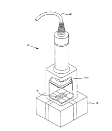
Fig. 1 is an isometric view with partial cut-away of an
apparatus according to the invention in use.
Figs. 2A and 2B are an exploded isometric view of an
apparatus according to the invention.
Fig. 3 is a plan view of an LED array according to the
invention.
Fig. 4 is a basic circuit diagram for the LED array
according to the invention.
Detailed Descri~tion of a Preferred Embodiment.
Referring to Figure 1, there is shown a fully-assembled
illumination and imaging apparatus lO according to the invention
in use, in partial cut-away. Apparatus 10 is shown in use in
~ WO 94/19764 PCTrUS94/01661
211 ~15~
obtaining an image of label 14 affixed to a surface of package
12. Apparatus 10 is positioned 80 as to completely cover label
14. Apparatus 10 has illumination assembly 100. Diffuse light
generated by illumination assembly 100 uniformly illuminates
label 14 while label 14 is imaged by CCD camera assembly 200 (not
shown in Figure 1) disposed inside apparatus 10. An electronic
sisnal representing the image of label 14 obtained by CCD camera
assembly 200 (not shown in Figure 1) is then transmitted from
apparatus 10 to a data processing unit (not shown) external to
apparatus 10 through cable 16.
Referring now to Figures 2A and 2B, apparatus 10
includes illumination assembly 100, CCD camera assembly 200,
shroud 300, and handle assembly 400. Illumination assembly 100
includes LED mounting board 110 and LED trigger board 180. Both
LED mounting board 110 and LED trigger board 180 are substantial-
ly planar and square in shape, with central circular holes 112
and 182, respectively, disposed therethrough.
LED mounting board 110 serves as the mounting base for
the two-dimensional array of LEDs 120. Referring now to
Figure 3, LEDs 120 are arranged on LED mounting board 110 in a
large number of parallel horizontal rows, with equal spacing of
LEDs 120 within each row, and the rows equally spaced from one
another. Each horizontal row of LEDs 120 is offset by half the
center-to-center spacing of the LEDs 120 in the preceding and
WO 94/19764 PCTrUS94/01661 ~
2~ 5 2
succeeding horizontal rows. LEDs 120 are mounted on LED mounting
board 110 by conventional mounting means.
LEDs 120.may be electrically connected in the circuit
depicted in Figure 4. Two individual LEDs 120 are connected in
series to form a single LED string. Individual LED strings are
then connected to each other in parallel, with a current limiting
resistor in the circuit between the LED strings and the power
source. By way of example only, this embodiment has eighty-nine
LED strings connected in parallel constituting the full two-
~im~n~ional LED array covering LED mounting board 110. Power is
provided to LEDs 120 on LED mounting board 110 by LED trigger
board 180. The large number of LEDs, here 178, and their gener-
ally equal spacing across LED mounting board 110, provides
uniform illumination. The number of LEDs may of course be
increased, to the extent permitted by space limitations. The
number of LEDs may also be reduced. However, as the number of
LEDs is reduced, uniformity of illumination is reduced.
Referring to Figure 2B, LED trigger board 180 contains
the control and power circuitry for LEDs 120 mounted on LED
mounting board 110. LED trigger board 180 receives power from
either an external source (not shown) via cable 16 or an internal
power source (not shown). As depicted on Figure 4, energy may be
stored in one or more capacitors 194 mounted on LED trigger board
180. When apparatus 10 is not being used to obtain images of a
WO 94/19764 2 1 5 ~ 1 ~ 2 PCTrUS94/01661
surface, field effect transi5tor 192 allows power to flow only
from the external or internal power source (not ~hown) directly
to capacitors 194, allowing capacitors 194 to charge. When a
imaging activation signal is received by controller 190, control-
ler 190 sends a signal to field effect transistor 192 to open the
circuit between capacitors 194 and LEDs 120. Capacitors 194 thus
discharge stored electrical energy through current limiting
resistor 196 into LEDs 120 mounted on LED mounting board 110,
causing LEDs 120 to flash. At the same time, a data processing
unit (not shown) external to apparatus 10 causes CCD camera
assembly 200 to obtain an image of the now illuminated target
surface.
By way of example only, a working embodiment of illumi-
nation assembly 100 will be described in detail. LED mounting
board 110 is a square circuit board approximately 2.75 inches by
2.75 inches. LED mounting board 110 has a central circular hole
112 1.54 inches in diameter disposed therethrough, the center
being an equidistant 1.375 ;nch~s from the outside edges of LED
mounting board 110. In each corner, LED mounting board 110 has a
hole 114 0.125 inches in diameter disposed therethrough for
purposes of attaching LED mounting board 110 to LED trigger board
180 using small standoffs 186 and screws 118. The center of each
hole 114 is approximately 0.125 inches from the outside edges of
LED mounting board 110.
WO 94/19764 PCTrUS94/01661
2~5~2
Each LED is a Hewlett-Packard HLMP-K105 "Red" LED lamp.
These LEDs were selected for their excellent energy efficiency.
As described above, LEDs 120 are electrically connected into 89
LED strings in parallel, each LED string defined by 2 LEDs 120 in
series. LEDs 120 are arranged on the surface of LED mounting
board 110 in 24 parallel horizontal rows, with equal spacing of
LEDs 120 within each row, and the rows equally spaced from one
another. Each horizontal row of LEDs 120s is offset by half the
center-to-center spacing of the LEDs 120 in the preceding and
succeeding horizontal rows. In a single horizontal row, individ-
ual LEDs 120 in that row are separated by 0.2 inches, as measured
from the center of one LED 120 to the center of the next LED 120.
Each horizontal row of LEDs 120 is separated from the preceding
or succeeding horizontal row of LEDs 120 by 0.1 inches, as
measured from the center of LEDs 120 in that horizontal row to
the center of LEDs 120 in the preceding or succeeding horizontal
rows. In the imaging sequence, capacitors 194 provide 7.0 amps
of current at 6 volts for one millisecond. As a result, LEDs 120
consume only 0.042 joules of energy per flash while generating
enough light to uniformly illuminate the target surface. This
low power consumption allows apparatus 10 to operate with an
internal power source, such as a rechargeable battery pack,
making apparatus 10 a truly portable unit.
LED trigger board 180 is also a square circuit board
approximately 2.75 inches by 2.75 inches. LED trigger board 180
WO 94/19764 2 1 5 G 1~ ~ PCTrUS94/01661
has a central circular hole 182 1.54 inches in diameter disposed
therethrough, the center being an e~uidistant 1.375 inches from
the outside edges of LED trigger board 180. In each corner, LED
trigger board 180 has a hole 184 0.125 inches in diameter
disposed therethrough for purposes of accommodating screws 118 to
attach LED trigger board 180 to LED mounting board 110 using
small standoffs 186, and to attach LED trigger board 180 to
mounting board 230 using screws 118 and large standoffs 232. The
center of each hole 184 is approximately 0.125 inches from the
outside edges of LED trigger board 180. Capacitors 194, field
effect transistor 192 and current limiting resistor 196 are
mounted on LED trigger board 180. Capacitors 194 are 2 Nichicon
4700 uf capacitors, part number URSlA472MRA. These capacitors
were selected for their large storage capacity and small physical
size. By way of example only, current limiting resistor 196 may
be a single 0.25 ohm resistor, or may be a string of four 1 ohm
resistors connected in parallel.
Referring again to Figure 2B, CCD camera assembly 200
is the means by which apparatus 10 obtains images of the illumi-
nated target surface. CCD camera assembly 200 includes CCD
camera 210, camera lens 220 and mounting board 230. CCD camera
210 contains the CCD imaging elements (not shown) and is connect-
ed to a data processing unit (not shown) external to apparatus 10
via cable 16. Camera lens 220 focuses the surface to be imaged
WO 94/19764 PCT~US94/01661
2 ~ 2
on the CCD imaglng elements (not shown) disposed inside CCD
camera 210.
~ m-n~ion assembly 100 and CCD camera assembly 200
are assembled together for insertion and mounting in shroud 300.
CCD camera 210 and camera lens 220 are disposed through central
circular hole 234 in mounting board 230, with camera lens 220
extending downward from mounting board 230 through central
circular holes 112 and 182 in LED mounting board 110 and LED
trigger board 180 so that a clear view of the target surface is
obtained. CCD camera 210 and camera lens 220 are attached to
mounting board 230 by attachment ring 236. Once CCD camera 210
and camera lens 220 are attached to mounting board 230 and camera
lens 220 is disposed through central circular holes 112 and 182
in LED mounting board 110 and LED trigger board 180, screws 118
are disposed through holes 114 in LED mounting board 110, through
small standoffs 186, through holes 184 in LED trigger board 180
and into large standoffs 232 attached to mounting board 230.
When screws 118 are tightened, illumination assembly 100 compo-
nents are rigidly attached to CCD camera assembly 200, thus
forming one single unit for insertion and mounting in shroud 300.
Because camera lens 220 is mounted inside apparatus 10
at a fixed distance from the lower edge of shroud 300, and hence
a fixed distance above the target surface, no adjustments are re-
quired to obtain a clear image of the target surface during the
--10--
WO 94/19764 21~ 2 PCT~US94/01661
imaging process. Proper focusing of CCD camera 210 is achieved
by simply placing apparatus l0 on the surface to be imaged. By
way of example only, the CCD-based camera may be a Pulnix TM-7X
camera with a TAMRON 6.5 mm lens.
In an alternative embodiment, a narrow bandpass filter
and/or a polarizer/analyzer may be employed to enhance the
clarity of the image obtained from the target surface. In this
alternative embodiment, the bandpass filter or ~he analyzer may
be a cap type assembly which fits securely over camera lens 220,
or may be fabricated in such a way as to integrally connect with
camera lens 220. The polarizer would typically be a thin film
disposed downward of LED mounting board ll0, with a hole there-
through for camera lens 220. The b~n~p~s ~ilter or analyzer
would be disposed between camera lens 220 and the target surface,
so that light reflected back from the target surface passes
through the bandpass filter or analyzer before reaching camera
lens 220.
The narrow bandpass filter allows only light in a
selected region of the spectrum in which the LEDs emit to reach
the CCD imaging elements, thereby eliminating the image distort-
ing effects of radiated light in the infrared region of the
spectrum and of ambient illumination. By polarizing light
transmitted to the target surface in a first direction, and
polarizing light reflected back from the target surface in a
WO 94/19764 PCTrUS94/01661 ~
21~6~2
second direction, the polarizer/analyzer eliminates substantially
all glare caused by specular light reflecting off the target
surface. This virtually eliminates any glare induced "hot spots"
on the image obtained by CCD camera assembly 200.
Shroud 300 has a generally vertical opaque sidewall,
and may be square in section. The top 310 of shroud 300 is com-
pletely open to receive the assembled components of illumination
assembly 100 and CCD camera assembly 200. Mounting board 230 of
CCD camera assembly 200, with attached illumination assembly 100,
fits snugly inside the opening in top 310 of shroud 300 and is
attached to shroud 300 using conventional mounting means. Shroud
300 also has an open base 320 to allow shroud 300 to completely
cover a surface to be imaged, blocking out substantially all
sources of light external to apparatus 10 while allowing light
radiating from illumination assembly 100 to uniformly illuminate
the surface to be imaged.
Shroud 300 is made of an opaque material, such as
molded plastic. The internal surfaces of shroud 300 below
illumination assembly 100 may be coated with a light-reflective
material, such as a thin al-lm;nl-m film. This coating will
~nh~e the illumination intensity and increase the illumination
uniformity on the surface to be imaged. Preferably, the entire
internal surface, or substantially the entire internal surface of
shroud 300 below illumination assembly 100 is light reflective.
-12-
~ WO 94119764 PCTrUS94/01661
2156152
Handle assembly 400 includes main handle 410, strain
relief 420, and swltch 430. Main handle 410 ~erves as a conduit
for cable 16, an enclosure for CCD camera 210, and a handgrip for
apparatus lO. Main handle 410 is a hollow, rigid metal tube with
a foam rubber grip surro~n~; ng its outer circumference. The foam
rubber grip allows for easy handling of apparatus lO during
operation. CCD camera 210 is disposed inside main handle 410,
and cable 16 is routed through central circular opening 432 in
switch 430 and is disposed inside main handle 410, attaching to
the top of CCD camera 210.
A circular mounting ring 412 defines the bottom portion
of main handle 410. Handle assembly 400 attaches to CCD camera
assembly 200 by disposing screws through holes 414 in mounting
ring 412 and into holes (not shown) in the upper side of mounting
board 230.
Strain relief 420 defines the top of handle assembly
400. Strain relief 420 is preferably made of flexible plastic
molded in a helical "pigtail" shape 422 which is disposed around
cable 16. Cable 16 is routed through hole 424 in the top of
strain relief 420. The bottom lip 426 of strain relief 420 is
preferably made of rigid plastic and fits snugly inside the
central circular opening 432 in switch 430. In operation, strain
relief 420 flexes back and forth restricting the lateral movement
WO 94/19764 PCTrUS94/01661 ~
2, l ~i ~; 15 S2
of cable 16, permitting the operator to move apparatus 10 without
damaging or severing cable 16.
Switch 4.30 is mounted on the top of main handle 410 by
conventional mounting means. Switch 430 may be a conventional
omnidirectional switch. Switch 430 wiring is routed internally
to controller 190. A central circular hole 432 is defined in the
top of switch 430 to accommodate bottom lip 426 of strain relief
420 and to internally route cable 16.
Referring to Figure 4, during operation of apparatus
10, switch 430 serves as the means for activating the illumina-
tion and imaging sequence of apparatus 10. When switch 430 is
activated, an activation signal from switch 430 is sent to
controller 190. Once the activation signal is received, control-
ler 190 sends a signal to field effect transistor 192 to permit
current to flow from capacitors 194 to LEDs 120 causing LEDs 120
to flash, while simultaneously a data processing unit external to
apparatus 10 triggers CCD camera assembly 200 to take an image of
the illuminated target surface.
In operation, an operator positions apparatus 10 over
the surface to be imaged so that shroud 300 covers as much of the
surface as possible. To begin the imaging sequence, the operator
activates switch 430. Switch 430 sends an activation signal to
controller 190. The activation signal starts a 1 millisecond
timing circuit in controller 190. At the same moment the timing
~ WO 94tl9764 21~ ~15 2 PCTrUS94/01661
circuit is activated, controller 190 sends a signal to field
effect transistor 192 to open the flow of power from capacitors
194 to LEDs 120 mounted on LED mounting board 110. Capacitors
194 discharge through current limiting resistor 196 into LEDs
120, causing LEDs 120 to flash. A data processing unit external
to apparatus 10 also receives the activation signal via cable 16
and signals CCD camera assembly 200 to obtain an image of the now
illuminated target surface. CCD camera assembly 200 takes the
image, which is transferred back to the external data processing
unit via cable 16. The entire imaging sequence is completed
before the 1 millisecond timing circuit in controller 190 ex-
pires. Once the timing circuit expires, controller 190 sends a
second signal to field effect transistor 192 to shut off the flow
of power from capacitors 194 to LEDs 120, reestablishing the flow
of power from the external or internal power source to capacitors
194, allowing capacitors 194 to recharge for the next imaging
sequence.
By using a two-~im~n~ional array of LEDs affixed to a
surface, the present invention permits diffuse illumination
radiating from the LEDs to reach a surface to be imaged without
"hot spots" or "shadows," creating uniform illumination across
the entire surface. This allows the imaging apparatus to obtain
a complete and accurate image of the surface for further data
processing. The LEDs may be selected for extreme energy effi-
ciency, resulting in low power consumption with no degradation in
WO 94/19764 PCTnUS94/01661
21~6152
illumination. The device can accordingly be operated using only
a rechargeable battery pack, making the device a truly portable
unit.
It will be appreciated that there are considerable
~ariations that can be accomplished in a method and apparatus of
the invention without departing from its scope. As a result,
although a preferred embodiment of an apparatus of the invention
has been described above, it is emphasized that the invention is
not limited to a preferred embodiment and there exist other
alternative embodiments that are fully encompassed within the
invention's scope, which is limited only by the scope of the
appended claims.