Note: Descriptions are shown in the official language in which they were submitted.
WO 94/19051 PCT/US94/01721
A SPATIALLY DISTRIBUTED SMA ACTUATOR FILM
Background
The field of the present invention relates
generally to shape memory alloy (SMA) actuators.
More particularly, the field of the present
invention relates to a spatially distributed
actuator film wherein a plurality of SMA actuator
elements together with associated control and driver
circuitry are deposited on a thin, flexible
substrate using very large scale integrated circuit
(VLSI) techniques.
The basis for a conventional steerable element
such as a steerable catheter incorporating a shape
memory alloy actuator is the ability of certain ~_
t
special alloys to undergo a micro-structural
transformation from an austenitic phase at high
temperature to a flexible, so-called martensitic
phase at a lower temperature. One of the more
common and useful alloys is a 49:51 composition of
titanium and nickel (TiNi). The temperature at
which the phase transition occurs is referred to as
the activation temperature. For the foregoing
composition, this is approximately 70°C. In the low
temperature region, the SMA actuator is soft and
' exhibits a Young's modulus of 3,000 MPa. In this
state, the shape memory alloy may be readily
deformed up to 5% in any direction without adversely
affecting its memory properties.
WO 94/19051 PCT/US94/01721
- 2 -
Once heated just beyond the activation .
temperature, a phase transformation from the soft,
pliable martensite to harder, inflexible (6900 Mpa)
austenite, the parent phase, takes place. That is,
if the shape memory alloy material is ano:~Y
excessively deformed or is not over-cstrained, it
attempts to reorganize its structure.-to a previously
"memorized" shape. If permitted to cool, the shape
memory alloy becomes soft again and may be
mechanically deformed to begin another cycle. The
mechanical deflections produced by activating the
memorized state can produce useful work if suitably
configured. Although the recovery deflections may
be small (5%), the recovery forces can range from in
the neighborhood of 35 tons per square inch or more
for linear contractions. Thus, the recoverable
energy is considerable.
Any shape may be programmed into an SMA
actuator element by physically constraining the
piece while heating it to the proper annealing
temperature. TiNi alloys are commercially available
in sheet, tube and wire forms and can have a wide
range of transformation temperatures.
A memory transformation of an SMA element is
dependent upon temperature. However, the rate of
deformation is dependent on the rate of cooling and
heating. Therefore, the rate at which temperature
changes take place dictates the maximum speed at
which the SMA actuator can operate. As with all
mechanical designs, there is a tradeoff. A faster
WO 94/19051 - ~ ~ 5 ~ 4 31 ., PCT/US94/01721
- 3 -
actuating SMA actuator must be heated and cooled
faster, thereby consuming more power and generating
a larger amount of wasted heat.
It is 7triown to use shape memory alloy actuators
in conventionally steerable elements such as
catheters. One such application, U.S. patent
no. 4,543,090, describes a conventional steerable
and aimable catheter using shape memory alloy as the
control elements. Conventional steerable devices
using SMA elements are severely limited in
dexterity. Movement is limited to a single plane.
Also, the SMA element must be mechanically deformed
to begin another cycle.
Thus, in conventional applications, each shape
memory element must be coupled to at least one other
shape memory element. When one of the elements is
heated, it is returned to its original position by
the other memory element. This enables controlled
motion, however only in a plane. The motion is
limited to at most, two degrees of freedom per
j oint .
Conventional steerable devices such as
catheters incorporating SMA actuators as control
elements have considerable disadvantages. The
joints must be made unduly large and cumbersome
because an opposite force is always needed to return
the SMA actuator element to its martensitic shape
after transformation from the parent phase. Complex
linkages are required in order to rotate such a
., r
WO 94/19051 : a PCT/US94/01721
- 4 -
steerable device. For example, the range of .
maneuverability is severely limited by the linkages
which are necessary to return the SMA actuator .
element to its martensitic shape a.~,t~~r it has been
activated to assume its programmed'~=shape.
Conventional steerable devices using shape
memory alloys have a further disadvantage in that
they are relatively large and have a severely
constrained lower limit beyond which size reduction
is not economically feasible. The relatively large
size is due to the need for control arms, linkages
or other elements which are necessary to return the
shape memory actuator to its initial state. This
severely constrains the geometry of such a
conventional steerable device.
Conventional steerable devices incorporating
shape memory alloys lack the dexterity and precise
control necessary to maneuver into very small,
geometrically complex spaces. This is due to the
need for control arms or oppositely disposed
elements for mechanically returning the actuator to
a first position after it has been activated to its
programmed state.
Conventional steerable devices using SMA
actuators are often too slow for many medical
applications where quick, dexterous movement is
critical. The large size of conventional steerable
devices using SMA elements requires an increased
amount of current in order to produce the activation
WO 94/19051 _ 215 6 4 31 PCT~S94/01721
- 5 -
temperature needed for a quick transition from the
martensitic state to the programmed or "memorized"
austenitic phase. A conventional SMA actuator
consumes a great deal of power, thus dissipating a
h
large amount of heat. This necessarily slows down
the cooling to the activation threshold and thereby
slows down the transition from the austenitic state
back to the martensitic state, resulting in a slower
acting device.
What is needed is a steerable device which is
capable of unrestricted yet highly precise and
dexterous maneuvers in three- dimensional space. It
would be advantageous to eliminate the need for
control arms, linkages, or other extraneous means
for returning conventional shape memory alloy
elements to a first position after deactivation and
the transition from the parent phase back to the
martensitic state. Such control linkages increase
the size of the device, increase power requirements
and. slow the dissipation of heat, resulting in a
slow acting device.
What is also needed is a steerable device
capable of unrestricted articulation in three
dimensions, and which can be scalable for providing
increased dexterity and maneuverability in very
small, geometrically constrained areas which are
presently inaccessible to conventional steerable
devices.
WO 94/19051 PCTlUS94/01721
..
- 6 -
r ,
SUMMARY
In order to overcome the above-discussed .
disadvantages of conventional steerable devices
using shape memory alloy actuators, one aspect of
the present invention utilizes the fact that SMA
alloys can be deposited, patterned and annealed
using conventional VLSI techniques. The broad range
of fully developed VLSI tools and techniques greatly
reduce the cost of fabrication and assembly of small
steerable devices such as catheters. To fabricate a
steerable device in accordance with the present
invention such as a 6F (French) catheter, the SMA
thin film actuators are deposited by conventional
chemical vapor deposition (CVD), and VLSI
techniques, and patterned on a thin, flexible
silicon nitride or polyimide film. Electrical
connections are made using standard photolitho-
graphic processes. After releasing the SMA actuator
"skin" or film from its silicon processing base, it
is adapted to be wrapped around any flexible surface
to impart torque thereto, such as a force glove, or
to impart three dimensional movement. In one
embodiment, the SMA actuator film is adapted to be
wrapped in a cylindrical configuration around a
bendable element such as a flexible catheter tube,
or the like. The SMA actuator elements are thereby
spatially distributed around the circumference of
the bendable element. The SMA actuator elements are
then controllably selected to move the bendable
element any direction in three-dimensional space.
WO 94/19051 PCTIUS94/01721
The VLSI fabrication of the thin film SMA
actuator elements in accordance with one aspect of
the present invention achieves a more rapid
dissipation of heat than is possible with
conventional SMA devices. This results in a faster
acting device. It also has the advantage that a
steerable catheter sheathed with the SMA actuator
film of the present invention can be articulated at
100 Hz. A catheter having a dimension of 6 French,
encased by the SMA actuator film of the present
invention, can be articulated at ~ second intervals.
In accordance with another aspect of the
invention, a plurality of on-off switch means are
integrally formed using VLSI techniques on the same
flexible substrate which also forms the SMA actuator
film. The switch means are disposed for providing a
phase activation threshold current to selected SMA
actuators to produce the phase transition from
martensite to austenite and thereby impart desired
movement. In a preferred embodiment, the switch
means comprise a plurality of a CMOS power
transistors. The transistors and associated address
decode circuitry are operatively linked with a
corresponding one of each of the SMA actuators for
selectively applying a phase activation current
thereto. VLSI fabrication eliminates the need for a
multitude of current carrying wires to the SMA
actuators. Only three leads, a ground lead, power
lead, and data signal lead are necessary for linking
address decode and circuitry with an external
WO 94/19051 PCT/US94/01721
_8_
microprocessor. Alternatively, control data may be
modulated along a single power lead.
~s
f
'a~
A microprocessor controller is wised for
programming a predetermined path.o~f~travel for the
SMA actuator film. The microprocessor is a
separately packaged integrated circuit which
communicates with the control circuitry on the SMA
actuator film through conventional leads, or fiber
optic links.
In accordance with another aspect of the
present invention, the microprocessor includes a
position mapping means. Pressure sensor means are
disposed along the distal or active end of the SMA
actuator film. The pressure sensor means provide
output signals at precise positional intervals to
the microprocessor. The output signals are
representative of pressure sensed when the distal
end or exterior skin of the SMA actuator film is
pushed against a boundary defining a travel path
such as the wall of an artery. The microprocessor,
in accordance with well known adaptive feedback
techniques, uses the output signals from the sensory
means to determine a locus of angular positions for
the SMA actuators which define an ideal path of
travel as the SMA actuator film is advanced into a
geometrically complex space. The position mapping
means records the angular positions of the SMA
actuators for precise positional intervals along the
path of travel as the steerable device is advanced
into a geometrically complex space. Upon
WO 94/19051 PCT/US94101721
- 9 -
. retraction, the position mapping mans produces
output signals to the control circuitry for
activating the SMA actuators in a reverse sequence
along the path~of travel. The configuration of the
SMA actuator film is thereby automatically recreated
for each of the positional intervals along its path
of travel in a reverse direction. This enables the
SMA actuator film of the present invention to
maneuver dexterously in a reverse direction in
geometrically complex spaces which are inaccessible
to conventional steerable devices using SMA actuator
elements.
In accordance with an aspect of the invention,
the position of the distal or active end of the SMA
actuator film can be inferred by measuring the
resistance of the SMA actuator elements using
conventional techniques which are well known to one
skilled in the art. The resistance of each element
is proportional to its temperature, thus to its
activation state and to its angular position.
Accordingly, the overall configuration of the SMA
actuator film can be determined by the
microprocessor for any given point in a locus of
points which define a path of travel.
It will be appreciated that in accordance with
another aspect of the invention, the SMA actuator
film is self-guiding with respect to a locus of
points defining an ideal path of travel, once the
angular positions of the SMA actuator elements for
WO 94/19051 ~~~ ~ ~~ PCT/US94/01721
H
- 10 -
each of those points have been stored in the ,
position mapping means.
,
In accordance with another aspect of the
invention, the reduced cost of:the SMA actuator
film made possible by VLSI fabrication enables the
SMA actuator film to be detachable and disposable
after use. The SMA actuator film which encases a
catheter, for example, and enters an artery, is
connected to external control circuitry over
flexible leads through a simple plug/socket
connector. The SMA actuator film is thereby
detachable from control circuitry, and easily can be
replaced after use.
The fabrication of the spatially distributed
SMA actuators, associated address decode circuitry
and power transistors using thin film VLSI
techniques enables a steerable device in accordance
with the present invention, to be capable of being
scaled down in size to much less than 6F (French)
which is equal to 1900 microns. This has many
advantages over conventional steerable devices using
SMA memory elements, including smaller size, greater
maneuverability, lower power consumption, more rapid
heat dissipation, and consequently, faster movement.
The scaled down size achievable by the present
invention also enables a device to dexterously
maneuver through geometrically complex spaces in
three dimensions which are inaccessible to
conventional devices.
WO 94/19051 ~ PCT/US94101721
- 11 -
Brief Descrivtion of the Drawings
These and other advantages of the present
invention may be appreciated from studying the
following detailed description of the invention
together with the drawings in which:
FIGURE 1A is a top view of a first embodiment
according to the present invention;
FIGURE 1B is a perspective view of the
embodiment depicted in FIGURE 1A;
FIGURE 1C is an enlarged perspective view of
the embodiment depicted in FIGURE 1A;
FIGURE 2A is a side sectional view of the
embodiment depicted in FIGURE 1A;
FIGURE 2B is a sectional end view of an
alternate embodiment of the invention shown in
FIGURE 1A;
FIGURE 3A is a cut-away perspective view of the
embodiment depicted in FIGURE 1 showing how the
spatially distributed SMA actuator film of FIGURE 1
is adopted to be wrapped around and secured to a
flexible, bendable structure;
FIGURE 3B is a side sectional view of the
embodiment depicted in FIGURE 3A;
WO 94/19051 ~ PCT/US94/01721
- 12 -
FIGURE 4 is a perspective, sectional view of
.,
the embodiment depicted in FIGURES 31~=~and 3B,
showing the phase activation action~,bf an SMA
element; and
FIGURE 5 is an equivalent circuit diagram of
the embodiment depicted in FIGURE 1.
FIGURE 6 is a perspective view of an embodiment
according to the present invention showing an
example of distributed articulation in three-
dimensional space.
FIGURE 7 is a schematic diagram of a typical
pressure sensor means for adaptive feedback control
of the embodiment shown in FIGURE 6.
FIGURE 8 is a perspective view of an apparatus
for measuring the angular displacement of the SMA
actuator elements to provide precise control of the
SMA actuator film.
DESCRIPTION
Overview
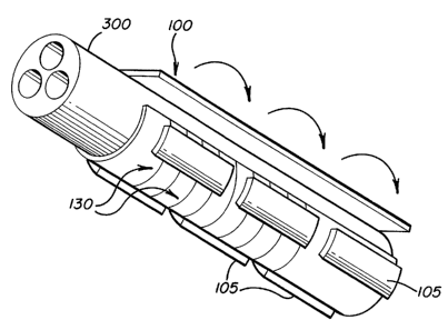
As shown in FIGURES 1A, 1B and 1C, a spatially
distributed SMA actuator film 100 comprises a
plurality of SMA thin film actuators 105 disposed in
a distal portion thereof. The SMA actuators 105 are
deposited, patterned and annealed on a layer of
polyimide or kevlar based material using
conventional VLSI techniques.
WO 94!19051 _ 2~~~~ 6 4 3 I PCT/US94/01721
- 13 -
.Electrical connections with address decode
circuitry 118 and associated switch means 114 such
as CMOS transistors are made using standard VLSI
photolithographic processes.
The layer 108 of polyimide or kevlar based ,
material is released from a silicon processing base
using standard techniques such as EDH etch, or the
like. This subsequently forms a self-contained,
flexible SMA actuator film 100 wherein the SMA
actuators 105, as well as associated switch means
114 for applying the phase activation current to
selected SMA actuators 105, and address decode
circuitry 118 are integrated in VLSI on a compact,
flexible SMA film 100.
The SMA actuator film 100 is adapted to be
wrapped around any surface configuration to impart
torque thereto, such as a force glove or the like.
In a preferred embodiment, the SMA actuator film 100
is adapted to be wrapped around a bendable element
such as a catheter tube 300, or the like as shown in
FIGURES 3A and 3B. Accordingly, a plurality of SMA
actuators 105 are then evenly distributed around the
surface of the SMA actuator film 100 which encases
the bendable element 150. Selective activation of
the SMA actuators 105 by the control circuitry
thereby imparts continuous movement in any direction
in three dimensional space to the bendable element.
In the example shown in FIGURE 3B, three thin
film SMA actuators 105 are positioned at 120°
WO 94/19051 ~ ~ !~ PCT/US94/01721
14
intervals around a flexible catheter '~u~e 300. With
reference to FIGURE l, the SMA act ~~ors 105 are
selectively addressed by address decode circuitry
118 and are resistively heated by transistor switch
means 114 to a phase activation threshold in
accordance with techniques which are well known.
Selectively applying a current to one or more of the
SMA actuators 105 which is sufficient to activate
the shape memory phase transition produces a
differential contraction on one side of the tube
300, and local bending. ,
The SMA actuators 105 are deactivated by
removing the current source thereby permitting heat
to flow from the SMA actuator 105. The rate at
which the SMA actuators cool is determined by their
thickness. It will be appreciated that the
spatially distributed SMA actuators 105 form a
multijointed manipulator or multi-segmented probe
which is not constrained to move in a single plane
but can bend in any direction with unrestricted
motion.
It also will be appreciated that the
integration of the SMA actuators 105 in overlapping
arrays in a flexible VLSI film produces a continuity
of moveable SMA nodes which are spatially
distributed around the circumference of a bendable
element. This enables a bendable element encased by
the SMA actuator film 100 of the present invention .
to be capable of substantially continuous movement
in three dimensions along its length. Thus, the SMA
WO 94/19051 . I ,. PCTlUS94/01721
- 15 -
actuator film 100, when wrapped around a catheter
tube or the..~ike, is able to execute extremely
dexterous maneuvers in three-dimensional space.
This was not possible with conventional steerable
devices using shape memory alloy actuators which are
constrained to move in a single plane.
Process for Making the SMA Actuator Film
Referring now to FIGURES 1C and 2A, in
accordance with one aspect of the invention, the
overall process for forming the spatially
distributed SMA actuator film is as follows.
A substrate 200 is initially provided as a
foundation for VLSI integration of control and
address circuitry and SMA actuator elements. A
standard silicon wafer, [100]Si, having a thickness
of approximately 500 microns is a suitable base
substrate material.
Next, a series of grooves are formed in the
silicon wafer using an anisotropic etch. The
grooves provide a corrugated foundation in substrate
200 which will be used to form a series of
corrugations 130 in a subsequently deposited
polyimide layer 108 which will be used to form the
VLSI SMA actuator film 100.
The corrugations 130 are located substantially
beneath each SMA actuator element 105. The corruga-
tions are disposed substantially transversely to the
axes of deformation or actuation axis of the SMA
WO 94/19051 PCT/US94/01721
~1~s4~~ _ . .. ~. ,
- 16 -
actuator elements 105. The corrugations 130 provide .
a means for enabling the actuator elements 105 to
f,, ..
deform upon actuation and to impart~~rriovement to an ,
entire adjacent portion of SMA ac~~,iator film 100.
The corrugations 130 thus facilitate the controlled
movement of the SMA actuator film 100 upon
application of an electric current. The size and
configuration of the corrugations 130 can be scaled
to maximize the movement induced in the SMA actuator
film 100 by the contraction or expansion of actuator
elements 105.
The corrugations 130 also provide a means for
limiting strain in the actuator elements and in the
SMA actuator film 100 and thus prevent breakage of
the SMA actuator film 100. In a preferred
embodiment, the corrugations 130 limit the strain to
approximately s8%.
After the forming the corrugations 130, a thin
insulating layer 109 of SiNi is deposited over the
wafer 200 using conventional VLSI techniques which
are well-known. The layer 109 of SiNi acts as an
oxygen barrier to prevent contamination of the TiNi
layer which is to be sputtered in a subsequent
process step. The layer 109 of SiNi has a thickness
which is on the order of 2000A.
The shape memory alloy material such as a 50:50
or 49:51 TiNi formulation is then sputtered over the
layer 109 of SiNi in accordance with well-known
CVD/VLSI techniques. The TiNi is then annealed to
WO 94/19051 w ~ ~ ~ 6 4 3 ~. . 1 PCT~S94/01721
- 17 -
its programmed parent phase. The annealing process
is dependent upon the formulation of TiNi used. The
TiNi layer is typically annealed at 510°C-540°C for
one hour.
As will be explained, the TiNi layer 105 can be
annealed to optimize the useful torque to be
extracted from the transition to the parent phase.
The layer of TiNi is then patterned and etched
according to known VLSI techniques to form discrete
TiNi SMA actuators 105. The TiNi actuators 105 are
then masked.
A layer 108 of polyimide or other kevlar based
material is deposited over the TiNi actuators such
that windows are formed around each TiNi actuator.
The layer 108 of polyimide provides the foundation
for the VLSI fabrication of switch means 114,
address decode circuitry 118 and conductive paths
112 as shown in FIGURE 1B. The polyimide layer 108
can be as thin as one-half micron.
Polyimide has proved to be a high precision,
high strength mechanical material, which is
especially applicable in this case when SMA
actuators and associated control and driver
circuitry must be integrated in VLSI on a very thin
sheet which must exhibit great flexibility, yet be
high in strength.
While polyimide is preferred as a foundational
material, the VLSI SMA actuator film is not intended
WO 94/19051 PCT/LJS94/01721
~~~6~~~. .
- 18 -
to be limited to polyimide and any appropriate
flexible sheet material for accepting VLSI
processing techniques may be implemented without
departing from the scope of the~'~invention.
A plurality of switch means 114 such as CMOS
transistors suitable for VLSI fabrication are
provided over the polyimide layer 108. Each switch
means 114 is connected by conductive paths 112 to a
corresponding SMA actuator 105 for applying a high
current to that actuator to quickly resistively heat
the SMA actuator to its activation threshold. Each
switch means 114 is in turn connected with address
decode circuitry 118 which is also fabricated using
conventional VLSI techniques on the polyimide film
108. In a preferred embodiment address decode
circuitry 118 comprises a series of latch registers,
logic gates, or the like which are easily fabricated
in VLSI.
Conductive paths 112 between each of the TiNi
actuators and associated switch means and address
decode circuitry are also fabricated using
conventional VLSI techniques at this time.
As shown in FIGURE 2A, a conductive lead 112
makes electrical contact with one end of an SMA
actuator 105 through conductor termination block
201. A ground plane (not shown) is provided in the
polyimide layer 108 to provide a return current path
for the SMA actuators 105 in accordance with well
known techniques.
WO 94/19051 PCT/US94/01721
~~.5~6~.~~ ~,
- 19 -
VLSI sensor means such as capacitive linear
strain gauges, H~11 effect sensors, temperature
sensors, or the like. are likewise integrated in VLSI
on the polyimide layer 108 and are associated with a
corresponding SMA actuator or segment of SMA
actuator film 100 as will be explained.
The polyimide layer 108 is then released from
its silicon wafer processing base 200 by using a
conventional etching process such as an EDP etch.
It will be appreciated that the polyimide sheet now
comprises a fully integrated vLSI shape memory alloy
actuator film 100. That is, the SMA actuators 105,
address decode 118 and control circuitry, including
switch means 114, as well as positional sensors and
sensors for measuring environmental parameters, are
all integrally formed as a VLSI circuit incorporated
in a flexible polyimide sheet 100.
The fully integrated VLSI SMA actuator film 100
is detachably connected to a power source through
power lead 142. The SMA actuator elements are
connected to a common ground through ground lead
140.
A microprocessor (not shown) can be integrated
in VLSI on a proximal portion of the polyimide sheet
100 with address decode circuitry 118.
Alternatively, a microprocessor can be provided as a
separately packaged integrated circuit and
operatively connected with the address decode and
WO 94/19051 PCT/US94/01721
215 6 431
- 20 -
control circuitry on the polyimide sheet 100 through
data lead 142.
The foregoing process prov~d'es~ a self-
~r
contained, fully integrated VLS~.~'SMA actuator film
100 which can be operated in e.~ither open loop or
closed loop mode to provide unrestricted motion in
three dimensions as will be explained.
As shown in FIGURES 1A, 1B, and 1C in
accordance with another aspect of the invention, the
self contained VLSI SMA actuator film 100 may be
viewed as a module. The data signal lead 144, power
lead 142 and ground lead 140 are adapted to connect
together a plurality of cascaded VLSI SMA actuators
100 as modules. The VLSI SMA modules are combined
in sequential fashion. The data signal lead 144,
power lead 142 and ground lead 140 of a first VLSI
SMA actuator film module are carried forward to the
address decode circuitry 118 of each successive VLSI
SMA actuator module. Thus, a plurality of VLSI
shape memory actuator modules may be cascaded
together for certain applications.
The Shade Memory Actuators
In a preferred embodiment, the SMA material is
a 49:51 composition of titanium and nickel (TiNi).
The SMA material is available from RAYCHEM
Corporation, 300 Constitution Drive, Menlo Park,
California 94025. The SMA actuators 105 are highly
thermally sensitive elements which are resistively
heated to a phase activation threshold temperature
WO 94/19051 2 ~. 5 6 4 3 ~ ' PCT~S94101721
- 21 -
upon the application of a small electric current
through leads 112 as shown in FIGURE 1.
The formation of the SMA actuators is done
according to VLSI techniques which are well-known.
Typically, a suitable matrix of shape memory
material such as TiNi is vaporized using ion
bombardment in a low-pressure chamber. The
vaporized shape memory alloy atoms travel to a
substrate, in this case the silicon nitride base
layer 109, where the atoms condense in a film.
Referring to FIGURE 1, the shape memory actuator
film is patterned to form an array of SMA actuator
elements 105 by conventional VLSI photolithography
and etching operations to remove the sputtered SMA
material from areas where it is not desired. Thus,
a plurality of SMA actuator elements 105 are left on
top of the silicon nitride layer 109 as shown in
FIGURES 1 and 2.
The SMA actuator film is annealed at high
temperature in accordance with known techniques.
The annealing process programs the predetermined
shape into the SMA actuator elements which the
elements will assume after the microstructural
transformation from the martensitic phase to the
parent or austenitic phase. Any shape may be
programmed into the alloy by physically constraining
the piece while heating it to the proper annealing
temperature. For 49:51 TiNi, that temperature is
approximately 510°C for one hour. This is known as
the aging treatment.
WO 94/19051 PCT/US94/01721
~164~.
- 22 -
In a preferred embodiment, aR49:51 TiNi alloy _
is utilized for a one-way shape;:~einory actuator.
y
During the aging treatment,~the sputtered SMA film ,
.,, .,
is constrained in what is intended to be the high
,5 temperature shape. It will be appreciated that any
type of shape for maximizing the amount of movement
from the low temperature or martensitic phase to the
high temperature or austenitic phase may be
programmed. In the aging treatment, a precipitation
reaction in a TiNi alloy occurs. It is believed
that the precipitate particles effectively create a
back-stress which causes a deflection away from the
constrained shape (in the austenitic or programmed
phase) when the SMA actuator element is released and
cooled. Upon cooling, the TiNi alloy will
spontaneously deflect away from its constrained or
programmed shape.
It is known that the activation temperature for
the phase transformation from martensite to
austenite is alloy dependent and can be altered by
changing alloy composition. In accordance with
another aspect of the invention, this enables the
phase activation temperature to be optimized to
determine the minimum threshold current which is
necessary to achieve the spontaneous change of phase
to the programmed shape.
A phase transformation from martensite to the
parent phase or austenite is solely dependent on
temperature. However, the rate of deformation is
dependent on the rate of cooling and heating.
WO 94/19051 ~ 1 ~ 6 4 ~ ~ , pCTlUS94101721
,, '
- 23 -
Therefore, the rate at which temperature changes
takes place dictates the maximum speed at which a
SMA actuator can operate. As with all mechanical
designs there is a tradeoff. A faster actuating SMA
actuator must be heated and cooled faster, thereby
consuming more power and generating a larger amount
of waste heat.
As the SMA actuator elements 105 are
selectively resistively heated by the application of
an electric current, they generate controlled
movement of an adjacent portion of SMA actuator film
100. A 49:51 titanium nickel (TiNi) shape memory
alloy is the preferred material because this
exhibits a large change in shear modulus over a
relatively narrow temperature range. The change in
modulus at the activation temperature is the result
of a reversible martensite to austenite solid state
phase transformation.
One aspect of the present invention provides
significant power savings over conventional SMA
devices. The alloy mixture is optimized at 49:51
TiNi such that a minimum threshold current is
applied to the actuator elements 105 to achieve a
maximum amount of useful movement during the
transition from the martensitic phase to the
austenitic phase.
With regard to the configuration of the SMA
actuator elements, the TiNi or other suitable shape
memory alloy is sputtered so as form a matrix of
WO 94/19051 PCT/US94/01721
- 24 -
atoms which provide a pulling force by contracting '
when transformed to the high temperature austenitic
phase. This shape may be set by sputtering a matrix '
of suitable TiNi material in a compressed
configuration so that the SMA actuator element is
programmed upon annealing to be in a close,
compacted configuration. This is the so called
parent phase, the shape which is "remembered" at
elevated temperature. This is also termed the
austenitic phase. Thus, at a temperature below the
activation temperature, the TiNi elements can be
flexed outward and extended. Upon application of an
electric current, which resistively heats the SMA
actuator element to the phase activation
temperature, the SMA actuator element spontaneously
assumes its programmed configuration and contracts
the entire adjacent actuator film.
This is analogous to sputtering the SMA
actuator material in a configuration which may be
likened to a compression spring in its "remembered"
or programmed phase. Such a configuration would
spontaneously contract to provide a pulling force
when the SMA actuator element is resistively heated
to the phase activation temperature. Thus, such a
configuration would provide a pulling force when
activated. Whether the SMA actuator film of the
present invention operates in the compression or
tensile mode depends upon the mechanical constraints
which are imposed on the elements after annealing.
WO 94/19051 ' w, , PCTlUS94/01721
~~.~643~.
- 25 -
Various configurations of the SMA actuator
elements may be patterned by VLSI techniques to
optimize the pushing or pulling force which occurs
during the phase transformation from martensite to
austenite. In the preferred embodiment, the SMA
actuators contract upon being resistively heated to
the activation threshold.
In summary, the SMA actuator material is
deposited, patterned and annealed using conventional
VLSI techniques. The associated switch means 114
and address decode circuitry 118 are also deposited
in VLSI. on the polyimide layer. The polyimide layer
108 is released from its silicon processing base in
accordance with conventional etching techniques
which are well known. This provides a flexible,
modular SMA actuator film 100 wherein the SMA
actuators 105, associated control circuitry, such as
switch means 114 and address decode circuitry 118
are all integrated together in VLSI on the same
flexible substrate.
It will be appreciated that the flexible SMA
actuator film 100 may be configured around any
surface to impart movement or torque thereto. When
the SMA actuator film is wrapped around a central
longitudinal axis, the spatial distribution of the
SMA actuator elements 105 around the circumference
of the SMA actuator film 100 provides multi-node
articulation in three dimensions. A mufti-jointed
probe according to one aspect of the present
invention is capable of performing highly dexterous
WO 94/19051 PCTIUS94/01721
- 26 -
maneuvers in three-dimensior~,a~ space without
restriction.
One aspect of the invention overcomes a
significant problem with conventional SMA steerable
devices. This problem concerns the critical
restraints placed on the size and number of current
carrying conductors. Large TiNi actuators draw a
great deal of current requiring a corresponding
increase in the cross sectional area of the
conductors. This is not compatible with devices
having tight dimensional constraints. The foregoing
poses a critical problem which, until now, has not
been overcome. For example, some conventional TiNi
actuated catheters can only support a single
moveable joint due to this limitation.
To make a conventional SMA actuated steerable
catheter work with precision, it would be necessary
to deliver approximately 3 amps to the TiNi
actuator. The space constraints placed upon current
supplying feed wires are such that larger devices
draw a great deal of current if the TiNi actuators
are directly heated. The current supplying wires
would have to be prohibitively large and would
inhibit movement of the device.
Another problem with conventional SMA steerable
devices is that TiNi is difficult to control
accurately, since TiNi exhibits a temperature versus
resistance relationship with a significant
hysterisis curve.
WO 94/19051 ~ 15 6 4 31~ PCT~S94/01721
- 27 -
In order to overcome the foregoing
disadvantages of conventional SMA/TiNi actuated
devices, one aspect of the invention, as shown in
Figure 2B, provides a thin layer strain relief 202
of flexible, insulating material such as polyimide
which is deposited over each TiNi actuator 105. The
strain relief layer 202 has a thickness on the order
of 20,000A. Strain relief layer 202 can be thicker
or thinner, depending on the overall dimensions of
the SMA actuators. Subsequently, a very thin
conductive layer 204 is provided adjacent the stress
relief or insulating layer 202. The thin conductive
layer 204 comprises an ohmic heating means for
providing a high resistance heat source to the TiNi
actuator 105. The conductive layer 204 is also
termed an ohmic heating layer and preferably
comprises a thin layer of approximately 50:50 nickel
chromium (NiCr) .
The NiCr ohmic heating layer 204 provides a
higher resistance than bulk TiNi and ohmically heats
the TiNi element 105 to its phase activation
threshold by thermal conduction through insulating
layer 202. The TiNi element 105 is not electrically
connected to ohmic heating layer 204.
It has been found that the use of an ohmic
heating layer 204 in the present invention achieves
a considerable advantage over known SMA actuators in
that the supply current is greatly reduced, by at
least two orders of magnitude, for the same power
delivery. This is especially advantageous for
WO 94/19051 . . PCT/US94/01721
- 2g _
T.
devices of larger dime;_rislions, inhere supply current
1-
is critical. For example, in a large dimensional
SMA steerable device without the ohmic heating layer
204, the supply current would have to be increased
to an almost prohibitive degree in order to achieve
useful movement.
It has been found that an ohmic heating layer
204 comprising a metal such as NiCr does not exhibit
the resistance versus temperature hysterisis curve
of TiNi and is therefore capable of being controlled
with great accuracy. The ohmic heating layer 204
comprising NiCr is characterized by a linear
resistance versus temperature behavior, unlike TiNi,
thereby considerably reducing the controlling
effort.
In accordance with this aspect of the
invention, the linear temperature versus resistance
response of the ohmic heating layer 204 is used to
infer the temperature of an associated SMA actuator
105 and thus the degree of actuation and position of
the associated SMA actuator 105.
A predetermined current is passed through the
ohmic heating layer 204. Circuit means are provided
in accordance with known VLSI techniques for
measuring the drop in potential across the
electrical connections for ohmic heating layer 204.
This thereby enables the resistance of the ohmic
heating layer 204 to be determined.
WO 94/19051 ~ ~ 15 ~ 4 3 ~. PCT/US94/01721
- 29 -
Since the ohmic heating layer 204 is
characterized by a linear resistance versus
temperature response, the temperature of the ohmic
heating layer 204 is readily determined from the
known resistance. The temperature of ohmic heating
layer 204 is substantially equal to that of the
associated SMA/TiNi element. Thus, the temperature
indicates the degree of actuation or activation
state of the associated SMA actuator 105, and
consequently the position of the associated SMA
actuator. From this, the SMA actuators can be
precisely controlled in accordance with conventional
techniques which. are well known.
Referring now to FIGURES 3A and 3B, in
accordance with one aspect of the invention, the
flexible substrate comprising the SMA actuator film
100 is adapted to be configured around a central
longitudinal axis to provide unrestricted motion in
three dimensions. The SMA actuator film 100 is
wrapped around a bendable element such as hollow,
flexible catheter tube 300 or the like. It will be
appreciated that the corrugations 130 allow maximum
movement of the SMA actuator elements 105 and
consequently maximize the bending of the
cylindrically configured SMA actuator film 100 in
any direction in three-dimensional space. The
interleaved arrays of SMA actuator elements 105,
when wrapped around the circumference of bendable
element 300, as shown in FIGURE 3B, facilitate
unrestricted movement of the SMA actuator film 100
in three-dimensional space. As set forth
WO 94/19051 PCT/US94/01721
30 _ ~.y'.
..,
previously, the corrugations.~~~7'also advantageously
~i
provide a useful means for limiting the strain of .
the SMA actuator film 100 as it moves along a
complex path. This has the advantage of enabling
strain to be increased to approximately 8°s, far
greater than that of conventional SMA actuator
devices.
In the example of FIGURE 3B, the interleaving
of the SMA actuator elements 105 is such that for a
given segment of the SMA actuator film 100, three
SMA actuator elements are disposed approximately
120° apart from one another around the circumference
at bendable element 300. However, any convenient
arrangement of SMA actuator elements around the
circumference of bendable element 200 is possible,
for example, four SMA elements disposed at 90°
intervals.
In accordance with an aspect of the invention,
the size and configuration of the SMA actuator
elements 105 may be selected so as to optimize the
torque requirements for moving the underlying
bendable element 300. For example, the TiNi
material may be sputtered to assume a form analogous
to a compression spring in its activation phase.
The recovery forces of the SMA elements 105
which move bendable element 300 with unrestricted
movement in three-dimensional space are substantial.
The recovery forces achieved during the phase change
from martensite to austenite are in a range of from
~WO 94/19051 ~ 15 6 4 3 ~ PCT/US94J01721
- 31 -
35 to 60 tons per square inch. Thus, iri'.accordance
with one aspect of the invention, the SMA elements
may be scaled down in size to provide considerable
force at very small dimensions.
Overall Operation
The basic operating principle of a VLSI shape
memory alloy actuator device in accordance with an
aspect of the present invention is straightforward.
A flexible VLSI film comprising a plurality of SMA
actuators 105 and associated address decode 118 and
driver circuitry 114 is adapted to be wrapped around
a bendable element. Accordingly, a plurality of
thin film SMA actuators are positioned at regular
intervals around a bendable element such as a
flexible catheter tube or the like. Selectively
applying an electric current to one or more of the
SMA actuators 105 produces a differential
contraction on one side of the tube 300, producing
local bending.
Referring again to FIGURES 1 and 2, the SMA
actuator elements 105 comprise thermally activated
means for generating controlled movement. Each SMA
actuator element 105 is connected with a
corresponding switch means 114 for applying a
suitable electric current capable of resistively
heating each selected SMA element to its
predetermined phase activation temperature. The
switch means 114 comprise CMOS power transistors
which likewise are formed on the silicon substrate
200 using VLSI techniques which are well known. The
WO 94/19051 ~~~ PCTlUS94/01721
- 32 -
switch mear_s 114 also can be either MOSFET or
bipolar power transistors.
Each CMOS power transistor 114 is operatively
connected through leads 112 with an address decoding
circuit means 118 for selectively enabling one or
more CMOS power transistors, as shown in FIGURE 1.
The address decode circuit means 118 is provided
with a ground lead, power lead and data enable lead
as shown in FIGURE 1. Address decode circuit means
118 is likewise formed using VLSI techniques which
are well-known. Alternatively, address decode
circuit 118 may be a separately packaged integrated
circuit.
Address decode circuit means 118 comprises a
series of logic gates or latch registers or other
convenient means for selectively addressing each SMA
actuator element 105 in response to signals from a
microprocessor.
A microprocessor is connected with address
decode circuit means 118 over the data signal lead.
The microprocessor determines which SMA actuators or
group of SMA actuators 105 are to be activated so as
to achieve the desired movement of the SMA actuator
film 100. In accordance with techniques which are
well known, the microprocessor loads a selected
activation pattern into the latch registers of
address decode circuit means 118. The address
decoding circuit means 118 then selectively enables
CMOS power transistors 114. The enabled CMOS power
WO 94/19051 PCT/US94/01721
~1.~643~.
- 33 -
transistors 114 then apply a current of
predetermined activation threshold to corresponding
SMA actuator elements 105. This effects the phase
transformation of the selected SMA actuators to
thereby execute a desired maneuver in three-
dimensional space as determined by the
microprocessor. It is preferable to locate a
resistive heating means such as thin film, series
resistor (not shown) as close as possible to each
SMA actuary 105. This advantageously increases the
rate of resistive heating; resulting in a faster
acting device.
The microprocessor may be located remotely from
the actuator film 100 as shown in FIGURE 5. This is
advantageous when large memory capacity is required,
as for example when mapping the path of travel of
the actuator film 100 as it is advanced into a
geometrically complex space. Remote location of the
microprocessor controller also is advantageous when
extreme down-sizing, for example to a few microns in
diameter, of the actuator film probe is required for
medical applications. This enables the probe to be
down-sized while maintaining a large memory capacity
at a remote location.
A bendable element, such as a catheter tube,
encased by the SMA actuator film is not constrained
to move in a single plane, but can bend in any
direction. Thus, the present invention, for the
first time, provides a spatially distributed SMA
actuator film which achieves unrestricted motion in
WO 94/19051 ~ PCT/US94/01721
- 34 -
three-dimensional space. The spatially distributed .
actuator film of the present invention can produce
almost a continuous path of motion throughout a .
bendable element which it encases due to the
overlapping of the interleaved arrays of actuator
elements 105 as they are wrapped around a bendable
element. These and other aforementioned features of
the invention produce highly dexterous movements in
three-dimensional space.
In the example shown in FIGURE 4, SMA actuator
element 105a is selected and resistively heated.
The arrows shown indicate the dissipation of heat
from the actuator element. The corrugations 130
allow congruent expansion and contraction of
opposite sides of the bendable element 300. In
FIGURE 4, the contracted configuration of actuator
element 105b is the programmed shape or parent phase
which actuator element 105b spontaneously assumes
once the phase activation temperature is reached.
It will be appreciated that the phase
transition to martensite from austenite is
crystallographically reversible upon cooling. The
inherent resiliency of the flexible polyimide
forming the foundation for the SMA actuator film
returns the SMA activator elements 105 to their
pliable martensite shape upon deactivation. Thus,
no opposing force is needed to return a deactivated
SMA actuator element to its flexible or martensitic
state. This has a further advantage in that the
rate of movement of the SMA actuator film 100 can be
WO 94/19051 PCTIUS94101721
2~~64~~
- 35 -
. closely controlled by the microprocessor. For
example, the rate of movement can be increased by
minimizing the activation time during which an
electric current is applied to resistively heat each
SMA actuator element, thus increasing heat
dissipation and a reversible martensitic phase
transformation as soon as the temperature of the SMA
actuator element falls below the activation
threshold. The selective time dependent activation
of the SMA actuator elements is done in accordance
with microprocessor control techniques which are
well known.
Activation of SMA Actuators
FIGURE 5 shows an equivalent circuit for the
device of FIGURE 1. In this example, SMA actuators
105a, 105b, 105c are adapted to be spaced at 120°
intervals around the circumference of SMA actuator
film 100 when it is wrapped around a bendable
element as shown in FIGURES 3A and 3B. It is
understood that a plurality of SMA actuators 105
overlap in the direction parallel to the central
axis of the SMA actuator film 100 as shown in
FIGURE 1 to provide a substantially continuous range
of motion. For the sake of clarity, the circuit of
FIGURE 5 shows only one row or segment of the SMA
actuator film. A plurality of SMA actuators 105 are
controlled by the circuit of FIGURE 5.
It will also be appreciated by those skilled in
this art that the SMA actuator film 100 of the
present invention is not limited to a cylindrical
WO 94/19051 ~~ ~ ' ' PCT/US94/01721
- 36 -
configuration. Rather, the SMA actuator film could
be adapted to any surface configuration such as a
glove or the like to provide force.,~feedback. The
following description of contro'~~~circuitry is valid
for all such alternative configurations.
Referring again to FIGURE 5, SMA actuators
105a, 105b, 105c have a common ground. A plurality
of switch means 114a, 114b, 114c are connected to a
corresponding SMA actuator element 105a, 105b, 105c
through an associated power lead 112a, 112b, 112c.
The transistors may be CMOS, MOSFET, or bipolar
power transistors 114a, 114b, 114c which function as
switch means for applying an activation threshold
current to each corresponding SMA actuator 105a,
105b, 105c. Any switch means adapted for applying a
threshold activation current and suitable for
implementation in VLSI may be used. In a preferred
embodiment, switch means 114 comprise CMOS power
transistors.
There are many possible equivalent connection
schemes for activating the SMA actuator elements
105. In a preferred embodiment, each transistor
switch means 114a, 114b, 114c, has its drain
connected to a corresponding SMA actuator element
105a, 105b, 105c, etc., and its source coupled to a
power source Vcc. The gates of the CMOS power
transistors 114a, 114b, 114c are coupled to address
decode circuitry 118 through respective data lines
116a 116b, 116c.
r WO 94/19051 , ~ 15 6 4 3 ~. PCT/US94101721
r ..
- 37 -
In response to signals from the microprocessor
communicated over the data signal lead 150, the
. address decode circuitry 118 sends an enable signal
over data lines 116a,~ 116b, 116c to the gates of one
or more selected CMOS~transistors 114a, 114b, 114c.
When the gate of a selected CMOS transistor switch
means, for example, 114a, is enabled, transistor
114a produces a high output current on its drain or
output lead 112a which is connected with a corre-
sponding SMA actuator element 105a. Preferably, the
output current from the CMOS power transistors 114
is optimized to the phase activation threshold of
the corresponding SMA actuator element 105. Upon
activation, the selected SMA actuator elements 105
undergo the substantially instantaneous phase change
from martensite to austenite, thereby imparting
useful movement to an adjacent segment of flexible
SMA actuator film 100. The selected SMA actuators
105 are activated as long as it is necessary to hold
the probe in a desired configuration.
The SMA actuators 105 are deactivated simply by
removing the current source, thereby permitting heat
to be dissipated. The rate at which heat dissipates
to below the activation threshold determines the
speed of the device. The flexible SMA actuator film
100 in which the SMA actuator elements 105 are
disposed has sufficient resiliency to return the SMA
actuators 105 to their original position
substantially instantaneously when the temperature
goes below the activation threshold.
WO 94/19051 ~~~ ~ ~ . PCTIUS94/01721
- 38 -
For smaller devices, heat dissites faster
from the SMA actuators 105 and advantageously can
result in an extremely fast act'i,rig device. For .
example, a device in accordance~with the present
invention at 6 French, can be articulated in three
dimensions at one-half second intervals. The
present invention achieves faster articulation
because the SMA actuator elements contract as a
function of impedance. Smaller SMA actuator
elements have less impedance and at the same time
dissipate heat more quickly.
For larger dimensions, the SMA actuator
elements 105 in accordance with the present
invention receive an activation current applied
through a resistive heating means such as a thin
ohmic heating layer of NiCr disposed over a thin
strain relief layer of polyimide or the like
adjacent the SMA element 105 as shown in FIGURE 2B.
The enable current from the output lead of a
selected CMOS power transistor 114 then is applied
to the corresponding input end of the resistive
heating means for quickly heating the selected SMA
actuator element 105 to an activation threshold.
Referring now to FIGURE 6, in accordance with
another aspect of the present invention, a spatially
distributed SMA actuator film 100 as previously
described is wrapped in a cylindrical configuration
to form a flexible multijointed manipulator or probe
400 capable of performing highly dexterous maneuvers
in three-dimensional space. In the example shown,
WO 94/19051 ~ PCT/US94/01721
- 39 -
the probe 400 includes a distal portion 401
comprising the flexible VLSI SMA actuator 401 film
which is, for example, 5 centimeters long. This is
the maneuverable or active portion of the probe 400
which is provided with the spatially distributed
array of SMA actuator elements. It is understood
that the distal portion 401 can be made longer than
5cm in order to access a geometrically complex
space.
.10 In FIGURE 6, a microprocessor 410 is
operatively connected to the proximal end 402 of
probe 400. As is readily understood by those
skilled in the art, the probe 400 comprises the VLSI
shape memory actuator film 100 shown in FIGURE 1
which is wrapped in a cylindrical configuration to
form a probe 400 capable of multi node articulation
in three dimensions. As previously explained, the
SMA actuators are spatially distributed around the
circumference of the distal portion 401 of probe 400
to provide unrestricted, highly dexterous maneuvers
in three dimensional space. It is understood that
the address decode and control circuitry such as the
transistor switch means of FIGURE 1 are integrated
in VLSI in a proximal portion 402 of probe 400. The
foregoing SMA actuators and control circuitry are
omitted from FIGURE 6 for the sake of clarity.
In the embodiment shown in FIGURE 6, the
microprocessor 410 communicates through conventional
leads or fiber optic leads 403, through a signal
processing means 411, with the transistor switch
.., .. ,.
WO 94/19051 PCT/LTS94101721
- 40 -
means and address decode cir,~~uitry (as shown in
FIGURE 1) which are dispos'~d'~on the proximal end 402
of the probe 400. A conventional fiber optic
coupler (not shown) is provided for coupling the
fiber optic signals to the driver circuitry in
accordance with techniques which are well-known.
The microprocessor 410 includes a position mapping
means 415 for recording and storing a locus of
angular positions for the SMA actuators
representative of an axis of travel for the distal
portion 401 of probe 400 as it is advanced along a
travel path.
The probe 400 is detachable from the
microprocessor at coupling 404. Coupling 404 is a
simple plug/socket connector. Alternatively,
coupling 404 may be any convenient means for
detachably coupling the communication leads 403 from
the probe 400. Since the probe 400 is fabricated
using VLSI techniques, it is cost effective to make
the probe 400 detachable and disposable after use.
This has an advantage in medical applications of
obviating the need for time consuming and complex
sterilization procedures.
Operation of Control System
The invention can be operated in either open
loop or closed loop mode. In open loop mode, a
predetermined path of travel is programmed in the
microprocessor 410. The microprocessor then
provides output signals to the address decode
circuitry which is integrated in VLSI on the
2I5~431
WO 94/19051 ' PCTIUS94/01721
-.
- 41 -
proximal portion 402~of,the probe 400 as previously
explained. The predetermined travel path is then
mapped into the latch registers or logic gates in
the address decode circuitry in accordance with
techniques which are well known. The address decode
circuitry then activates selected SMA actuators
disposed in the distal portion 401 of probe 400 to
move the probe in accordance with the programmed
travel path as previously explained.
l0 The invention also can operate in a closed loop
mode. In the closed loop mode, this aspect of the
invention uses adaptive feedback control methods to
center the probe 400 on a path of travel. Referring
to FIGURE 5, the microprocessor is able to determine
the angular displacement and thus the position of
each of the TiNi elements which comprise SP~IA
actuators 105a, 105b, 105c and so forth. From this,
the overall position and configuration of the SMA
actuator film or probe easily can be determined for
given positional intervals.
Angular displacement of the SMA elements 105 is
determined by sensing the voltage drop across a low
value resistor 117a, 117b, 117c. Each resistor
117a, 117b, 117c is fabricated in VLSI in accordance
with known techniques and is connected with a
corresponding SMA actuator 105a, 105b, 105c and so
forth. Conventional means are provided for sensing
the voltages at nodes V1, V2, V3 and so forth. The
voltage information is provided to a microprocessor
WO 94/19051 PCT/LTS94/01721
- 42 -
over a communication path in accordance with
techniques which are well known.*4 ~ ~~'~~~
,
Current sensor means 110a, 110b, 110c and so
forth are also connected for measuring current
delivered to each corresponding SMA actuator 105a,
105b, 105c, etc. The current sensor means comprise
differential amplifiers 110a, 110b 110c for
measuring current delivered to each corresponding
SMA actuator. Current values for each SMA actuator
105a, 105b, 105c are sensed at the output leads I1,
I2, I3 of each respective differential amplifier
110a, 110b, 110c, respectively. The output leads
I1, I2, I3 are provided to a microprocessor over a
communication path.
The SMA actuator elements are current driven
devices. The actuation temperature which effects a
phase transformation of the SMA actuators 105a,
105b, 105c and so on, is an intrinsic property of
the alloy. For a 50:50 percent mixture of TiNi, the
actuation temperature is a constant 70°C. For a
49:51 composition of TiNi in a preferred embodiment,
the actuation temperature is a constant 100°C. It
will be appreciated that by sensing the voltages at
nodes Vl, V2 and V3 and current at I1, I2, I3 for
precise positional intervals along a path of travel,
the resistance of each respective element and
consequently its angular displacement for each
positional interval along a path of travel easily
can be determined by the microprocessor. Since the
phase transition temperature of the actuator
WO 94/19051 PCT/US94/01721
2I5643~.
- 43 -
elements is constant, the resistance of each SMA
element has a direct relationship with its angular
displacement.
A look-up table 160 of temperature/resistance
relationships is embodied in the microprocessor in
accordance with techniques which are well known.
Since there is a constant current source for each
and every CMOS transistor 114a, 114b, 114c, sensing
the voltages at nodes V1, V2 and V3, and current at
I1, I2, I3 gives a measure of resistance for each
corresponding SMA actuator element 105a, 105b and
105c.
The look-up table 160 is optimized for each
TiNi formulation of the SMA actuators in order to
provide a narrow hysterisis loop in accordance with
techniques which are well known. In the look-up
table, the microprocessor then correlates each
resistance value with a temperature and consequently
can determine the activation state and thus, the
angular displacement and position of each of the SMA
elements 105a, 105b and 105c at a given positional
interval. The locus of angular positions for each
SMA actuators defines the overall configuration of
the probe 400 for each interval. From this, the
overall configuration of the probe can be determined
for any point along a path of travel.
In accordance with techniques which are well
known, a position mapping means 415 in the
microprocessor (shown in FIGURE 6) comprises a means
WO 94/19051 PCT/US94/01721
- 44 -
for establishing a reference array comprising a
locus of angular positions for the SMA actuators.
This in turn defines a path of gavel for the probe
s., s
400. Once a locus of angulax.~iositions for the SMA
actuator elements is storec~'~.'~'the memorized travel
path is repeatable with extreme speed. Accordingly,
a probe 400 or a catheter, or the like, encased by
the SMA actuator film according to the present
invention can instantly reverse both its direction
and activation sequence so that it precisely
retraces even the most complex path of travel. In
this sense, a probe 400 incorporating the SMA
actuator film of the present invention is self-
guiding with respect to even the most complex path
of travel, once it is stored in the position mapping
means.
It will be appreciated that the position
mapping means 415 may store one or more paths of
travel in memory. This has the advantage of
enabling the probe 400 according to the present
invention to precisely repeat a selected path of
travel and thereby be self-guided once the path of
travel has been stored in the position mapping
means. This has numerous applications in robotic
surgery and in non-destructive testing or like
application where it is advantageous to precisely
configure a multijointed manipulator to conform to a
predetermined path of travel.
In accordance with another aspect of the
invention, a plurality of pressure sensor means 405
WO 94/19051 ~ ~, ~ 6 4 3 ~ pCT~S94101721
- 45 -
are provided along the exterior of the distal
portion 401 of the SMA actuator film 100 as shown in
FIGURE 6. The pressure sensor means are used for
adaptive feedback control of the probe 400. In this
aspect of the invention; the goal of the adaptive
feedback control is to minimize sensed pressure
everywhere on the exterior or outer skin of the
distal portion of probe 400. Known feedback methods
are then used to center~the probe on a path of
travel.
FIGURE 7 shows a representative capacitive
pressure sensor means 700 for sensing very small
changes in pressure as a function of capacitance.
Pressure sensor means 700 comprises two opposed
nickel or chromium nickel (CrNi) plates 702, 706
which are sputtered or deposited in accordance with
well known VLSI techniques to encase a polyimide
interlayer 704. The polyimide interlayer 704 is
also formed by conventional VLSI techniques. It
will be appreciated that the pressure sensing means
700 is adapted to be integrally formed as part of
the VLSI process which forms the SMA actuator film
100 as previously described. The pressure sensor
means 700 is adapted to be incorporated over or
substantially adjacent a suitably configured TiNi
element or SMA actuator 105. However, the pressure
sensor means 700 also could be incorporated at any
convenient location in the exterior portion of the
actuator film 100 as shown in FIGURE 6.
WO 94/19051 . PCTILTS94/01721
~5 6 43 ~- ' .~
- 46 -
In operation, a voltage source is provided on
lead 708 of the pressure sensor means 700. The
dimensions of the pressure sens~ar 700 and voltage .
values on lead 708 are optimized in accordance with
techniques which are well known such that even a
slight pressure against the thin film plate 702
produces a measurable increase in capacitance.
Since the signals representative of the change in
capacitance produced on output lead 709 are very
weak, a signal processing means 710 is provided
locally for preprocessing the signals from pressure
sensor 700 before sending the signals on to a
pressure gradient mapping means 712 in the
microprocessor. Because the signals from pressure
sensor 700 are small, the signal processing means
eliminates those signals which are above and below a
predetermined threshold. The signal processing
means 710 is also preferably provided close to the
pressure sensor means 700 in order to eliminate
noise.
The signal processing means 710 provides
signals representative of small changes in
capacitance to the pressure gradient mapping means
712. The pressure sensor 700 is calibrated such
that a signal representative of an increase in
capacitance is used to infer a predetermined amount
of pressure. The signal processing means 710
provides a plurality of representative relative
pressure readings back to the pressure gradient
mapping means 712.
WO 94/19051 PCT/US94/01721
~15~43~
- 47 -
The pressure gradient mapping means 712 makes a
pressure gradient map for a locus of positions
defining a path of travel for the probe. As set
forth previously, adaptive feedback means are
provided for centering the probe on a path of travel
which minimizes overall pressure for every point on
the probe. The pressure gradient mapping means 712
determines which areas of the probe need to have
pressure alleviated and in what direction. In
accordance with techniques which are well known, a
look-up table (not shown) of capacitance/pressure
values is incorporated in the microprocessor. The
microprocessor uses the look-up table to determine
the actuation sequence of the SMA actuator elements
in order to minimize pressure in a selected zone of
the probe.
In accordance with another aspect of the
invention, precise control of the SMA actuator film
is achieved by a plurality of thin film capacitive
linear strain gauges which are integrated in VLSI in
the SMA actuator film accordance with techniques
which are well known. Each capacitive linear strain
gauge is disposed for measuring the angular
displacement of a corresponding SMA actuator 105.
As shown in FIGURE 8, a capacitive linear
strain gauge 800 comprises two linearly overlapping
composite plates 802, 804. Each composite plate
802, 804 comprises a thin film layer of conductive
material 802a, 804a and a corresponding insulating
layer 802b, 804b. The conductive layers can be
WO 94/19051 ' PCT/US94/01721
- 48 -
sputtered, plated or otherwise deposited in
accordance with well known~VL,SI processing
techniques. The insulating layers 802b, 804b are .
adjacent one another and move laterally with respect
to one another in response to linear displacement as
indicated by the arrows in FIGURE 8. One insulating
layer 802b, for example, consists of SiNi. The
adjacent insulating layer 804b is preferably teflon
or the like. It is desirable to use composite
layers 802, 804 with adjacently opposed insulating
layers 802b, 804b in order to prevent breakdown,
since the voltage in the SMA actuator film can be as
high as 108 volts per meter and the distance between
conductive plates 802, 804 must be minimized.
Thus, the two conductive plates 802a, 804a are
separated by an insulating medium, insulating layers
802b, 804b. The composite plates 802, 804 are
disposed for linear motion in a single plane
coincident with the plates 802, 804.
A return spring 806 of polyimide or other
suitable material returns the plates 802, 804 to an
initial rest position when the associated
displacement force is removed. Captive elements
810, 812 are provided for constraining any out of
plane motion. End stops 814a, 814b are provided for
limiting the extent of linear travel.
In response to linear movement of an associated
SMA actuator, the area of the overlapping plates
802, 804 decreases, thereby reducing the
2~5G43~
WO 94/19051 _ PCT/US94/01721
- 49 -
capacitance. The reduction of capacitance ~.s sensed
by signal processor 808 comprising local amplifying
circuitry in accordance with signal processing
techniques which are well known to those skilled in
the art and which can be implemented without undue
experimentation. What is important is that the
capacitive linear strain gauges and associated
signal processors are integrated in VLSI in the SMA
actuator film. It is preferable to locate the
signal processor means 808 as close as is practical
to its associated capacitive linear strain gauge to
prevent the weak signals from being lost in the
noise. The function of the signal processor is to
send amplified signals representative of the change
in capacitance to the microprocessor.
In accordance with an aspect of the invention,
the signal processor means 808 comprises a means for
detecting phase and frequency of the weak signals
from the capacitive linear strain gage 800. This is
done preferably through a ring oscillator which is
integrated in VLSI and incorporated in the SMA
actuator film in accordance with known techniques.
The ring oscillator compares a base frequency with a
frequency which is altered by a change in
capacitance. This provides the advantages of
extreme sensitivity coupled with high immunity to
noise. Thus, the signal processing means 808 is
both extremely robust and able to withstand harsh
operating environments while retaining extreme
sensitivity. Accordingly this provides great
precision in control of the SMA actuator film 100.
~ r '~ r
WO 94/19051 PCT/US94/01721
156431
- 50 -
It has been found that there is a direct linear
relationship between the lirxear displacement of the
plates 802, 804 of the capacitive linear strain .
gauge 800 and the resultant capacitance. Thus, it
is a simple process for the microprocessor to infer
the position of each SMA actuator as a function of
the detected change in capacitance. The capacitive
linear strain gauge provides a means for measuring
the joint angle of each of the SMA actuators with
appropriate mechanical amplification in accordance
with well known techniques. From this, the overall
configuration of the SMA actuator film can be
calculated for a given position.
The capacitive linear strain gauge described
above has an advantage over conventional sensor
means in that it can be downsized to very small
dimensions and incorporated on the VLSI polyimide
sheet 100 over or adjacent an associated SMA
actuator 105. The coloration of sensors and SMA
actuators provided by this aspect of the invention
greatly improves controllability. The capacitive
linear strain gage 800 also can detect extremely
small amounts of displacement with extreme
precision. This enables the movement of the SMA
actuator film to be closely controlled by the
microprocessor.
It will be appreciated that any number of other
sensors adapted for VLSI fabrication may be
incorporated in the SMA actuator film without
departing from the scope of the present invention.
_2156431
WO 94/19051 PCT/US94/01721
- 51 -
. For example, many types of sensor means for
measuring parameters in the environment through
which the SMA actuator film is moved may be
integrally formed in VLSI on the SMA actuator film
100.
Hall effect sensors, fabricated in VLSI by
known techniques, may be integrated in the SMA
actuator film 100 for measuring magnetic fields. In
surgical applications it is also advantageous to
integrate VLSI sensor means for detecting changes in
temperature or for detecting changes in chemical
potential, such as an oxygen concentration sensor or
the like in VLSI on the SMA actuator film for
measuring minute changes in chemical concentration
or changes in temperature.
One aspect of the present invention also
contemplates the incorporation of a VLSI telemetry
means at each SMA joint in the SMA actuator film for
transmitting measurements made by the foregoing VLSI
sensors to a remote receiver. For example, an
ultrasonic transducer, electromagnetic transducer,
microwave transducer or an LED transmitter/receiver
pair could be integrated in VLSI on the SMA actuator
film to provide instantaneous feedback of
environmental parameters.
In medical applications, it would be
advantageous to provide ultrasonic transducers
integrated in VLSI at each joint in the SMA actuator
film. The ultrasonic transducers could be used in
WO 94/19051 PCT/ITS94/01721
r , v.
- 52 -
combination with the telemetry means for imaging the .
position of the SMA actuator ~~.lm and/or the
intervening tissue or material surrounding the SMA .
actuator film.
Referring again to FIGURE 6, in accordance with
another aspect of the invention, it will be
appreciated that a reference array established by
the position mapping means 415 corresponds to a
locus of angular positions which define an ideal
axis of travel for the probe 400 as it is advanced
along a path, no matter how geometrically complex.
The reference array of the position mapping means
415 also corresponds to the angular position of each
of the SMA actuator elements in a respective segment
of the actuator film 100 for positional intervals on
a path of travel. Thus, the configuration of the
entire movable portion of the probe 400 can be
derived by the microprocessor for any given point
along the travel path.
In accordance with a further aspect of the
invention, the position mapping means enables the
probe 400 to spontaneously reverse its direction at
any point along the path of travel. The data stored
in the reference array of the position mapping means
415 enable the probe to precisely repeat the ideal
path of travel in a reverse direction.
A probe or medical device such as a catheter,
encased by the spatially distributed actuator film
according to the present invention would be able to
WO 94/19051 PCT/US94/01721
- 53 -
maneuver with unrestricted motion in three
dimensions along a geometrically convoluted path
while recording an ideal path of travel. Once a
reference array establishing a locus of positions
for defining an ideal axis of travel is established,
the memorized path is repeatable with extreme speed
and the probe or catheter can instantly reverse both
its direction and the activation sequence
determining its configuration so that it precisely
retraces its positions for a complex path of travel.
In this sense, a probe or catheter encased by the
spatially distributed SMA actuator film of the
present invention is self-guiding with respect to
even the most complex path of travel which is stored
in the position mapping means.
A steerable catheter encased by the SMA
actuator film has significant advantages over
conventional SMA steerable devices. For example,
according to the present invention, a steerable
catheter is controlled electronically, and is
capable of sophisticated movements, such as
stationary waves, automatic steering, and can be
manipulated into a plurality of desired catheter end
configurations. A device according to the present
invention also could be fitted with ablation
devices.
Further, the SMA steerable device according to
the present invention can be articulated at ;~ second
intervals and thereby can maintain compliant, non
injurious contact with the surface of a heart
WO 94/19051 PCTIITS94/01721
1~ 6 X3'1- . . _
. ..
- 54 -
muscle, even if the heart should undergo
fibrillation. Since a catheter according to the
present invention is extremely compliant until
electrically activated, it will not damage vascular
walls with excessive force when operated in an open
loop mode.
While a basic application for the spatially
distributed SMA actuator film of the present
invention is in the field of medical devices, and
particularly catheters, the present invention is not
limited to use with a catheter device. A spatially
distributed SMA actuator film with integral VLSI
control and driver circuitry may be applied encase
an active surgical tool, or a probe for
nondestructive inspection, or any device wherein it
is advantageous to provide unrestricted, remotely
controlled motion in three-dimensional space.
For example, a spatially distributed SMA film
in accordance with the present invention may be
fitted with an active surgical element on its distal
end. This could have broad applications in the
field of robotic surgery since the surgical element
can be self-guided along a path of travel in three
dimensions when the locus of positions defining the
ideal axis of travel is stored in the position
mapping means.
A device according to the present invention
also could be fitted with a miniature, silicon-based
charge coupled device (CCD). This would enable one
WO 94/19051 PCT/US94/01721
- 55 -
to optically image geometrically complex regions
such as turbine engines or the like for defects.
Since the present SMA actuator film can be downsized
to a thickness of only a few microns, and is capable
of being self-guided on a fixed path of travel, the
present invention has broad application in medical
devices, in the field of robotics, and particularly
in the area of nondestructive testing. It will be
appreciated that the foregoing aspects of the
invention eliminate entirely the need for oppositely
disposed actuator elements, external control arms,
linkages, or the like which are necessary in
conventional SMA steerable devices in order to
return the SMA actuator elements to their original
position after activation.
It will be appreciated that equivalent
arrangements for centering the SMA actuator probe on
a path of travel include a plurality of temperature
sensors or proximity sensors which could be
incorporated on the exterior on the probe and
provide output signals which could be used to make a
temperature gradient map~or the like. Also, precise
control of the probe can be achieved by measuring
position, displacement (changes in position) and
relative elongation of SMA actuators through linear
variable differential transformers (LVDTs) or strain
gauges. Such equivalent arrangements can be used
with known adaptive feedback methods to center the
probe on a path of travel and can be implemented by
one skilled in the art without undue
experimentation. Therefore, all such equivalent
WO 94/19051 PCT/LTS94/01721
..
- 56 -
arrangements are intended to be within the scope of
the appended claims . '~,-
Those of ordinary skill in the field will
understand that SMA actuator elements may be
comprised of any suitable one-way shape memory
material such as Cu-Zn-A1, or TiNi, or the like.
Additionally, those having ordinary skill in the
field will appreciate that the SMA actuator elements
may be configured in a variety of suitable shapes
for maximizing the amount of useful movement derived
from the change of phase from martensite to
austenite as will be explained. Therefore, persons
of ordinary skill in the art are to understand that
all such equivalent structures and arrangements are
to be included within the spirit and scope of the
appended claims.
A shape memory alloy actuator as used herein
includes any equivalent material that expands or
contracts as a function of heating or cooling, or
the application of an electric/magnetic field, such
as shape memory metal actuators, a piezo-electric
material, negative or positive coefficient of
expansion material, or the like. Therefore, all
such materials providing an equivalent function are
intended to be within the scope of the appended
claims.