Note: Descriptions are shown in the official language in which they were submitted.
_ 21~65~o
-- 1 --
AN ACTIVE PIXEL TM~.~ SENSOR
R~CR~ROUND OF THE lNV~N-llON
1. Technical Field
This invention relates generally to an active pixel
image sensor and more particularly to an image sensor
having multiple sensing elements and shared active pixel
elements.
2. D;scussion of Related Art
An active pixel image sensor is an image sensor
having one or more active gating devices within a pixel
unit cell. The active gating devices are typically
transistors disposed in the pixel unit cell for performing
control functions such as read-out, selection and reset.
To create an image of an object, an array of pixel units,
each of which corresponding to a specific position of the
object, replicates the object by sensing the energy
present or reflected from the object. The captured
information is processed to form the image.
An active pixel sensor is desirable in that the
active gating elements provide ease of controls.
Typically, to capture and transfer image information, the
active transistors precharge the sensing element, which
senses and captures the energy present at a corresponding
location of the object to be imaged. After a duration of
image capture, the energy information is read by gating
the sensing element to the pixel unit cell output.
Previously known active pixel elements include amplified
MOS imager, bulk charge modulated device, and static
induction transistor. An active pixel sensor that is CMOS
compatible is more desirable because of the low power
consumption characteristics of CMOS.
A drawback of active pixel image sensors is the
larger physical size needed to house the active elements.
The problem becomes more significant when there are
multiple sensing elements in the sensor. For example, a
- 21 ~6530
.
-- 2
color image sensor requires at least three sensing
elements at each cell (assuming one sensing element for
each of the red, green and blue colors) and three sets of
active elements to support the corresponding sensing
elements.
STlMM~Ry OF l'HE INVENTION
The active pixel image sensor according to the
present invention comprises: a plurality of sensing
elements, each configured for capturing a different energy
information from an object to be imaged and each being
coupled through a respective gating device to first and
second shared transistors; the gating device is configured
for selectively connecting and isolating the respective
sensing element to and from the first and second shared
transistors; the first shared transistor being configured
for selectively actuating the sensing elements; and the
second shared transistor being configured for selectively
outputting energy information captured by the sensing
elements.
Preferably, the image sensor further includes a third
transistor, the third transistor being connected to the
second transistor in a source follower configuration.
The image sensor according to the invention may be a
color sensor wherein each of the sensing elements is
configured to capture one of the red, green and blue
energy spectrum from the object to be imaged.
According to the present invention, a plurality of
image sensors are connected to form an image sensor array,
which comprises:
a plurality of active image sensors, each of the
sensors including: reset and access input control lines
and a sensor output line; a plurality of sensing elements,
each configured for capturing a different portion of
energy from an object to be imaged; a plurality of active
gating elements configured for selectively gating the
21~6~0
._
-- 3
sensing elements and transferring energy sensed by the
sensing elements, the gating elements including a separate
transistor for gating each of the sensing elements; a
first shared transistor being coupled to the reset line
and configured for resetting the sensing elements; and a
second shared transistor being coupled to the access line
and configured for transferring the captured energy from
the sensing elements to the sensor output line;
a controller having a first control line being
commonly coupled to a plurality of the reset input lines
and a second control line being commonly coupled to a
plurality of the access input lines;
the controller configured for selectively activating
the first and second control lines for selectively
resetting and outputting the sensors; and
an amplifier being commonly coupled to a plurality of
the sensor outputs for amplifying the captured energy of
the sensing elements.
The image sensor array according to the invention may
also include individual lines coupled to each of the
gating elements for selectively turning on the gating
element while the access line is actuated to output the
captured energy from the respective sensing element.
Preferably, the image sensor array images the color
of the object, wherein the plurality of sensing elements
in each pixel image sensor capture the red, green and blue
energy spectrum from the object to be imaged.
The color image sensor array are preferably aligned
in a plurality of rows and columns and the controller
includes a decoder configured to activate each of the rows
sequentially for producing a colored image of the object.
21 SG53~
-- 4
R~TFF DESCRIPTION OF THE DRAWINGS
The advantages of the active pixel image sensor
according to the present invention will be more readily
apparent in view of the following description of the
preferred embodiment and the following drawings in which:
Fig. 1 shows a prior art single sensing element
active pixel image sensor;
Fig. 2 shows a prior art imaging array;
Fig. 3 shows a prior art multiple sensing element
active pixel image sensor;
Fig. 4 shows an active pixel image sensor according
to the present invention;
Fig. 5 shows the timing diagram of the control
signals for controlling the pixel image sensor of Fig. 4;
and
Fig. 6 shows an imaging array comprising a plurality
of the active pixel image sensors as shown in Fig. 4.
DT~'T~TT-~n DT~'~CRIPTION OF THE PREFERRED EMBODIMENT
Figure 1 shows a prior art active pixel image sensor
for a monochrome camera. As shown, a single sensing
element PD, which may be a photodiode or a photogate, is
configured to capture energy from a portion of an object
to be imaged. The object may be irradiated by a light
source. In operation, the sensing element PD is
precharged by pulsing on transistors Ql and Q4 to connect
PD to power source Vdd. An integration period follows
during which the sensing element PD collects the imaging
energy reflected from the corresponding portion of the
object to be imaged. The sensing element PD inherently
includes capacitance to store an amount of charge
proportional to the light intensity reflected from the
object. To read or remove the energy from the sensing
element, transistor Q4 iS pulsed to transfer the captured
charge to the base of transistor Q2, which is a source
follower transistor to pass current proportional to the
_ 21~3~
- 5
captured charge. Then, transistor Q3 is pulsed and the
charge at Q2 is output to the Bitline output.
Subsequently the bitline voltage is amplified to provide
the video output signal.
An image sensor array is formed by connecting a
plurality of the active pixel image sensors as shown in
Figure 1. A prior art array is shown in Figure 2.
Typically, the array is aligned in a rectangular or square
pattern with row decoders 200 controlling the reset,
gating TX and access lines and the bitline being output
vertically to output amplifiers 210. The details of the
row decoders circuitry are well known to one ordinarily
skilled in the art.
As shown in Figure 1 above, an active pixel sensor
requires four transistors at each pixel site. For a color
camera, at least three sensing elements are required at
each color pixel site to capture the red, green and blue
color spectrums. Figure 3 shows the components of a
conventional active pixel color sensor site. As shown,
the design requires three sensing elements and four
transistors corresponding to each sensing element. A
total of 12 transistors are required at each site.
In accordance with the active color pixel sensor of
the present invention, the reset and source follower
transistors are shared, reducing the transistor count from
12 transistors to 6 transistors per pixel site.
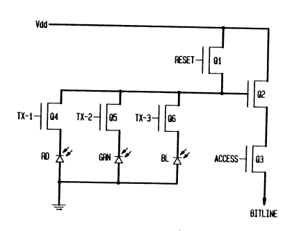
The components of the color pixel site according to
the present invention is shown in Figure 4. Sensing
elements RD, GRN and BL, preferably photodiodes configured
for sensing or capturing the red, green and blue color
spectrums, respectively, of a portion of the object to be
imaged in color. The sensing elements are each connected
through gating elements Q4, Q5 and Q6, respectively. Each
of the sensing element/gating element pair is connected in
parallel to the gate of a source follower, formed by
2156530
-- 6
transistors Q2 and Q3. The sensing and gating elements
also connect to power source Vdd through reset transistor
Q1. The transistors Q1 to Q6 are preferably CMOS
transistors. It is readily apparent to one skilled in the
art that bipolar transistors may also be used. In which
case, the source follower mentioned above is called an
emitter follower.
The operation of the active pixel color image sensor
of Fig. 4 is described with reference to the timing
diagram of Fig. 5. Each RD, GRN and BL photodiode is
first pre-charged by connecting each photodiode to Vdd, by
holding the reset signal high while pulsing each of the
gate transistors TX1 to TX3 as shown with timing "A".
During integration time period "B", a charge proportional
to the captured energy level irradiated from the
corresponding portion of the object is stored in each
photodiode. During read out period "C", the access line
is held high to turn on transistor Q3. The gate
transistors Q4, Q5 and Q6 are then activated in turn by
pulsing the TX-1, TX-2 and TX-3 lines. With the access
line and any of the gate input lines TX-1 to TX-3 held
high, any charge stored in any of the corresponding
photodiodes RD, GRN and BL is passed through the source or
emitter follower Q2 and Q3 of Figure 4 to the Bitline
output.
Advantageously, the active pixel image sensor
according to the present invention reduces the number of
components required for imaging with multiple sensing
elements and at the same time reduces the physical size of
each pixel site. The size reduction is multiplied when an
imaging array is formed by connecting a plurality of image
sensors.
Figure 6 shows the imaging array formed by connecting
a plurality of image sensors of Figure 4 in a plurality of
rows and columns. A controller 600, which includes a row
215~'j30
-
-- 7
decoder for accessing one row at a time, controls each row
of the array with control pulses activated substantially
in accordance with the timing as shown in Figure 5.
The reset and access lines are common to each row of
pixel sensors and there are three lines for each of the
red, green and blue gating controls. The output at the
Bitline output columns are connected to amplifier 610 for
amplifying the video signals. The row and column being
activated by the controller 600 is shown in dotted lines
in Figure 6.
It is readily apparent to one ordinarily skilled in
the art that the above descriptions of an active pixel
image sensor according to the present invention is
applicable for any active pixel image sensor having
multiple sensing elements. A color active pixel image
sensor is but one example of such multiple sensing element
device. As another example, the technique according to
the present invention may be equally applicable in a
monochrome application where two rows of sensing elements
share a single row of source followers to reduce the
physical size of the device in a similar manner.
Accordingly, the present invention may be embodied in
other specific forms without departing from the spirit or
essential characteristics of the invention as indicated in
the appended claims.