Note: Descriptions are shown in the official language in which they were submitted.
2156~37
BC9-94-110 1
LOW POWER RING DETECT FOR
COMPUTER SYSTEM WAKEUP
Eield of the Invention
The present invention relates generally to computer system
architecture and, more specifically, to a desktop computer system
having a system suspend/resume capability and low power ring detection
and ring confirmation for system wakeup.
Background of the Invention
Personal computer systems are well known in the art. Personal
computer systems in general, and IBM Personal Computers in particular,
have attained widespread use for providing computer power to many
segments of today's modern society. Personal computers can typically
be defined as a desktop, floor standing, or portable microcomputer
that is comprised of a system unit having a single central processing
unit (CPU) and associated volatile and non-volatile memory, including
all RAM and BIOS ROM, a system monitor, a keyboard, one or more
flexible diskette drives, a fixed disk storage drive (also known as a
"hard drive"), a so-called "mouse" pointing device, and an optional
printer. One of the distinguishing characteristics of these systems
is the use of a motherboard or system planar to electrically connect
these components together. These systems are designed primarily to
give independent computing power to a single user and are
inexpensively priced for purchase by individuals or small businesses.
Examples of such personal computer systems are IBM's PERSONAL COMPUTER
ATO and IBM's PERSONAL SYSTEM/l~ (IBM PS/l).
Personal computer systems are typically used to run software to
perform such diverse activities as word processing, manipulation of
data via spread-qheets, collection and relation of data in databases,
displays of graphics, design of electrical or mechanical systems using
system-design software, etc.
~ 2l56537
BC9-94-110 2
The first four related applications disclose a computer system
having four power management states: a normal operating state, a
standby state, a suspend state, and an off state. One switch is used
to change between the off state, the normal operating state, and the
suspend state.
The normal operating state of the computer system of the present
invention is virtually identical to the normal operating state of any
typical desktop computer. Users may use applications and basically
treat the computer as any other. One difference is the presence of a
power management driver, which runs in the background (in the BIOS and
the operating system), transparent to the user. The portion of the
power management driver in the operating system (OS) is the Advanced
Power Management (APM) advanced programming interface written by Intel
and Microsoft, which is now present in most operating systems written
to operate on Intel's 80X86 family of processors. The portion of the
power management driver in BIOS (APM BIOS) communicates with the APM
OS driver. The APM OS driver and the APM BIOS routines together
control the computer's transition to and from the other three states.
The second state, the standby state, uses less power than the
normal operating state, yet leaves any applications executing as they
would otherwise execute. In general, power is conserved in the
standby state by placing devices in their respective low-power modes.
For example, power is conserved in the standby state by ceasing the
revolutions of the fixed disk within the hard drive and by ceasing
generating the video signal.
The third state is the suspend state. In the suspend state,
computer system consumes an extremely small amount of power. The
suspended computer consumes very little power from the wall outlet.
The only power consumed is small amount of power to maintain the
circuitry that monitors the switch from a battery inside the computer
system (when the system is not receiving AC power) or a small amount
of power generated at an auxiliary power line by the power supply
(when the system is receiving AC power).
215G537
BC9-94-110 3
This small use of power is accomplished by saving the state of
the computer system to the fixed disk storage device (the hard drive)
before the power supply is turned "off." To enter the suspend state,
the computer system interrupts any executing code and transfers
control of the computer to the power management driver. The power
management driver ascertains the state of the computer system and
writes the state of the computer system to the fixed disk storage
device. The state of the CPU registers, the CPU cache, the system
memory, the system cache, the video registers, the video memory, and
the other devices' registers are all written to the fixed disk. The
entire state of the system is saved in such a way that it can be
restored without the code applications being adversely affected by the
interruption. The computer then writes data to the non-volatile CMOS
memory indicating that the system was suspended. Lastly, the computer
causes the power supply to stop producing power. The entire state of
the computer is safely saved to the fixed disk storage device, system
power is now "off," and computer is now only receiving a small amount
of regulated power from the power supply to power the circuitry that
monitors the switch.
The fourth and final state is the off state. In this state, the
power supply ceases providing regulated power to the computer system,
but the state of the computer system has not been saved to the fixed
disk. The off state is virtually identical to typical desktop
computers being turned off in the usual manner.
Switching from state to state is handled by the power management
driver and is typically based on closure events of a single switch, a
flag, and two timers: the inactivity standby timer and the inactivity
suspend timer. The system has a single power button. This button can
be used to turn on the computer system, suspend the state of the
system, restore the state of the system, and turn off the system.
More and more, modems and facsimile/modems are becoming part of
what is considered a standard PC system. In most systems for a user
to intercept facsimile messages or to allow people to connect to their
computer using the modem, the user must leave the computer on. Thus
~_ 2l56537
BC9-94-110 4
with typical systems, the user must forego any advantage of power
savings of the suspend state since there is no external method of
turning on the computer other than the power switch. The user can
place the computer in "standby" mode which does re~uire less power,
but energy is still wasted since the computer must have power supplied
to it for it to power an internal modem which can then answer the
phone. If the user is using a external modem, a computer system that
is off cannot detect a ring indicator supplied by the modem.
Typical systems implementing state transitions responsive to a
telephone ring have numerous problems. Such systems typically either
(i) use expensive, specialized integrated circuits having low power
modes, (ii) duplicate much of the modem ring circuitry, or (iii) leave
much of the computer system powered, which consumes more power than
necessary.
Critically, typical systems cause state transitions responsive to
many signals along the telephone line that are not true rings, such as
line tests or noise on the telephone line. Such spurious state
transitions can waste power and are an inconvenience to users.
Summary of the Invention
Under the present invention, the computer is modified so that it
has the capability of detecting a ring either directly from an
unpowered internal modem, or from a ring indicator from a powered
external modem, while the computer is an extremely low power state.
According the present invention, a microcontroller is constantly
executing code while the PC is plugged into a power outlet. The
microcontroller is powered by a custom power supply providing an
auxiliary 5 volt DC power source that is capable of being turned on
and off by a control line.
The microcontroller controls whether the rest of the computer
system is receiving regulated power from the power supply or not. One
input of the microcontroller is connected to the RING_IN from the
standard RS-232 serial port on the computer. When the microcontroller
21~6537
BC9-94-110 5
detects an active level on the signal, the microcontroller allows the
power supply to begin providing regulated to the computer system.
Another input of the microcontroller is tied to a standard modem ring
optoisolator of a standard internal modem modified to provide the
signal from the optoisolator via a cable.
The microcontroller performs two checks on the signal from the
optoisolator beyond merely detecting energy at a certain voltage
across Tip and Ring. First, the microcontroller is constantly sensing
this line for a signal within the frequency range that corresponds to
a valid ring signal. This check alone filters out many of the signals
that are detected as a ring by typical systems. When it detects a
ring in the defined frequency range, the microprocessor then
immediately causes the power supply to begin providing regulated power
to the computer system.
Second, once the power supply provides regulated power to the
system and the system boots, the BIOS performs another check.
Responsive to the microcontroller detecting a ring signal of the
proper frequency, the microcontroller immediately causes the power
supply to begin providing regulated power to the system. While the
hard drive is spinning up, the BIOS queries the modem whether the
modem has detected a ring also. If the modem ring detect circuitry
has also detected a ring, then the booting process continues. If the
modem did not detect a ring, then the system powers off.
The benefit of this approach is that the computer system can
enter the normal operating system responsive to a true ring and if the
appropriate software is enabled, the computer system can receive and
act upon the incoming data from the modem/serial port once state of
the system is restored. Thereafter, the system reenters either the
off state or the suspend state.
This system provides a remote access capability for the home PC
system without adding a second telephone line without adding a special
phone answering system and without adding significant cost to the
computer system. The user leaves this system off with one or more
application programs enabled and ready to perform requested tasks when
2156~37
BC9-94-110 6
it resumes. The user can call the phone number twice in quick
succession and establish a host connection. The first call wakes up
the system without triggering the asnwering machine; the second call
allows the system to answer and establish a host connect session,
again without triggering the answering machine.
This system also works with both internal and external modems.
In the alternative, the RING_IN line can also be used as an external
wake up from some other device such as a photo detector or a voice
recognition system. The external device need only set the line to an
active state for the computer system to turn on.
This system has extremely low power usage because the internal
modem does not have to be powered; only the power management
microcontroller need be powered.
These and other advantages of the present invention will become
more apparent from a detailed description of the invention.
Brief Description of the Drawings
In the accompanying drawings, which are incorporated in and
constitute a part of this specification, embodiments of the invention
are illustrated, which, together with a general description of the
invention given above, and the detailed description given below serve
to example the principles of this invention.
Figure 1 is a perspective view of a personal computer embodying
this invention;
Figure 2 is an exploded perspective view of certain elements of
the personal computer of Figure 1 including a chassis, a cover, an
electromechanical direct access storage device and a planar board and
illustrating certain relationships among those elements;
Figures 3A and 3B show a block diagram of certain components of
the personal computer of Figures 1 and 2;
Figure 4 is a state diagram of the computer system of the present
invention, showing the four system states: normal, standby, suspend,
and off;
21 $6$37
BC9-94-110 7
Eigure 5 is a block diagram showing the relevant portions of the
power supply;
Figure 6A is an electrical schematic diagram of the power
management circuitry of the present invention, showing the various
interfaces to other Figures;
Figure 6B is an electrical schematic diagram of the connection of
the power management circuitry to the internal modem;
Figure 6C is a waveform diagram showing the various signals
within the reset circuit for the power management circuitry;
10Figure 6D is an electrical schematic diagram of a second
embodiment of the power supply fault detection and correction circuit;
Figure 7 is a state diagram of one of the switch states
maintained by the power management processor of the present invention;
Figure 8 is a flow chart showing generally the power-up routine
15of the present invention;
Figure 9A is a flow chart showing the details of the Supervisor
Routine, which is called by the APM device driver in the operating
system approximately every second;
Figure 9B is a flow chart showing the details of the APM Working
20On Last Request Routine;
Figure 9C is a flow chart showing the details of the APM Reject
Last Request Routine;
Figure 10 is a flow chart showing the details of the Suspend
Routine of the present invention;
25Figure 11 is a flow chart showing the details of the Boot-Up
Routine of the present invention;
Figure 12 is a flow chart showing the details of the Resume
Routine of the present invention;
Figure 13 is a flow chart showing the details of the Save CPU
30State Routine of the present invention;
Figure 14 is a flow chart showing the details of the Restore CPU
State Routine of the present invention;
Figure 15 is a flow chart showing the details of the Save 8959
State Routine of the present invention;
2156537
BC9-94-110 8
Figure 16 is a flow chart showing the details of the Dynamic Save
File Allocation Routine of the present invention;
Figure 17 is a flow chart showing the details of the Exit Standby
Routine of the present invention;
Figure 18 is a flow chart showing the details of the Enter
Standby Routine of the present invention; and
Figure 19 is a flow chart showing the details of the Power
management Processor Routines of the present invention.
Detailed Description of the Preferred Embodiment
While the present invention will be described more fully
hereinafter with reference to the accompanying drawings, in which a
preferred embodiment of the present invention is shown, it is to be
understood at the outset of the description which follows that persons
of skill in the appropriate arts may modify the invention here
described while still achieving the favorable results of this
invention. Accordingly, the description which follows is to be
understood as being a broad, teaching disclosure directed to persons
of skill in the appropriate arts, and not as limiting upon the present
invention. The present invention deals with the complete design of a
computer system, including, but not limited to computer architecture
design, digital design, BIOS design, protected mode 80486 code design,
application code design, operating system code design, and Advanced
Power Management advanced programming interface usage. This
application is written for those very familiar with all aspects of
computer system design.
Referring now more particularly to the accompanying drawings, a
microcomputer system embodying the present invention is there shown
and generally indicated at lO (Figure 1). As mentioned hereinabove,
the computer 10 may have an associated display monitor 11, keyboard
12, mouse 13, and printer or plotter 14. The computer 10 has a cover
15 formed by a decorative outer member 16 (Figure 2) and an inner
shield member 18 which cooperate with a chassis 19 in defining an
enclosed, shielded volume for receiving electrically powered data
2156537
BC9-94-110 9
processing and storage components for processing and storing digital
data. At least certain of these components are mounted on a
multilayer planar 20 or motherboard which is mounted on the chassis 19
and provides a means for electrically interconnecting the components
of the computer 10 including those identified above and such other
associated elements as floppy disk drives, various forms of direct
access storage devices, accessory adapter cards or boards, and the
like. As pointed out more fully hereinafter, provisions are made in
the planar 20 for the passage of input/output signals to and from the
operating components of the microcomputer.
The computer system has a power supply 17, a power button 21,
also hereinafter the switch 21, and a power/feedback LED 23. Unlike
in the usual power switch in a typical system, the power button 21
does not switch AC line power to and from the power supply 17, as will
be explained below. The chassis l9 has a base indicated at 22, a
front panel indicated at 24, and a rear panel indicated at 25 (Figure
2). The front panel 24 defines at least one open bay (and in the form
illustrated, four bays) for receiving a data storage device such as a
disk drive for magnetic or optical disks, a tape backup drive, or the
like. In the illustrated form, a pair of upper bays 26, 28 and a pair
of lower bays 29, 30 are provided. One of the upper bays 26 is
adapted to receive peripheral drives of a first size (such as those
known as 3.5 inch drives) while the other 28 is adapted to receive
drives of a selected one of two sizes (such as 3.5 and 5.25 inch) and
the lower bays are adapted to receive devices of only one size (3.5
inch). One floppy disk drive is indicated at 27 in Figure 1, and is
a removable medium direct access storage device capable of receiving
a diskette inserted thereinto and using the diskette to receive, store
and deliver data as is generally known. One hard disk drive is
indicated at 31 and is a fixed medium direct access storage device
capable of storing and delivering data as is generally known.
Prior to relating the above structure to the present invention,
a summary of the operation in general of the personal computer system
10 may merit review. Referring to Figures 3A and 3B, there is shown
2156~37
BC9-94-110 10
a block diagram of a personal computer system illustrating the various
components of the computer system such as the system 10 in accordance
with the present invention, including components mounted on the planar
20 and the connection of the planar to the I/O slots and other
hardware of the personal computer system. Connected to the planar is
the system processor 40, also herein CPU 40, comprised of a
microprocessor, which is connected by a high speed CPU local bus 42
through a memory control unit 46, which is further connected to a
volatile random access memory (RAM) 53. The memory control unit 46 is
comprised of a memory controller 48, an address multiplexer 50, and a
data buffer 52. The memory control unit 46 is further connected to a
random access memory 53 as represented by the four RAM modules 54.
The memory controller 48 includes the logic for mapping addresses to
and from the microprocessor 40 to particular areas of RAM 53. This
logic is used to reclaim RAM previously occupied by BIOS. Further
generated by memory controller 48 is a ROM select signal (ROMSEL),
that is used to enable or disable ROM 88. While any appropriate
microprocessor can be used for system processor 40, one suitable
microprocessor is the 80486 which is sold by INTEL. The Intel 80486
has an internal cache, therefore, any CPU 40 that is an Intel 80486
will have a CPU cache 41.
While the present invention is described hereinafter with
particular reference to the system block diagram of Figures 3A and 3B,
it is to be understood at the outset of the description which follows
that it is contemplated that the apparatus and methods in accordance
with the present invention may be used with other hardware
configurations of the planar board. For example, the system processor
40 could be an Intel 80286 or 80386 microprocessor. As used herein,
reference to an 80286 or 80386 or 80486 generally intends such a
microprocessor as obtained from Intel. However, in recent times other
manufacturers have developed microprocessors which are capable of
executing the instruction set of the Intel X86 architecture, and usage
of the terms stated is intended to encompass any microprocessor
capable of executing that instruction set. As known to persons
21S6537
BC9-94-110 11
skilled in the applicable arts, early personal computers typically
used the then popular Intel 8088 or 8086 microprocessor as the system
processor. These processors have the ability to address one megabyte
of memory. More recently, personal computers typically use the high
speed Intel 80286, 80386, and 80486 microprocessors which can operate
in a virtual or real mode to emulate the slower speed 8086
microprocessor or a protected mode which extends the addressing range
from 1 megabyte to 4 Gigabytes for some models. In essence, the real
mode feature of the 80286, 80386, and 80486 processors provide
hardware compatibility with software written for the 8086 and 8088
microprocessors. Processors in the Intel family described are
frequently identified by a three digit reference to only the last
three digits of the full type designator, as "486".
Returning now to Figures 3A and 3B, the CPU local bus 42
(comprising data, address and control components, not shown) provides
for the connection of the microprocessor 40, a math coprocessor 44 (if
not internal to the CPU 40), a video controller 56, a system cache
memory 60, and a cache controller 62. The video controller 56 has
associated with it a monitor (or video display terminal) 11 and a
video memory 58. Also coupled on the CPU local bus 42 is a buffer 64.
The buffer 64 is itself connected to a slower speed (compared to the
CPU local bus 42) system bus 66, also comprising address, data and
control components. The system bus 66 extends between the buffer 64
and a further buffer 68. The system bus 66 is further connected to a
bus control and timing unit 70 and a DMA unit 71. The DMA unit 71 is
comprised of a central arbiter 82 and a DMA controller 72. An
additional buffer 74 provides an interface between the system bus 66
and an optional feature bus such as the Industry Standard Architecture
(ISA) bus 76. Connected to the bus 76 are a plurality of I/0 slots 78
for receiving ISA adapter cards (not shown). ISA adapter cards are
pluggably connected to the I/0 slots 78 and may provide additional I/0
devices or memory for the system 10.
~_ 2l56~37
BC9-94-110 12
An arbitration control bus 80 couples the DMA controller 72 and
central arbiter 82 to the I/O slots 78, a diskette adapter 84, and an
Integrated Drive Electronics (IDE) fixed disk controller 86.
While the microcomputer system 10 is shown with a basic 4
megabyte RAM module 53, it is understood that additional memory can be
interconnected as represented in Figures 3A and 3B by the addition of
optional higher-density memory modules 54. For purposes of
illustration only, the present invention is described with reference
to the basic four megabyte memory module.
A latch buffer 68 is coupled between the system bus 66 and a
planar I/O bus 90. The planar I/O bus 90 includes address, data, and
control components respectively. Coupled along the planar I/O bus 90
are a variety of I/O adapters and other components such as the
diskette adapter 84, the IDE disk adapter 86, an interrupt controller
92, an RS-232 adapter 94, nonvolatile CMOS RAM 96, also herein
referred to as NVRAM, a CMOS real-time clock (RTC) 98, a parallel
adapter 100, a plurality of timers 102, the read only memory (ROM) 88,
the 8042 104, and the power management circuitry 106. The 8042, shown
at 104, is the slave microprocessor that interfaces with the keyboard
12 and the mouse 13. The power management circuitry 106 is in circuit
communication with the power supply 17, the power switch 21, the
power/feedback LED 23, and an internal modem 900 and/or an external
modem 902. The external modem is typically connected to a transformer
904, which is connected to a typical wall outlet, as is known to those
skilled in the art. The modems 900, 902 are connected to a typical
telephone outlet. The power management circuitry 106 is shown in
Figure 6A and 6B and is more fully described in the text accompanying
Figures 6A, 6B, 6C, and 7. The read only memory 88 includes the BIOS
that is used to interface between the I/O devices and the operating
system of the microprocessor 40. BIOS stored in ROM 88 can be copied
into RAM 53 to decrease the execution time of BIOS. ROM 88 is further
responsive (via ROMSEL signal) to memory controller 48. If ROM 88 is
enabled by memory controller 48, BIOS is executed out of ROM. If ROM
88 is disabled by memory controller 48, ROM is not responsive to
21S6537
_
BC9-94-110 13
address inquiries from the microprocessor 40 (i.e. BIOS is executed
out of RAM).
The real-time clock 98 is used for time of day calculations and
the NVRAM 96 is used to store system configuration data. That is, the
NVRAM 96 will contain values which describe the present configuration
of the system. For example, NVRAM 96 contains information describing
the capacity of a fixed disk or diskette, the type of display, the
amount of memory, time, date, etc. Furthermore, these data are stored
in NVRAM whenever a special configuration program, such as SET
Configuration, is executed. The purpose of the SET Configuration
program is to store values characterizing the configuration of the
system to NVRAM.
Nearly all of the above devices comprise volatile registers. To
prevent the unnecessary cluttering of the drawings, the registers of
a particular device will be referenced to that device. For example,
the CPU registers will be referred to as the CPU 40 registers and the
video controller registers will be referenced as the video controller
56 registers.
As mentioned hereinabove, the computer has a cover indicated
generally at 15 which cooperates with the chassis 19 in forming an
enclosed, shielded volume for containing the above identified
components of the microcomputer. The cover 15 preferably is formed
with an outer decorative cover member 16 which is a unitary molded
component made of a moldable synthetic material and a metallic thin
sheet liner 18 formed to conform to the configuration of the
decorative cover member. However, the cover can be made in other
known ways and the utility of this invention is not limited to
enclosures of the type described.
States of Operation
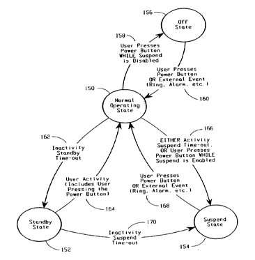
Referring now to Figure 4, a state diagram of the computer system
of the present invention is shown. The computer system 10 of the
present invention has four states: a normal operating state 150, a
standby state 152, a suspend state 154, and an off state 156. The
2l56~37
BC9-94-llO 14
transitions between the states shown in Figure 4 are meant to be
descriptive of the preferred embodiment, but not limiting.
Consequently, additional events may alternatively be used to cause
state transitions.
The normal operating state 150 of the computer system 10 of the
present invention is virtually identical to the normal operating state
of any typical desktop computer. Users may use applications and
basically treat the computer as any other. One difference,
transparent to the user, is the presence of a power management driver
in the operating system (the "APM OS driver"), which runs in the
background, and various APM BIOS routines. The APM BIOS routines are
discussed in the text below and include the Suspend Routine, the
Resume Routine, the Boot-Up Routine, the Supervisor Routine, the Save
CPU State Routine, and the Restore CPU State Routine. One APM BIOS
routine not shown on any of the Figures is the APM BIOS Routing
Routine. The APM BIOS Routing Routine essentially accepts commands
from the APM OS driver and calls the appropriate APM BIOS routine.
For example, when the APM OS driver issues the Suspend Command, the
APM BIOS Routing Routine calls the Suspend Routine. As another
example, whenever the APM OS driver issues the Get Event command, the
APM BIOS Routing Routine calls the Supervisor Routine. These routines
are located in BIOS and are shadowed when the BIOS is shadowed. The
power management driver in the OS and the APM BIOS routines control
the computer's transition between the four states. A reference to the
word "APM" by itself generally is a reference to the APM OS driver,
although the context may dictate otherwise.
The second state, the standby state 152, uses less electrical
power than the normal operating state 150, yet leaves any applications
executing as they would otherwise execute. In general power is saved
in the standby state 152 by the code placing devices into respective
low power modes. In the preferred embodiment, electrical power is
conserved in the standby state 152 by ceasing the revolutions of the
fixed disk (not shown) within the fixed disk storage device 31, by
ceasing generating the video signal, and by putting the CPU 40 in a
2156537
BC9-94-110 15
low power mode, as will be more fully explained below. However, this
is not intended to be limiting and other methods may be used to reduce
power consumption, such as slowing or stopping the CPU clock.
In the preferred embodiment, electrical power is conserved in
three separate ways. First, in the normal operating state 150, the
fixed disk within the fixed disk storage device 31 is constantly
spinning at, e.g., 3600, 4500, or 5400 revolutions per minute (RPM).
In the standby state 152, the IDE disk controller 86 is given the
command to cause the fixed disk storage device 31 to enter a low-power
mode (the fixed disk inside the fixed disk storage device 31 ceases
spinning), thereby conserving the power the motor (not shown) inside
the fixed disk storage device 31 typically consumes while spinning the
fixed disk.
Second, in the normal operating state 150, the video controller
56 of the computer system constantly generates a video signal (HSYNC,
VSYNC, R, G, B, etc. as is well known in the art) corresponding to the
image seen on the video display terminal 11. In the standby state 152
the video controller 56 ceases generating the video signal, thereby
conserving the electrical power normally consumed by the video
controller 56; HSYNC, VSYNC, R, G, and B are all driven to
approximately 0.00 VDC. Using a VESA (Video Electronics Standards
Association) compliant monitor allows further power savings because
VESA compliant monitors turn themselves off when HSYNC and VSYNC are
at approximately 0.00 VDC.
Third, in the normal operating state 150, the CPU 40 constantly
executes commands, thereby consuming electrical power. In the standby
state 152 the BIOS issues a HALT instruction in response to the APM
CPU Idle Call. Executing a HALT instruction significantly reduces CPU
power consumption until the next hardware interrupt occurs. When
truly idle, the CPU can remain halted more than 90% of the time.
Note that some systems have "screen-savers," which cause the
screen 11 to become dark to prevent phosphor burn-in of the front
surface of the video display terminal. In most of such systems, the
video controller 56 is still generating a video signal; it is merely
2l56537
BC9-94-110 16
generating a video signal corresponding to a dark screen or a dynamic
display. Thus, a computer system executing a screen-saver still
consumes the electrical power necessary to generate the video signal.
The third state is the suspend state 154. In the suspend state
154, computer system consumes an extremely small amount of electrical
power. The suspended computer consumes less than 100 milliwatts of
electrical power in the preferred embodiment. The only power consumed
is approximately 5 watts consumed due to inefficiencies in the power
supply 17 and a small amount of power used by the power management
circuitry 106.
This small use of electrical power is accomplished by saving the
state of the computer system to the fixed disk storage device (the
hard drive) 31 prior to turning the power supply "off.l' To enter the
suspend state 154, the CPU 40 interrupts any applications and
transfers program execution control of the CPU to the power management
driver. The power management driver ascertains the state of the
computer system 10 and writes the entire state of the computer system
to the fixed disk storage device 31. The state of the CPU 40
registers, the CPU cache 41, the system RAM 53, the system cache 60,
the video controller 56 registers, the video memory 56, and the
remaining volatile registers are all written to the fixed disk drive
31. The entire state of the system 10 is saved in such a way that it
can be restored without significant usability penalties. That is, the
user need not wait for the system to load the operating system, and
load the graphical user interface, and application programs as it
normally would.
The computer then writes data to the non-volatile CMOS memory 96
indicating that the system was suspended. Lastly, the CPU 40 commands
the microcontroller U2 to cause the power supply 17 to stop providing
regulated power to the system through the +5 VDC and +12 VDC lines.
The computer system 10 is now powered down with the entire state of
the computer safely saved to the fixed disk storage device 31.
The word "state" is used throughout this document in two similar,
but possibly confusing ways. Devices can be "in" a particular state.
,~_ 2l56537
BC9-94-110 17
The four system states--normal 150, standby 152, suspend 154, and off
156--refer to the general state of the computer system 10 of the
present invention. These "states" describe the computer system lO in
a general way. For example, while in the normal operating state 150,
the CPU 40 is still executing code and changing a plurality of
registers within the system 10. Likewise, similar activity occurs
while in the standby state 152. Thus, the memory and register
configuration of the computer system 10 is dynamic while the system 10
is in the normal operating state 150 and the standby state 152.
10Other devices can also be "in" certain states. The power
management circuitry 106 preferably uses a second processor as a power
management processor, such as a microcontroller U2 shown in Figure 6A,
to implement the various power management features. Many such
processors are suitable; in this particular embodiment, the power
15management processor is a preprogrammed 83C750 microcontroller. The
variables and pins of the microcontroller U2 can be in several states,
as will be explained in the text accompanying Figure 6A.
Contrast the above with the "state of" a device, for example, the
"state of the computer system 10" or the "state of the CPU 40." The
"state of" a device refers to the condition of that device at a
particular computer cycle. All memory locations and registers will
have particular binary values. The "state of" a device is a static
binary snapshot of the contents of that device.
The "state of" the computer system 10 refers to operational
equivalents and not necessarily exact copies. For example, a computer
system in a state A may have certain memory in either CPU cache 41 or
system cache 60. It is possible to "flush" the contents of either
cache back to the system RAM 53, putting the computer system in a
state B. Purely speaking, the state of the computer system in state
A is different from the state of the computer system in state B,
because the contents of cache and system RAM are different. However,
from a software operational perspective, state A and state B are the
same, because, aside from a slight decrease in system speed (caused by
the program not having the benefit of executing out of cache), the
2156~37
BC9-94-110 18
executing programs are not affected. That is, a computer in state A
and a computer in state B are software operationally equivalent, even
though the computer whose cache was flushed will experience a slight
decrease in performance until the cache areas are reloaded with
helpful code.
The word "power" is also used in two similar, but possibly
confusing ways. "Power" most often refers to electrical power.
However, "power" also refers to computational power occasionally. The
context should make the intended usage obvious.
A "circuit" is generally a reference to a physical electronic
device or a plurality of devices electrically interconnected.
However, the term "circuit" also is intended to encompass CPU code
equivalents of physical electronic devices. For example, on the one
hand, a two-input NAND gate can be implemented via a 74LS00 or,
equivalently, in a programmable device. These two devices are
physical electronic devices. On the other hand a NAND gate can also
be implemented by having the CPU 40 read two inputs from two CPU-
readable input ports, generate the NAND result using a CPU command,
and output the result via a CPU-writable output port. These CPU-
interfacable ports can be simple, such as decoded latches, or theirprogrammable device equivalent, or complex, such as PIAs, which are
well-known in the art. The term "circuit" is meant to be broad enough
to include all three examples of NAND gate implementations, above. In
some cases, "circuit" may refer to merely an electrical pathway. Types
of electrical pathways include a wire, a trace or via on a printed
circuit board, etc., or any combination of types of electrical
pathways that form a single electrically connected pathway.
A "signal" may refer to a single electrical waveform or a
plurality of waveforms. For example, the video controller generates
a video signal. The video signal is actually a plurality of signals
on a plurality of electrical conductors: HSYNC, VSYNC, R, G, B, etc.
as is well known in the art.
Returning now to Figure 4, the fourth and final state is the off
state 156. The off state 156 is virtually identical to any typical
~ 2156537
BC9-94-110 19
computer system that has been turned off in the ordinary sense. In
this state, the primary/regulation unit 172 of the power supply 17
ceases providing regulated power to the computer system 10, ~with the
exception of a small amount of regulated power through AUX5, as will
be more fully explained in the text accompanying Figure 5) but the
state of the computer system 10 has not been saved to the fixed disk
31. The suspend state 154 and the off state 156 are similar in that
the power supply 17 no longer generates regulated power. They differ
in that in the off state 156, the state of the computer system 10 is
not saved to the hard drive 31, as it is in the suspend state 154.
Moreover, when leaving the off state 156, the computer 10 "boots" as
if it is being turned on. That is, any executing code must be started
either by the user or automatically by a means such as the
AUTOEXEC.BAT file. However, when leaving the suspend state 154, the
computer 10 resumes executing where it was when it was interrupted.
Figure 4 also shows a general overview of the events that cause
transitions between the four states. These events will be further
explained in the text accompanying Figures 6 through 8; however, a
cursory explanation may be helpful. The power button 21, two timers
(the inactivity standby timer and the inactivity suspend timer, see
Figure 9 and accompanying text), a minutes to wake timer, and a
Suspend Enable Flag (see Figures 6A and 7 and accompanying text) all
affect which state the computer enters. In general, the two timers
can be either hardware or CPU code timers, executing on the CPU as a
program. In the preferred embodiment, they are both CPU code timers,
executing from the BIOS data segments. However, the two timers could
conceivably be hardware timers, which would be a better solution, in
that it would reduce the overhead of the system. The timers are more
fully explained in the text accompanying Figure 9. Both timers are
active when the computer 10 is in either the normal operating state
150 or the standby state 152. The timers are in communication with
other routines such that the expiration of either timer causes a
transition as outlined below. Either or both timers can be configured
to expire after a certain period of time, depending on the particular
2ls6s37
BC9-94-110 20
needs of the user. In the preferred embodiment, the inactivity
standby timer and the inactivity suspend timer can be set to expire
after 10 to 90 minutes. Either or both timers can be stopped, that
is, configured to never expire. "Stopping" the timers can take the
form of actually ceasing the incremental counting action of the timers
or merely ignoring their expiration. In the preferred embodiment,
setting a zero value in the timer expiration value causes the timer
expiration not to be tested. The user of a networked computer may,
for example, not want the computer to enter the suspend state 154
because doing so may cause the LAN to fail with respect to that
computer.
In theory, the timers can count up or count down and can be reset
to a fixed predetermined state and expected to count to another fixed
predetermined state when the timer is started (or restarted) or the
present value can be used and a difference or sum calculated as the
endpoint expiration trigger. In the preferred embodiment, when the
timers are reset, the present value of the minutes variable from the
real-time clock 98 is stored. The timers are checked for expiration
by subtracting the current minutes value from the saved minutes value
and comparing the difference to the values selected by the user.
Both timers are affected by certain system activity. For
example, in the preferred embodiment, user activity in the form of
keyboard 12 keys being pressed, the mouse 13 being moved, mouse 13
buttons being pressed, or hard drive 31 activity causes each timer to
be restarted, as more fully explained in the text accompanying Figure
9; therefore, while a user is pressing keyboard 12 keys or using the
mouse 13, or while an application is accessing the hard drive 31,
neither timer will expire. In addition other system events might be
used to reset the timers. Any of the hardware interrupts might
alternatively be monito,red for activity. Thus, it might be desirable
to have printing (IRQ5 or IRQ7) or a COMM port access (IRQ2 or IRQ3)
prevent the system from entering the suspend state 154.
The Suspend Enable Flag is a CPU-manipulable and readable latch
within the microcontroller U2, which will be more fully explained in
2156537
BC9-94-110 21
the text accompanying Figure 6A. In short, putting the
microcontroller U2 in one mode causes a press of the switch 21 to
place the system 10 into the off state 156 and putting the
microcontroller U2 into another mode causes a press of the switch 21
to place the system 10 into the suspend state 154. If the computer
system 10 is in the normal operating state 150 and the power button 21
is pressed while the Suspend Enable Flag written to the
microcontroller U2 is CLEARed, then the computer system 10 enters the
off state 156, as shown at 158. If the computer system 10 is in the
10off state 156 and the power button 21 is pressed, then the computer
system enters the normal operating state 150, as shown at 160. In
addition, several "external events," which are explained more fully
below, can cause the system to transition from the off state 156 to
the normal operating state 150.
15If the computer system 10 is in the normal operating state 150,
one event can cause the computer to enter the standby state 152: if
the inactivity standby timer expires, the computer system 10 will
change to the standby state 152, as shown at 162. In the alternative,
the system can provide a means, such as a dialog box, a switch, or
other input device, for the user to force the system into the standby
state immediately. While in the standby state 152, any system or user
activity of the kind previously described, including the user pressing
the power button 21, will cause the computer 10 to leave the standby
state 152 and re-enter the normal operating state 150, as shown at
25164.
Pressing the power button 21 causes the system to change from the
standby state 152 to the normal operating state 150 to prevent user
confusion. As mentioned above, while in the standby state, the
monitor 11 is blanked and the power/feedback LED 23 is either on or
blinking, depending on how the flags in the microcontroller U2 are
configured. A user approaching the system might notice that the
monitor 11 is blank and, thinking that the system is in the suspend
state 154 or the off state 156, press the power button 21 in an
attempt to cause the system to enter the normal operating state 150.
2l56s37
' -
BC9-94-110 22
If a press of the power button 21 causes the system to enter either
the suspend state 154 or the off state 156, then the user above will
have just either turned off or suspended the computer, which is
directly contrary to the user's intention. Therefore, when in the
standby state 152, a press of the power button 21 causes the system to
change from the standby state to the normal operating state. Even if
idle, the CPU 40 will soon test whether the switch was pressed.
Hardware interrupts remove the CPU 40 from the idle state
approximately 20 times per second; thereafter during the next APM Get
Event, the microcontroller U2 is queried to determine whether the
switch 21 was pressed.
If the computer 10 is in the normal operating state 150, two
events can cause it to enter the suspend state 154. First, if the
inactivity suspend timer expires, the computer system 10 will change
to the suspend state 154, as shown at 166. Second, the user can cause
the computer 10 to enter the suspend state 154 immediately by pressing
the power button 21 while the Suspend Enable Flag written to the
microcontroller U2 is SET, also shown at 166. In the alternative,
additionally, the APM driver can issue a suspend request via a "Set
Power State: Suspend" command, which causes the APM BIOS driver to
call the Suspend Routine. While in the suspend state 154, the user
changes to the normal operating state 150 by pressing the power button
21, as shown at 168.
In addition, several external events can be used to change the
system 10 from the suspend state 154 to the normal operating state
150, at 168, or from the off state 156 to the normal operating state
150, at 160. For example, a telephone ring detect circuit in the
microcontroller U2 in the circuitry of Figure 6A is configured to
cause the system 10 to leave the off state 156 or the suspend state
154 and enter the normal operating state 150 when an attached
telephone line rings. Such a feature is useful for a system receiving
telefax data or digital data. The system enters the normal operating
state responsive to the telephone ring, performs the preset functions,
such as accepting an incoming facsimile transmission, uploading or
~_ 2l56s37
BC9-94-110 23
downloading files, allowing remote access to the system, etc., and
enters the suspend mode again responsive to the expiration of the
Inactivity Suspend Timer, only consuming power while the system is in
the normal operating state.
Likewise the microcontroller U2 implements a minutes to wake
alarm counter, which allows an alarm-type event to cause the system 10
to leave the suspend state 154 or the off state 156 and enter the
normal operating state 150. Such a system is useful in sending
telefax or digital data at a certain time of day to take advantage of
lower telephone usage rates, and performing system maintenance
functions, such as backing up the system hard drive 31 with a tape
backup system. In the latter case, the minutes to wake alarm is set
to turn the machine on a fixed period of time before the scheduler
causes the tape backup program to be executed. In the alternative,
the APM BIOS scheduler can be used to cause the execution of the tape
backup program.
Lastly, if the computer system 10 is in the standby state 152 and
the inactivity suspend timer expires, then the computer 10 changes to
the suspend state 154 as shown at 170. The computer system 10 cannot
change back from the suspend state 154 to the standby state 152, but
may only transition to the normal operating state 150 as described in
the text accompanying transition 168.
Obviously, the computer system 10 cannot instantaneously change
states. In each transition from one of the four states, a certain
period of time will be required to make the necessary system changes.
The details of each transition period will be explained in the text
accompanying Figures 6 through 15.
System Hardware
Before discussing the details of the code executing on the CPU
40, it mày be helpful first to discuss the hardware required to
achieve the four states. A block diagram of the power supply 17 is
shown in Figure 5. The power supply 17 has two units: a control unit
174 and a primary/regulation unit 172. The power supply 17 has
2156537
BC9-94-110 24
several inputs: Line-In, which accepts either 115 VAC or 220 VAC from
a typical wall outlet, and ON, which controls the regulation activity
of the power supply 17. The power supply 17 has several outputs: AC
Line-Out, +5 VDC, +12 VDC, AUX5, GND, and POWERGOOD. The AC Line-Out
is 115 VAC that is typically passed to the electrical power input (not
shown) of the video display terminal 11. The control unit 174 accepts
the ON input and generates the POWERGOOD output. The
primary/regulation unit 172 selectively regulates the 115 VAC from the
Line-In input down to +5 VDC, +12 VDC. Whether the primary/regulation
10unit 172 regulates power at the +5 VDC and +12 VDC lines depends on
the value of ON, as interfaced by the control unit 174. In the
preferred embodiment, the control unit 174 should provide isolation
for the circuitry generating the ON signal using, for example, an
appropriate optoisolator.
15The Line-In input and the AC Line-Out, +5 VDC, +12 VDC, GND, and
POWERGOOD outputs are well known in the art. When the power supply 17
is "off," that is, not providing regulated voltages from the Line-In,
the POWERGOOD signal is a logical ZERO. When the power supply 17 is
"on," the power supply 17 generates the +5 VDC and +12 VDC regulated
voltages from the 115 VAC Line-In. These four regulated voltages and
their associated GND are the "system power" as is commonly known in
the art. When the regulated voltages attain levels within acceptable
tolerances, the POWERGOOD signal changes to a logical ONE. Whenever
either the +5 or +12 Volt lines fall out of tolerance, the POWERGOOD
signal becomes a logical ZERO, thereby indicating this condition.
The AUX5 output provides an auxiliary +5 VDC to the planar. When
the power supply 17 is plugged into a typical wall outlet supplying a
nominal 115 VAC, the primary/regulation unit 172 provides regulated +5
VDC at AUX5, whether the power supply is "on" or "off." Thus, while
receiving AC power, the power supply 17 is always providing a nominal
+5 VDC at AUX5. The AUX5 output differs from the +5 output in that
the primary/regulation unit 172 only generates regulated +5 VDC
through the +5 output while the power supply 17 is "on." The AUX5
output further differs from the +5 output in that in the preferred
2156537
BC9-94-110 25
embodiment, the primary/regulation unit 172 supplies several amps of
current at +5 VDC through the +5 output, while the primary/regulation
unit 172 supplies less than an amp at +5 VDC though the AUX5 output.
Typical prior power supplies use a high-amperage double-throw
switch to connect and disconnect the Line-In input to and from the
regulation section of the power supply. The power supply 17 in the
present invention does not use a high-amperage double-throw switch.
Rather, the switch 21 controls circuitry that generates the ON signal.
In the preferred embodiment, the switch 21 is a momentary single pole,
single throw pushbutton switch; however, those skilled in the art
could adapt the circuitry of Figure 6A to make use of other types of
switches such as a single-pole, double throw switch. The AC Line-In
is always connected to the primary/regulation unit 172 from the wall
outlet. When ON is a logical ONE (approximately AUX5, nominally +5
VDC), the primary/regulation unit 172 does not regulate the 115 VAC
Line-In to +5 VDC or +12 VDC through the +5 or +12 outputs. The
primary/regulation unit 172 merely provides a low-amperage nominal +5
VDC at the AUX5 output. On the other hand, when ON is a logical ZERO
(approximately GND), the primary/regulation unit 172 does regulate the
115 VAC Line-In to +5 VDC and +12 VDC through the four +5 and +12
outputs, respectively. Thus, when ON is a ONE, the power supply 17 is
"off" and when ON is a ZERO, the power supply 17 is "on."
If specified, power supplies having an AUX5 output and an ON
input, like the power supply 17 described above, can be obtained from
suppliers of more conventional power supplies.
Referring now to Figure 6A, a schematic drawing of the electronic
circuitry of the computer system 10 of the present invention is shown.
The circuitry in Figure 6A is responsible for interfacing between the
switch 21, the power/feedback LED 23, the power supply 17, the video
display terminal 11, and code executing on the CPU 40.
The circuitry comprises four (4) integrated circuits--Ul, a first
preprogrammed PAL16L8; U2, a preprogrammed 83C750 microcontroller; U3,
a 74LS05, which is well known in the art; and U4, a second
preprogrammed PAL16L8 (not shown)--and the various discrete components
2I56537
BC9-94-110 26
in circuit communication as shown in Figure 6A. In general, the PALs
U1 and U4 (not shown) interface between the planar I/O bus 90 of
Figures 3A and 3B and the microcontroller U2, which interfaces to the
remaining circuitry of Figure 6A, which interfaces to the switch 21,
the power supply 17, the video display terminal 11, and a programmable
clock synthesizer 906. The clock synthesizer 906 can be one of many
such devices known to those of ordinary skill in the art. One such
part is the CH9055A, which is manufactured by Chrontel, and widely
available from numerous sources.
The circuitry of Figure 6A further comprises the switch 21, a 16
MHz crystal Yl, eighteen resistors Rl-R18, eight capacitors C1-C8,
three N-type MOSFETs Ql-Q3, which are standard low-current NMOS FETs
suitable for acting as a logic switch in the preferred embodiment, and
six (6) lN4148 small signal diodes CRl-CR6, all configured and
connected as shown in Figure 6A. The resistors Rl-R18 are ~ Watt
resistors and are of values shown in Figure 6A, + 5%. The capacitor
C1 is a 10 ~F (+ 10%) electrolytic capacitor. The capacitors C2 & C3
are 22 pF (+ 10%) tantalum capacitors. The capacitors C4-C8 are 0.1
~F (+ 10%) ceramic capacitors. Finally, the capacitor C9 is a 1000 pF
(+ 10%) ceramic capacitor.
The crystal Yl and the capacitors C2 and C3 generate signals used
by the microcontroller U2 to control the timing of operations, as is
known in the art. The diodes CRl and CR3 and the resistor R14 isolate
the AUX5 signal from the VBAT signal, while at the same time allowing
the AUX5 signal to supplement the VBAT signal in that while the power
supply 17 generates the AUX5 signal, the battery 171 is not drained.
Rather, the AUX5 signal is stepped down through the diodes CR1 and CR3
to supply the proper voltage to the devices connected to VBAT. In the
alternative, the VBAT line is isolated from the AUX5 line.
The second PAL U4 (not shown) is connected to address lines SA(l)
through SA(15) and the AEN (address enable) line. SA(l) through
SA(15) and AEN are part of the planar I/O bus 90 shown in Figures 3A
and 3B. ~ The second PAL U4 is programmed to be merely an address
decoder, presenting an active low signal DCD# when a predetermined
2156537
BC9-94-110 27
address is presented on address lines SA(1) through SA(15) and the AEN
(address enable) line is active. In this particular embodiment, the
second PAL U4 is preprogrammed to decode two consecutive 8-bit I/O
ports at addresses OECH and OEDH. In the alternative, the DCD# signal
can be generated by another electronic device, such as a memory
controller or an ISA controller chipset, as is known to those skilled
in the art.
The first PAL Ul is programmed to provide several functions: (i)
a read/write interface between the CPU and the microcontroller U2 to
allow commands and data to be transferred between the CPU 40 and the
microcontroller U2, (ii) a logical ORing of the mouse interrupt INT12
and the keyboard interrupt INTl; and (iii) a reset output to reset the
microcontroller U2 responsive to commands from the CPU 40.
The first PAL Ul makes use of two consecutive I/O ports, also
herein referred to as the "power management ports." The first PAL Ul
has eight (8) inputs from the planar I/O bus 90: SD(4), SD(0), SA(O),
IOW#, IOR#, RST_DRV, IRQl, and IRQ12. The first PAL Ul is reset to a
known initial condition by the active high signal RST_DRV input at pin
7 (I6), which is generated by the memory controller 46, as is well
known to those skilled in the art.
A reset line RST751 of the microcontroller U2 is at pin 9. A
reset subcircuit 920 is responsible for generating the RST751 signal
and comprises the four resistors R4, R16, R17, and R18, the two
capacitors Cl and C8, and the two MOSFETS Q2 and Q3, in circuit
communication with the first PAL U1 and the microcontroller U2 as
shown in Figure 6A. The reset subcircuit 920 interfaces the reset
output signal RESET from the first PAL U1 to the reset input signal
RST751 of the microcontroller U2 such that when the RESET line is at
a logical ONE, the RST751 line is pulled to a logical ONE, thereby
resetting the microcontroller U2.
The first PAL Ul resets the microcontroller U2 responsive to the
CPU 40 writing a logical ONE to bit 0 of control port OEDH. Writing
a logical ONE to bit O of control port OEDH causes the first PAL U1 to
pull the RESET line to a logical ONE, which pulls the RST751 line to
2156537
BC9-94-110 28
a logical ONE, thereby resetting the microcontroller U2. The CPU 40
clears the reset request by writing a logical ZERO to bit O of control
port OEDH.
In addition, the reset subcircuit pulls the RST751 line to a
logical ONE, thereby resetting the microcontroller U2, whenever the
voltage of AUX5 signal raises by a given amount, as would occur after
the AUX5 voltage lowers during a "brownout" or "blackout" of the AC
source to the power supply 17 occurs, as shown in Figure 6C. The
manufacturer of the 83C750, Philips, suggests using a simple RC
circuit to prevent reset problems; however, a simple RC circuit can
allow the 83C750 to latch up during power supply brownouts. In the
particular configuration of Figure 6A, the RST751 line is pulled to a
logical ONE for a period of time determined by R17 and C8 (thereby
resetting the microcontroller U2) when the AUX5 voltage raises by a
threshold amount in a period of time greater than the time constant
determined by R4, R16, and C1. This would occur after a typical
brownout or blackout. The threshold value is approximately 1.5 VDC in
the embodiment shown in Figure 6A.
Referring now to Figure 6C waveforms for the reset circuit 920
are shown for a period of time as AUX5 rises as AC power is applied to
the power supply 17 and a period of time during which a "brownout"
occurs. Before tO, the power supply is not generating AUX5, VBAT is
at approximately 3.3 Volts, Q3 is conducting and pulling the RST751
line to ground. At tO, the power supply begins generating AUX5 and
the voltage begins rising at a rate based on the load and the
capacitors in the power supply affecting AUX5. Nodel, the node
between C1 and R4, is capacitively coupled to AUX5; therefore, it
rises as AUX5 rises.
At tl, Nodel reaches approximately 1.5 Volts, which is sufficient
to trigger Q2, which pulls Node2 to ground. At t2, as Node2 passes
2.5 Volts, Q3 ceases conducting and the RST751 line jumps to the level
of AUX5 via R18 and rises with AUX5 to approximately 5 Volts. As the
RST751 line becomes approximately 3 Volts, the microcontroller U2 is
reset.
2156~37
BC9-94-110 29
At t3, AUX5 stops rising, therefore, Nodel stops rising and
begins discharging to ground (the RESET line of the first PAL U1 is
LOW) at a rate determined by C1 and R4. At t4, as Nodel passes
through approximately 1.5 Volts, Q2 stops conducting and Node2 charges
at a rate determined by C8 and R17. At t5, as Node2 passes
approximately 2.5 Volts, Q3 conducts, pulling the RST751 line to
ground. Thus, the reset on power-on is complete; the system is
usually in the state with AUX5 at 5 Volts, VBAT at 3.3 Volts, and
Nodel at ground and Node2 at VBAT.
At t6, a brownout starts at the AUX5 line and AUX5 discharges.
Being capacitively coupled to AUX5, Nodel tries to follow AUX5, but
cannot, because diodes in the first PAL U1 prevent it from going much
lower than -0.5 Volts. At t7, AUX5 is at its lowest point and starts
rising again. Again, Nodel follows AUX5 and rises. At t8, Nodel
reaches approximately 1.5 Volts, which is sufficient to trigger Q2,
which pulls Node2 to ground. At t9, as Node2 passes 2.5 Volts, Q3
ceases conducting and the RST751 line jumps to the level of AUX5 via
R18 and rises with AUX5 to approximately 5 Volts. As the RST751 line
becomes approximately 3 Volts, the microcontroller U2 is reset.
At tlO, AUX5 stops rising, therefore, Nodel stops rising and
begins discharging to ground (the RESET line of the first PAL Ul is
LOW) at a rate determined by Cl and R4. At tll, as Nodel passes
through approximately 1.5 Volts, Q2 stops conducting and Node2 charges
at a rate determined by C8 and R17. At tl2, as Node2 passes
approximately 2.5 Volts, Q3 conducts, pulling the RST751 line to
ground. Thus, the brownout-induced reset cycle is complete. Notice
that during this particular brownout, Nodel did not rise above 3 Volts
and, therefore, could not have reset the microcontroller if connected
to the RST751 pin. However, the voltage of AUX5 lowered below 4
Volts, which would have been enough to cause the microcontroller U2 to
enter an undefined state.
The threshold for triggering a reset is tied to the reference
value; therefore, to raise or lower the threshold voltage, the value
of the reference (in this case VBAT), must be raised or lowered,
2156537
BC9-94-110 30
respectively. The reset circuit provides the benefits of increased
reset protection for the microcontroller U2, while being very
inexpensive and consuming virtually no power when not resetting the
microcontroller U2.
Referring back to Figure 6A, the microcontroller U2 is interfaced
to the CPU 40 via the first PAL Ul and has a number of inputs,
outputs, and internally controllable functions.
The SWITCH signal is input at pin 8 (PO.O) and reflects the
current state of the pushbutton 21. The pushbutton 21 is normally
open. While the pushbutton 21 is open, the SWITCH line is pulled to
a logical ZERO (ground) through resistor R1. When the pushbutton 21
is pressed, thereby causing a closure event, the SWITCH line is pulled
up to a logical ONE (AUX5) through resistor R13. Capacitor C6 acts to
debounce the switch closure event; any further debouncing of closure
events of the switch 21 are performed within the microcontroller U2 by
reading the SWITCH a predetermined number of times, e.g., 50 times,
and assuring that the SWITCH line is the same for all those reads, as
is known to those skilled in the art.
The regulation of the power supply 17 is directly controllable by
the microcontroller U2. As shown in Figure 6A, the ON signal is
output at pin 5 (P3.0) and is wire-ORed with the SWITCH signal via
resistor R6 to control the ON# signal of the power supply. When the
ON signal is a logical ONE, MOSFET Q1 conducts, thereby pulling the
ON# line (pin 2 of JP2) to a logical ZERO (GND), thereby causing the
power supply 17 to begin providing regulated power to the system
through the +5 VDC and +12 VDC lines. On the other hand, when the ON
line is a logical ZERO, MOSFET Ql does not conduct, therefore the ON#
line (pin 2 of JP2) is pulled to a logical ONE (AUX5) by resistor R7,
thereby causing the power supply 17 to cease providing regulated power
through the +5 VDC and +12 VDC lines.
The state of the ON line is controlled by the microcontroller U2
responsive to a closure event of the switch 21 and responsive to the
CPU 40 via a writable register bit within the microcontroller U2,
which can be written by the CPU 40. The microcontroller U2 is powered
2156537
BC9-94-110 31
by AUX5; therefore, the microcontroller U2 is always powered,
executing code, and controlling the system. If the power supply 17 is
not providing regulated power to the system through the +5 VDC and +12
VDC lines and either (i) the switch 21 is pressed or (ii) one of the
external events occurs, then the microcontroller U2 asserts the ON
signal, thereby causing the power supply 17 to provide regulated power
to the system through the +5 VDC and +12 VDC lines. The
microcontroller continues asserting the ON signal after the switch 21
is released.
As a backup system, the power supply 17 can also be turned on
under the direct control of the user via the pushbutton 21. This
option will typically only be used if the microcontroller U2 ceases
functioning as expected, as will be evidenced by the system not
powering up responsive to a press of the power button 21. As shown in
Figure 6A, the switch 21 also controls the ON# line of the power
supply 17 via the diode CR2, the MOSFET Q1, the resistor R7, and the
connector JP2. Normally the pushbutton 21 is open and the SWITCH line
is pulled to a logical ZERO through Rl and MOSFET Q1 does not conduct;
therefore the ON# line (pin 2 of JP2) is pulled to a logical ONE
(AUX5) by resistor R7, and the power supply 17 is not providing
regulated power through the +5 VDC and +12 VDC lines. When the
pushbutton 21 is pressed and held by the user, the SWITCH line is
pulled to a logical ONE and MOSFET Ql conducts, thereby pulling the
ON# line (pin 2 of JP2) to a logical ZERO (GND), thereby causing the
power supply 17 to begin providing regulated power through the +5 VDC
and +12 VDC lines. With the button 21 still held in, after the system
is powered, the BIOS causes the CPU 40 to test whether the
microcontroller U2 is still functioning. If not, the CPU 40 resets
the microcontroller U2, which, after being reset, detects that the
switch 21 is being pressed. Consequently, with the button 21 still
held, the microcontroller asserts the ON signal and the user can
finally release the switch 21 with the knowledge that the
microcontroller is now controlling the power supply 17. To use this
backup option, the user must press the button 21 for a period of time
2156537
BC9-94-110 32
on the order of seconds--approximately two seconds after the logo
appears.
The microcontroller U2 only turns off the system responsive to
either (i) the switch 21 being pressed or (ii) the CPU 40 commanding
the microcontroller to turn off the system. To the microcontroller,
these events are the same, because the microcontroller is configured
such that a switch press can be caused either by a closure event of
the switch 21 or by the CPU 40; a hardware button press/release is
treated virtually the same as a software button press/release. The
microcontroller U2 only turns off the system without a command by the
CPU if the Suspend Enable Flag in the microcontroller U2 is cleared.
In this case, when the system is powered and the Suspend Enable Flag
is CLEARed, responsive to a closure event of the switch 21, the
microcontroller U2 clears the ON signal, thereby causing the power
supply 17 to cease providing regulated power to the system through the
+5 VDC and +12 VDC lines. The ON signal remains cleared after the
switch 21 is released.
The microcontroller U2 also turns off the system responsive to a
command by the CPU, as would be issued after a the system state has
been successfully saved to the hard disk drive (suspended).
Responsive to such a command, the microcontroller U2 clears the ON
signal, thereby causing the power supply 17 to cease providing
regulated power to the system through the +5 VDC and +12 VDC lines.
The microcontroller U2 can also detect and affect the system when
certain external events occur. The EXT_RING signal is input at pin 7
(PO.l) and allows the microcontroller U2 to detect a ring from the
powered external modem 902. As known to those skilled in the art,
typical external modems supply a ring signal that toggles to a logical
ONE in the well known RS-232C format when a ring signal is detected
across the tip and ring telephone lines. This signal is interfaced to
the microcontroller U2 via diode CR6 and divided with resistors R10
and R11 and finally input into the microcontroller U2 via the EXT_RING
line. The toggling signal is sampled every 25 milliseconds and
analyzed by the microcontroller U2, which deems that a ring is present
215~537
BC9-94-110 33
whenever this input is a logical ONE for two consecutive samples.
Responsive to this condition being met, the microcontroller U2 asserts
the ON signal, thereby causing the power supply 17 to being providing
regulated power to the system through the +5 VDC and +12 VDC lines.
For the EXT_RING signal to be used to detect an incoming telephone
call, an externally powered modem 902 must be present.
In the alternative, another device that provides a binary signal
conforming to the RS-232 specification (or close enough that it
asserts the EXT_RING signal) can be interfaced to the EXT_RING line
and used to awaken the system, for example, motion sensors, burglar
alarm sensors, voice activated sensors, light sensors, infrared light
sensors, "clapper" type sensors, etc.
As shown in Figures 6A and 6B, the present embodiment also has a
provision for detecting a telephone ring signal from an internal modem
900 having an optoisolator OPTO1 based ring-detect circuit. Many
suitable optoisolators are manufactured by e.g., Hewlett Packard, and
widely available from numerous sources. The internal modem 900 can
either be designed into the circuitry of the system planar 20 or
placed into one of the expansion slots 78. In the latter case, the
modem 900 must be modified to provide a Berg or similar connector to
allow the signal from the optoisolator OPTO1 to be electrically
connected to the circuitry of the power management circuitry of Figure
6A. Many manufacturers of modems are modifying their internal modems
to provide a connector suitable for use with the circuitry of the
present invention. The EXT_WAKEUP# signal is input at pin 4 (PO.2) of
the microcontroller U2 and is used to input a signal from the ring-
detect optoisolator OPTOl from the internal modem 900. This signal is
interfaced via resistors Rg and R5, diode CR6, and capacitor C9 and
finally input into the microcontroller U2 via the EXT_WAKEUP# line.
The threshold and protection portion 905 of the internal modem
900 is connected to the standard Tip and Ring telephone lines, and (i)
provides protection from lightning and other electrical events that
might damage the modem 900 and (ii) sets the ring threshold voltage,
as known to those skilled in the art of modem design.
2156537
BC9-94-110 34
The toggling signal from the optoisolator OPTOl is detected and
analyzed by the microcontroller U2, which deems that a ring is present
whenever three (3) consecutive signal periods of the signal on
EXT_WAKEUP have a frequency of between 15.1 Hz and 69.1 Hz. Unlike
the EXT_RING signal circuit, which must be powered to provide the ring
signal along EXT_RING, the internal modem 900 need not be powered for
the optoisolator OPTOl to supply a suitable signal along the
EXT_WAKEUP# line, which is normally pulled up to AUX5 by R5.
The microcontroller U2 can interrupt the CPU 40 via the CPU's
system management interrupt (SMI), if the CPU 40 has an SMI (the CPU
40 need not have an SMI for the system to take advantage of many of
the benefits of the present invention). The SMI_OUT# signal is output
at pin 3 (P3.2) of the microcontroller U2 and allows the
microcontroller U2 to immediately interrupt the CPU 40 without waiting
for the operating system to validate or otherwise allow the interrupt.
The state of the SMI_OUT# line is controlled by a writable register
bit, which can be written by the CPU 40, located within the
microcontroller U2. In addition the microcontroller U2 can assert the
SMI_OUT# signal and thereby interrupt the CPU 40 (i) responsive to
activity being detected on the ACTIVITY# line or (ii) before the
microcontroller U2 causes the power supply 17 to stop providing
regulated power to the system. Either or both of these events can be
enabled and disabled by commands from the CPU to the microcontroller
U2.
Each SMI, the microcode in the CPU 40 saves the state of the CPU
to the special CPU state save area to or from memory. Thereafter, the
CPU 40 executes the SMI interrupt handler, which performs the
functions below. To restore the state of the CPU, the SMI interrupt
handler issues the RSM (resume) instruction, which causes the CPU 40
to restore its own state from the special save area.
Before the CPU 40 causes the microcontroller U2 to interrupt the
CPU 40 via the CPU's SMI, the CPU 40 writes a value to a variable in
CMOS NVRAM indicating the reason for the SMI. This value in CMOS
NVRAM defaults to OOH, which indicates to the CPU 40 that the
2I56537
'_
BC9-94-110 35
microcontroller U2 is interrupting the CPU 40 asynchronously, as
occurs before the microcontroller U2 causes the power supply 17 to
stop providing regulated power. After each SMI, the CPU 40 sets that
variable in CMOS NVRAM to OOH. Responsive to this value, the CPU 40
performs certain tasks under the assumption that the system is going
to be powered down imminently by the microcontroller U2. The CPU 40
can extend the period of time before which the microcontroller U2
powers down the system by periodically restarting the power down
extend timer within the microcontroller U2.
During this period of time before the system powers down, the CPU
40 can perform numerous tasks. For example, since the user may have
changed one or more of the parameters that affect the wake alarm, the
CPU recalculates and writes to the microcontroller U2 a fresh minutes
to wake value. In addition, the CPU writes to the CMOS NVRAM certain
information that is to be written to the hard drive 31 later, such as
the period of time the computer system was operating since its last
power on.
Other values written by the CPU 40 include OlH, which indicates
that the CPU 40 is to jump to the Suspend Routine at 254; 02H, which
indicates that the CPU 40 is to jump to the Resume Routine at 454; and
OFFH, which indicates that the CPU 40 is to set up the special CPU
state save area in the segment EOOOH data structure.
In the present embodiment, the microcontroller is given control
over blanking the display 11. The DISP_BLANK signal is output via pin
1 (P3.4) of the microcontroller U2 and directly controls the blanking
of the display 11. Two inverters U3D and U3E interface the DISP_BLANK
signal with the ESYNC# and BLANK# lines. With the ESYNC# and BLANK#
lines at a logical ONE ~VCC), the video controller 56 generates a
video signal. When BLANK# and ESYNC# are at a logical zero (GND) the
video controller 56 ceases generating the video signal. The state of
the DISP_BLANK line is controlled by a writable register bit, which
can be written by the CPU 40, located within the microcontroller U2.
The CPU 40 instructs the microcontroller U2 to blank the display when
the system enters the standby state 152. In addition, the DISP_BLANK
2156537
BC9-94-110 36
line is sequentially SET then CLEARed responsive to closure events of
the switch 21. Similarly, activity at any one of the activity
interrupts, in this case INTl and INT12, causes the microcontroller to
CLEAR the DISP_BLANK line, thereby allowing the video controller 56 to
generate the video signal.
In addition, the microcontroller U2 controls the frequency of the
clock signals generated by the clock synthesizer 906. Three Berg-type
jumpers (not shown) JPO, JPl, and JP2 control the clock synthesizer as
follows: when JPO=O, JPl=l, and JP2=0, the clock synthesizer generates
a 33 MHz clock signal; when JPO=l, JPl=l, and JP2=0, the clock
synthesizer generates a 25 MHz clock signal; and when JPO=O, JPl=l,
and JP2=1, the clock synthesizer generates an 8 MHz clock signal. The
clock synthesizer 906 is further controlled by three clock lines CLKO,
CLKl, and CLK2, which correspond to JPO, JP1, and JP2. As shown in
Figure 6A, these clock lines CLKO, CLKl, and CLK2 are controlled by
the microcontroller U2 via the CLK_SLOW# signal, which is output at
pin 2 (P3.3) of the microcontroller U2. As shown, the CLK_SLOW#
signal is doubly inverted by the inverters with open collector outputs
U3A, U3B, and U3C. Also, resistors R15 and R8 are pullup resistors
used to pull the open collector output of U3A and the CLKO input to
the clock synthesizer 906 to a logical ONE, respectively.
The three clock signals CLKO, CLK1, and CLK2 and the three
jumpers JPO, JP1, and JP2 control the clock synthesizer as follows:
when the CLK_SLOW# signal is a logical ONE, the CLK1 and CLK2 signals
are also a logical ONE and, consequently, the clock synthesizer 906 is
controlled by the jumpers JPl, JP2 and generates the higher 25 MHz or
33 MHz clock signal for use by the system. On the other hand, when
the CLK_SLOW# signal is a logical ZERO, the CLKl and CLK2 signals are
also a logical ZERO and, consequently, the clock synthesizer 906
generates the lower 8 MHz signals for use by the system, thereby
causing the system to consume less power. As shown in Figure 6A, a
Berg-type jumper separates the CLK_SLOW# line from the CLKO line. If
a jumper is in place, the CLKO line follows the CLK_SLOW# signal. On
the other hand, if no jumper is in place, the CLKO line remains pulled
2156537
`'`,~
BC9-94-110 37
to a logical ONE by resistor R8 regardless of the state of the
CLK_SLOW# signal. The state of the CLK_SLOW# line is controlled by a
writable register bit, which can be written by the CPU 40, located
within the microcontroller U2. In addition, the CLK_SLOW# line can be
cleared by the microcontroller U2 in response to activity at the
ACTIVITY# line. As is apparent to those skilled in the art, other
clock synthesizers can be used in the present invention; the
interconnections between the microcontroller U2 and the clock
synthesizer might need to be changed to match the specific
specifications of the particular synthesizer used.
Additionally, the microcontroller U2 directly controls the
illumination of the power/feedback LED 23. The LED_CNTRL signal is
output at pin 22 (P3.6) and allows direct control of the
power/feedback LED 23 by the microcontroller U2. The resistors R2 and
R3 and diodes CR4 and CR5 allow the power/feedback LED 23 to be driven
by either the AUX5 power line or the VCC power line in response to the
LED_CNTRL line being at a logical ZERO. When the LED_CNTRL line is at
a logical ONE, the power/feedback LED 23 is not illuminated. As
described more fully below, the state of the LED_CNTRL line is
controlled by the microcontroller U2 in response to a closure event of
the switch 21, in response to the wake alarm, in response to one or
more rings at either ring-detect input, or in response to the system
being placed in the standby mode.
The microcontroller U2 can control the LED 23 to be a simple
power LED. As such, the LED 23 is illuminated after a closure event
of the switch 21 that causes the system to change from either the off
state 156 or the suspend state 154 to the normal operating state 150.
Likewise, the microcontroller U2 extinguishes the LED 23 after a
release event of the switch 21 that causes the system to change from
the normal operating state 150 to either the suspend state 154 or the
off state 156.
In addition, the LED 23 can be selectively flashed at a
particular rate, e.~., every second, by the microcontroller U2 to
indicate that the system is in the standby state 152. In addition,
2156537
BC9-94-110 38
the LED 23 can be selectively flashed at a different rate, e.q., every
half-second, by the microcontroller U2 to indicate that the system was
awakened by a ring or by the alarm and the system is in either the off
state or the suspend state. In the alternative, while in the suspend
state, the LED 23 can be selectively flashed in groups of flashes by
the microcontroller U2 to indicate the number o times the system was
powered up by external events, such as a ring, alarm, etc., and was
powered back down by the expiration of the inactivity suspend timer.
In this case, the BIOS is provided with one or more functions to allow
the OS and application programs to modify the number of times the
microcontroller U2 is to flash the LED 23. For example, if the system
is awakened by a ring and an incoming facsimile transmission is
received, the telecommunications application program can call the
particular BIOS function to add one to the number of flashes.
Thereafter, the BIOS causes the CPU 40 to write the new flash value to
the microcontroller U2, which then causes the LED 23 to flash the
commanded number of times.
The POWERGOOD signal is input at pin 4 (P3.1) of the
microcontroller U2 and allows this signal to be used by the
microcontroller U2 and the CPU 40. Specifically, the microcontroller
uses the POWERGOOD signal to implement a feedback-based fault
detection and correction circuit to determine if the power supply 17
has faulted and to clear the faulted condition. As described
elsewhere in this specification, if the ON signal has been asserted
for a period of time (e.g., three seconds) and the POWERGOOD signal is
at a logical zero, indicating that the power supply 17 is not
providing regulated voltages at proper levels, then the
microcontroller U2 assumes that the power supply 17 has faulted from,
e.a., an overcurrent condition. Consequently, to possibly clear the
faulted condition, the microcontroller U2 ceases asserting the ON
signal for a period of time (e.g., five seconds) to allow the fault to
clear. Thereafter, the microcontroller U2 reasserts the ON signal and
waits for the POWERGOOD signal to become a logical ONE, indicating
that the power supply 17 is now providing regulated power to the
2156537
BC9-94-110 39
system. Without this feedback-based fault detection and correction,
the power supply 17 would remain faulted and the microcontroller U2
would continue to assert the ON signal in an attempt to cause the
power supply 17 to begin generating regulated power. The only
solution would be to remove AC power from the power supply to clear
the fault.
An alternative embodiment of the power supply fault detection and
correction circuit is shown in Figure 6D. This embodiment uses four
FETs Q10-Q13, resistors R20-R23, a capacitor C20, and a 74HC132 to
detect when the power supply 17 is faulted and clear the fault. Q12
pulls the ON signal LOW for a period of time determined by R22 and
C20, when the ON signal is HIGH, AUX5 is being powered, and VCC is
below the threshold for triggering Q11, thereby clearing the fault
condition in the power supply.
The ACTIVITY# signal is input at pin 19 (INT1) of the
microcontroller U2 and is used by the microcontroller U2 to respond to
activity at the keyboard 12 and mouse 13. IRQ1 is the keyboard
hardware interrupt signal, which is input at pin 8 (I7) of the first
PAL U1; pressing a key on the keyboard 12 causes the IRQ1 signal to
pulse. IRQ12 is the mouse hardware interrupt signal, which is input
at pin 11 (I9) of the first PAL U1; moving the mouse 13 or pressing a
button on the mouse 13 causes the IRQ12 signal to pulse. The IRQ1 and
IRQ12 signals are logically Ored in the first PAL U1 and output as the
ACTIVITY# signal. Using the ACTIVITY# signal allows the
microcontroller U2 to never miss activity of either the keyboard 12 or
the mouse 13.
While in the standby state, activity on either interrupt causes
the microcontroller to restore immediately the video display. Using
the interrupts IRQ1 and IRQ12 in this manner gives the user immediate
feedback in the form of a restored video display when returning from
the standby state 152 to the normal operating state 154. Without it,
the user might not receive feedback until possibly seconds later when
the APM checks for user activity, as explained in the text
accompanying Figure 9.
2156537
I
BC9-94-110 40
Communications between the CPU 40 and the microcontroller U2 are
performed using SD(O), which is input at pin 18 (I/06) of the first
PAL Ul and input to the microcontroller U2 via the RWDO line, which is
output at pin 13 (I/03) of the first PAL U1 and input at pin 13 (Pl.O)
of the microcontroller U2, SD(1), which is input at pin 14 (pl.l) of
the microcontroller U2, SD(2), which is input at pin 15 (pl.2) of the
microcontroller U2, SD(3), which is input at pin 16 (pl.3) of the
microcontroller U2, SD(4), which is input at pin 6 (I5) of the first
PAL Ul, IO_STROBE#, which is input at pin 18 (INTO) of the
microcontroller U2, and PROC_RDY, which is output at pin 20 (Pl.7) of
the microcontroller U2. The first PAL Ul and the microcontroller U2
are configured and programmed to provide (i) four-bit parallel writes
from the CPU 40 to the microcontroller U2 along SD(O) via RWDO, SD(l),
SD(2), and SD(3), with one address being essentially a one-bit write
to reset the microcontroller U2 and the other being a nibble written
to the microcontroller U2 that is only valid when data bit SD(4) is
HIGH, and (ii) serial (one-bit) reads from the microcontroller U2 by
the CPU 40 along SD(O) via RWDO, with one address corresponding to the
ætatus bit and the other corresponding to the data bit from the
microcontroller U2.
Referring now to Figure 19, several of the routines executing on
the microcontroller U2 are shown beginning at 1160. The
microcontroller U2 is usually executing one of two main routines: the
Power On Routine, at tasks 1168 through 1216, or the Power Off
Routine, at tasks 1260 through 1308. The Power On Routine is executed
by the microcontroller U2 when the power supply 17 is providing
regulated power at the +5 and +12 lines or power supply 17 is not
providing regulated power at the +5 and +12 lines, but the system is
in the process of powering on. The Power Off Routine is executed by
the microcontroller U2 when the power supply 17 is not providing
regulated power at the +5 and +12 lines or the power supply 17 is
providing regulated power at the +5 and +12 lines, but the system is
in the process of powering off. In addition, there are three
interrupt-driven routines: one for communicating with the CPU 40, at
2l56s37
BC9-94-110 41
1220 through 1232, one for detecting activity of the mouse 13 or
keyboard 12, at 1236 through 1244, and one that provides a time-base
with 25 millisecond, half-second, second, and minute resolutions, at
1248 through 1256.
First, the microcontroller U2 is initialized, at 1164, during
which time all the variables are initialized, the counter variables
are initialized, the timer interrupt is initialized and enabled, and
external interrupts, which control the communication routine and the
activity routine, are initialized.
The communication routine is an interrupt-driven routine
beginning at 1220 that executes responsive to the IO_STROBE line being
pulled to a logical ZERO by the first PAL Ul, which indicates that the
CPU 40 is beginning a command or query. In short, this routine
receives a one- or more nibble command or query from the CPU 40, at
1224, implements the command and/or returns the data responsive to the
query, at 1228, and returns program execution control to the
interrupted code, at 1232.
The microcontroller sequentially receives the nibbles from the
CPU that form the command or query. After receiving a nibble, the
microcontroller pulls the PROC_RDY LOW. When it is ready for the next
nibble, it pulls PROC_RDY HIGH again. Upon seeing this LOW to HIGH
transition at PROC_RDY, the CPU 40 then can write the next command
nibble.
While the microcontroller U2 is implementing the command or query
from the CPU 40, it cannot receive another command; therefore, the
microcontroller U2 asserts the PROC_RDY line to a logical ZERO,
indicating to the CPU 40 (via reads of the status port) that the
microcontroller cannot accept the next command/query yet. When the
implementation is finished, the PROC_RDY line is asserted at a logical
ONE, indicating to the CPU 40 (via reads of the status port) that the
microcontroller U2 is ready to accept the next command/query.
The activity routine is an interrupt-driven routine beginning at
1236 that executes responsive to the ACTIVITY# line being pulled to a
logical ZERO by the first PAL U1, which inaicates that the user has
2156~37
BC9-94-110 42
used either the mouse 13 or the keyboard 12. In short, responsive to
receiving the interrupt, this routine (i) SETs a bit indicating that
there was either mouse 13 or keyboard 12 activity, ~ii) restores the
clock speed if clock slowing is enabled, (iii) unblanks the screen 11
if blanking is enabled, (iv) restarts the failsafe timer, and (v)
generates an SMI to the CPU, if enabled, at 1240. Thereafter, the
routine returns program execution control to the interrupted code, at
1244. The bit set by this routine is then queried by the Supervisor
Routine every APM "get event," as detailed elsewhere in this
specification.
The timer routine is an interrupt-driven routine beginning at
1248 that executes responsive to the internal timer interrupt, which
is based on a 16-bit free-running counter configured to generate the
interrupt every 25 milliseconds to provide a time-base for the
microcontroller U2. The timer routine provides the following time-
bases: 25 milliseconds, half-seconds, seconds, and minutes. In short,
this routine receives the interrupt, determines when the various times
have occurred, performs the appropriate activity, at 1252, and returns
program execution control to the interrupted code, at 1256.
Every tick (every 25 milliseconds), if the power supply is not
providing regulated power and the microcontroller is configured to
respond to rings, the timer routine checks for an RS-232 ring on the
EXT_RING line and SETs a bit if one occurred.
Every half-second while in either the off state or the suspend
state, the timer routine determines whether it should toggle the LED
23 to implement the awake on external ring indicator flashing
sequence, detailed elsewhere in this specification.
Every second while in either the standby state, the timer routine
determines whether it should toggle the LED 23 to implement the
suspend indicator flashing sequence, detailed elsewhere in this
specification.
Also, every second, the timer routine decrements the failsafe
timer, decrements the APM fail-suspend timer, and decrements the power
supply fault timer, if appropriate, and SEIs a corresponding bit if
2l56537
BC9-94-110 43
any have expired. The failsafe timer is a 20-second timer that causes
the microcontroller to turn the system power off when it expires. The
failsafe timer is frequently restarted (reset) by the Supervisor
Routine in response to APM get events; therefore, as long as the code
executing on the CPU 40 is executing properly, the failsafe timer
never expires. However, if the code ceases executing properly, the
failsafe timer expires and, responsive to a press and release of the
power button 21, the microcontroller U2 causes the power supply 17 to
stop providing regulated power at the +5 and +12 lines under the
assumption that the BIOS and other routines have failed.
The APM fail-suspend timer is an 18-second timer that is enabled
when the switch 21 is in the off/release state (indicating that the
user is trying to turn the system off) and that causes the system to
attempt to suspend when it expires, hopefully before the faiLsafe
timer expires, causing the microcontroller to turn the system off.
Like the failsafe timer, the APM fail-suspend timer is frequently
restarted (reset) by the code executing on the CPU 40, e.g., APM Get
Events, APM Working on Last Request, and APM Reject Last Request;
therefore, as long as the code executing on the CPU 40 is executing
properly, the APM fail-suspend timer never expires. However, if the
code ceases executing properly, the APM fail-suspend timer expires.
When the APM fail-suspend timer expires, the microcontroller U2
SETs a bit. This bit is checked during each timer level 0 interrupt,
which occurs approximately every 55 milliseconds, as is known to those
skilled in the art. In addition, the timer level 0 interrupt service
routine restarts the failsafe timer. If the timer level 0 interrupt
service routine detects that the APM fail-suspend timer has expired,
it jumps to the Suspend Routine in an attempt to suspend the system,
as described in the text accompanying Figure 10.
The suspend started by the timer level 0 interrupt service
routine is not the preferred method of suspending. Many application
programs and adapters are APM aware and perform tasks in response to
the system being suspended. A suspend started by the timer level 0
interrupt service routine cannot use APM to indicate to these APM
2156537
-
BC9-94-110 44
aware entities that a suspend is imminent. Consequently, the system is
suspended without these entities being properly prepared. As such, the
system will be saved by a suspend started by the timer level O
interrupt service routine, therefore data in memory will not be lost;
however, the user may need to reboot the machine to place the system
into its proper state after saving the desired data.
The APM fail-suspend timer is particularly helpful in patching
"holes" in the APM driver in the OS. For example, when a Microsoft
Windows 3.1 modal dialog box is displayed, the Windows APM driver
ceases issuing APM get events. Conse~uently, if a modal dialog box is
displayed when the user presses the power button 21 in an attempt to
suspend the system, the system will not suspend. The microcontroller
U2 will notice that the switch is in the off/release state, but the
Supervisor Routine will not be called because all APM get events have
ceased. The switch press will not be acted upon until the modal dialog
box is cleared by the user. However, once the APM fail-suspend timer
expires and its expiration is detected by the timer level O interrupt
service routine, the system state will be saved to the extent possible
without indicating to APM aware entities that the system is being
suspended.
Every minute, the timer routine decrements the minutes to wake
alarm timer and the activity timer. When the minutes to wake timer
expires, if enabled, the microcontroller causes the power supply 17 to
begin providing regulated power at the +5 and +12 lines.
After the microcontroller U2 is initialized, the power supply is
tested, at 1168, to determine whether the power is off. If the power
is still on, the microcontroller 17 checks to see of the power supply
17 is faulted, at 1172. The power supply 17 has several internal
protections that cause it to shut down or "fault." The microcontroller
U2 determines whether the power supply 17 is faulted as follows: if
the microcontroller is operating (indicating that AUX5 is powered,
i.e., AC power is being provided to the power supply 17), AND the
microcontroller U2 is asserting the ON signal in an attempt to cause
the power supply 17 to provide regulated power at the +5 and +12
2156S37
_,
BC9-94-110 45
lines, AND the POWERGOOD line is not asserted (indicating that the
power supply 17 is not providing regulated power at the +5 and +12
lines), then the power supply 17 is faulted and must be reset.
At task 1172, the power supply 17 is actually tested twice. The
microcontroller U2 asserts the ON signal and then waits for three
seconds, as measured by the internal time-base. If the POWERGOOD
signal is not asserted after ON has been asserted for three seconds,
then the microcontroller U2 clears the ON signal and waits for another
five seconds. Then it asserts the ON signal again and waits for
another three seconds. If the POWERGOOD signal is not asserted after
ON has been asserted for three seconds, then the microcontroller U2
clears the ON signal deems the power supply 17 faulted.
If the power supply is faulted, the microcontroller U2 jumps to
the Power Off Routine, as indicated at 1174. On the other hand, if
the power supply is not faulted or is off, the microcontroller causes
the power supply 17 to begin providing regulated power at the +5 and
+12 lines, at 1175, and initializes the I/O ports, turns on the LED
23, and enables external interrupts, at 1176.
Figure 7 shows the switch state machine maintained within the
microcontroller U2. As shown in that figure, the states change in
response to closure events of the switch 21 and other events, such as
resetting of the computer system 10 and writes by the CPU 40. With
AUX5 not being provided by the power supply 17, the microcontroller U2
is not being powered and, therefore, the switch state is meaningless,
at 174. A press of the switch 21, a telephone ring from either
source, the minutes to alarm timer expiring, and a command from the
CPU 40 cause microcontroller to cause the power supply 17 to begin
providing system power, as described in the text accompanying Figure
6.
As shown in Figure 7, the switch 21 has four states monitored by
the microcontroller U2~ the on/press state 176 (in which the user
is holding in the button and is trying to turn on the machine), (ii)
the on/release state 178 (in which the user has released the button
and is trying to turn on the machine), (iii~ the offjpress state 180
2156~37
BC9-94-llO 46
(in which the user is holding in the button and is trying to turn off
the machine), and (iv) the off/release state 182 (in which the user
has released the button and is trying to turn off the machine). Next,
at 1180, the microcontroller U2 tests whether the switch is in the
off/release state, indicating that the user has released the button
and is trying to turn off the machine.
When in state 174 and the switch 21 is pressed, the
microcontroller U2 enters the on/press switch state 176. Releasing
the switch 21 causes the microcontroller U2 to enter the on/release
switch state 178. Similarly, when the microcontroller U2 is reset, the
microcontroller U2 enters the on/release state 178. Pressing the
switch 21 again causes the microcontroller U2 to enter the off/press
switch state 180. Releasing the switch 21 again causes the
microcontroller U2 to enter the off/release switch state 182.
Subsequent closures of switch 21 causes the microcontroller U2 to
cycle through the four states, as shown in Figure 7. The
microcontroller U2 is in the on/release switch state 178 when the
computer system lO is in the normal operating state 150. Application
programs will execute while in that state. The system 10 may enter and
leave the standby state 152 in that state. This state also
corresponds to a user-generated suspend abort request. The off/release
switch state is the switch state corresponding to a suspend request by
the user. That is, starting with the system in the off state 156,
pressing and releasing the switch 21 once places the computer system
in the normal operating state 150. Pressing and releasing the switch
21 once again generates a suspend request, which is read by the
Supervisor Routine, which is discussed more fully in the text
accompanying Figure 9. Pressing and releasing the switch 21 a third
time, before the system 10 is in the suspend state 154, generates a
suspend abort request, which is read by the Suspend Routine.
Referring back to Figure 19, if the user has released the button
and is trying to turn off the machine, then the microcontroller U2
jumpæ to the Power Off Routine, as indicated at 1184.
2156537
BC9-94-110 47
On the other hand, if the button is in the off/press state,
indicating that the user is holding in the button and is trying to
turn off the machine, then, the microcontroller tests whether the
switch has been masked by the BIOS, at 1192. The BIOS masks the
switch 21 once on entry into standby to prevent a switch press from
forcing the system from the standby state to the suspend state, to
prevent user confusion, as explained elsewhere.
If the switch 21 has been masked by the BIOS, then the
microcontroller code jumps back to task 1176 and clears the mask bit
to allow the next switch press to cause the system to enter either the
off state or the suspend state. On the other hand, if the switch 21
has not been masked, or if the switch 21 is not in the off/press
state, the microcontroller executes the heartbeat routine, at 1196.
The heartbeat routine is used to indicate to the CPU 40 that the
microcontroller U2 is functioning properly. The CMD_STATE# line output
of the microcontroller (pin 17, P1.4) is normally a logical ONE. Every
50-60 microseconds, the microcontroller U2 pulls that line to a
logical ZERO for approximately 1.5 microseconds and then raises it
back to a logical ONE. Since the power management status port read by
the CPU 40 is the logical AND of the CMD_STATE# and PROC_RDY lines,
this transition from HIGH to LOW and back to HIGH can monitored every
so often by the CPU 40, e.q., as the system boots, to ensure the
microcontroller U2 is functioning properly.
Next, the microcontroller U2 tests whether the BIOS has commanded
a power-off, at 1200. The CPU 40 can access and alter virtually every
variable in the microcontroller U2. If the BIOS has set the variable
indicating that the system should be powered off, as e.q., after the
state of the system is written to the hard drive 31 during a suspend,
the microcontroller U2 jumps to the Power Off Routine, as indicated at
1204.
On the other hand, if the BIOS has not commanded a power off,
then the microcontroller executes the Failsafe Routine, at 1208. The
failsafe timer is a 20-second timer that is enabled when the power
supply 17 is providing regulated power at the +5 and +12 lines. This
2156537
BC9-94-110 48
routine checks whether the failsafe timer has expired and SETs a bit
if it has. This routine also restarts the failsafe timer if commanded
by the BIOS to do so.
Next, at 1212, as a safety measure and to synchronize the
microcontroller to the power supply 17, the microcontroller checks the
POWER_GOOD line to detect whether the power supply 17 is still
providing regulated power at the +5 and +12 lines.
If the power supply 17 is not providing regulated power at the +5
and il2 lines, then the microcontroller U2 jumps to the Power Off
Routine, as indicated at 1216. On the other hand, if the power supply
17 is providing regulated power at the +5 and +12 lines, then the
microcontroller code jumps back to task 1180 and continues execution.
The Power Off Routine begins at task 1260. First, the
microcontroller U2 disables the activity interrupt at 1264 to prevent
the display from being unblanked.
Next, at 1268, the microcontroller checks the POWER_GOOD line to
detect whether the power supply 17 is still providing regulated power
at the +5 and +12 lines. If the power supply 17 is providing
regulated power at the +5 and +12 lines, then the microcontroller U2
tests whether the display should be blanked and/or the LED 23 turned
off, at 1272. If so, the microcontroller U2 causes the video
controller 56 to cease generating the video signals and/or turns off
the LED 23.
Thereafter, or if the LED and display are not to be blanked, the
microcontroller next tests whether (i) the BIOS has commanded that the
system should be turned back on by setting a bit, or (ii) the user has
commanded that the system should be turned back on by pressing the
power button 21 again. If either of these have occurred, then the
system is to be powered back up and the microcontroller U2 jumps to
the Power On Routine, as indicated at 1284.
Next, the microcontroller determines whether a ring has occurred
at the EXT_WAKEUP# line from the optoisolator OPTO1. With the RS-232
line this involves merely checking if the EXT_RING line is HIGH. For
the signal from the optoisolator OPTO1, this involves more checking by
2156537
BC9-94-110 49
the microcontroller U2. The EXT_WAKEUP# line is normally pulled HIGH
by the resistor R5. The optoisolator OPTOl pulls this line LOW when
the voltage across Tip and Ring is higher than the voltage threshold
set by the threshold and protection portion 905, ~, 60 V, as when
the telephone line rings. However, this condition can also be met when
the phone line is tested or from noise on the line. Therefore, merely
waiting for a LOW at the EXT_WAKEUP# line might permit a false "ring"
to awaken the system.
Consequently, the microcontroller determines whether the signal
is a ring by measuring the frequency of the ring. A ring within
standards is a signal between 16 Hz to 58 Hz. The microcontroller U2
measures the three periods of time between four rising edges of the
EXT_WAKEUP# signal and if all three correspond to a frequency of
between 15.1 Hz and 69.1 Hz, the microcontroller U2 deems th~t a
proper ring has occurred at that line and SETs a corresponding bit.
The checking routine is started by a LOW being detected at the
EXT_WAKEUP# line. If that line is LOW for three consecutive reads,
then the microcontroller U2 waits for the line to return HIGH for
three consecutive reads. Immediately thereafter, the 16-bit counter
that forms the basis for the timer interrupt is read and the value
stored and the microcontroller U2 waits for the line to transition LOW
for three consecutive reads. The microcontroller next tests whether
the time between the first two rising edges is between 15 milliseconds
and 66 milliseconds, indicating that the signal is between 15.1 Hz and
69.1 Hz. If so, the high-resolution counter is sampled again and the
microcontroller calculates the difference between the two counter
samples as it waits for the next LOW to HIGH transition. The process
repeats for the next two LOW to HIGH transitions on the EXT_WAKEUP#
line. If all three periods of time are within the range, then the
microcontroller U2 deems that a proper ring has occurred at that line
and SETs a corresponding bit. If there is no LOW at the EXT_WAKEUP#
line or if any of the periods of time are out of that range, the
microcontroller code continues without setting the bit.
2156537
BC9-94-llO 50
Next, the microcontroller tests whether there has been a ring or
the minutes to wake alarm has expired, at 1286. For the RS-232 ring,
the optoisolator ring, or the minutes to wake alarm, this involves the
microcontroller U2 testing whether the associated bit is SET.
If either there has been a ring or the minutes to wake alarm has
expired, then the system is to be powered back on and the
microcontroller U2 jumps to the Power On Routine, as indicated at
1287.
Thereafter, at 1288, the microcontroller tests whether the power
supply 17 is providing regulated power at the +5 and +12 lines. If
not, the code jumps back to task 1280 and begins the loop again. On
the other hand if the power supply 17 is providing regulated power at
the +5 and +12 lines, then the microcontroller U2 executes the
heartbeat routine, at 1292, and the failsafe routine, at 1296. These
two routines were discussed in the text accompanying tasks 1196 and
1208, respectively.
The microcontroller U2 only causes the power supply 17 to stop
providing regulated power at the +5 and +12 lines under three
situations: (i) the BIOS has commanded an immediate power-off, which
is implemented in the communications routine, (ii) the failsafe timer
has expired, or (iii) the user presses the power button and the
Suspend Enable flag in the microcontroller U2 is not SET, a condition
for which the microcontroller U2 tests every time the SWITCH input is
read. Therefore, the microcontroller tests whether the failsafe timer
has expired, at 1300. If not, the code jumps back to task 1280 and
begins the loop again.
On the other hand, if the failsafe timer has expired, indicating
that the system is to be powered down, the microcontroller U2
generates an SMI to the CPU 40, at 1304, if enabled. This allows the
CPU to perform certain tasks under the assumption that the system is
going to be powered off immediately thereafter. For example, the CPU
40 recalculates and writes to the microcontroller U2 an updated
minutes to wake alarm value.
~_ 2l56~37
BC9-94-110 51
If no further action is taken by the CPU 40, the microcontroller
powers off the system after a programmable SMI timer expires. The CPU
40 can extend this period of time by restarting the SMI timer by
writing an appropriate value to the microcontroller U2.
Thereafter, and if the test at 1268 indicates that the power
supply is not supplying good power, the microcontroller U2 powers the
system down, at 1308. This involves (i) causing the power supply 17 to
stop providing regulated power at the +5 and +12 lines, (ii) disabling
the communications interrupt since the CPU 40 is about to lose power,
(iii) setting the output ports (except ON) HIGH to minimize their
power consumption (SWITCH, EXT_RING, EXT_WAKEUP, etc. can still be
read by the microcontroller U2 in this mode), (iv~ setting the power-
off variable so the remaining routines are aware that the power to the
system is off, and (v) changing the switch state to off/release so
that the next switch press will turn the system back on.
Thereafter, the code jumps back to task 1280 and begins the loop
again, waiting for a ring, for a switch press, for the BIOS to command
it to awaken the system, or for the minutes to wake alarm to expire.
System Software
Having described the hardware aspects of the computer system 10
of the present invention, the code aspects remain to be described.
Referring now to Figure 8, a general overview of the power-up
routine is shown. The routine starts at 200 when the CPU jumps to and
executes the code pointed to by the Reset Vector. This occurs each
time the CPU is powered up and whenever the ~PU is reset by either a
reset hardware signal or when a RESET instruction is executed by
jumping to the code pointed to by the reset vector. Such reset
procedures are well known in the art.
First of all, the flow of the Power Up Routine depends on why the
machine was powered up. As will be explained in more detail in the
text accompanying ~igure 11, the system 10 might have been powered up
by a brownout or blackout. As such, it would be improper to allow the
system to remain on. Therefore, the Power Up Routine first determines
2156537
BC9-94-110 52
if the system should remain on, at 940. If the system was improperly
powered up, then the CPU 40 commands the microco~troller U2 to cause
the power supply to stop providing regulated power to the system, at
942.
One test performed in determining whether the system is to remain
powered is to confirm that the telephone line is ringing if the system
was powered up responsive to what the microcontroller thought was a
ring. Specifically, after powering the system up, if the system was
awakened in response to a ring, while the system waits for the hard
disk within the hard drive 31 to spin up, the CPU 40 queries the modem
900 or 902 which are now fully powered) whether it detects a ring
signal as well. If not, then the system powers down. If the modem 900
or 902 also detects a ring signal, then the system is to remain the
booting process continues.
Assuming the system is to remain powered, in general, the flow of
the Power-Up Routine depends on whether the system is in the off state
156 or the suspend state 154. That is, whether the Suspend Flag is
cleared or set, respectively, in CMOS NVRAM 96. As shown at 202, the
system 10 determines whether it is in the off state 156 or the suspend
state 154 by reading a Suspend Flag from the nonvolatile CMOS memory
96. When the system leaves the normal operating state 150 to either
the off state 156 or the suspend state 154, each routine either SETs
or CLEARs the Suspend Flag in NVRAM 96. If the Suspend Flag is SET in
NVRAM 96, then the computer system 10 is in the suspend state 154 and
the state of the computer system 10 was stored in the fixed disk
storage device 31. On the other hand, if the Suspend Flag is CLEAR in
NVRAM 96, then the computer system 10 is in the off state 156 and the
state of the computer system 10 was not stored in the fixed disk
storage device 31. Thus, if the Suspend Flag is SET in NVRAM 96, then
the computer executes a "normal" boot routine, shown at tasks 204-210.
The first task is the power-on self-test (POST), as shown at 204,
which will be explained more fully in the text accompanying Figure 11;
after returning from the POST, the CPU 40 calls the PBOOT routine to
load the operating system, as shown at 206.
~ 2ls6537
BC9-94-110 53
The PBOOT routine is a typical routine that runs on IBM
computers, with slight variations, which will be explained below.
PBOOT determines from where to boot (either from the hard drive 31 or
from a disk inside the floppy drive 27) and loads the operating
system, which analyses and implements system changes as instructed by
the CONFIG.SYS file, and finally executes the AUTOEXEC.BAT batch file.
The PBOOT routine is well known in the art. The OS loads an APM
device driver, which queries the BIOS whether the BIOS is APM aware.
If so, the BIOS APM routine and the OS APM routine perform a
handshaking and thereafter cooperate to provide the various features
described herein. The operating system executes code indefinitely, as
instructed by the user, as shown at 210. However, the consequence of
informing the API of the Supervisor Routine is that the APM BIOS and
APM OS cause the Supervisor Routine to execute in "parallel" with the
executing programs, as indicated at 212. That is, the system 10 is a
time-multiplexed multitasking system and the APM Get Event, and
consequently the Supervisor Routine, are executed periodically. The
end result is that the Supervisor Routine is executed approximately
every second. The Supervisor Routine will be explained fully in the
text accompanying Figure 9. After the normal boot routine 204-210 is
finished, the computer system 10 is in the normal operating state 150,
as discussed in the text accompanying Figure 4.
Referring again to task 202, if the Suspend Flag is SET in NVRAM
96, then the system state was saved to the hard drive 31 and the
system 10, performs a resume boot routine, shown at tasks 214-220.
First, the system, executes an abbreviated POST, as indicated at 214.
The abbreviated POST will be explained more fully in the text
accompanying Figure 11. After the abbreviated POST, the system calls
the Resume Routine, as shown at 216. The Resume Routine will be
detailed in the text accompanying Figure 12. Suffice it to say that
the Resume Routine restores the state of the computer system 10 back
to its configuration before the system 10 was suspended. Unlike the
normal boot routine, indicated at tasks 204-210, the resume boot
routine does not need to inform the APM API of the existence of the
i_ 2156537
BC9-94-110 54
Supervisor Routine, because the APM routine must have been running to
suspend the system and when the system state is restored, the APM is
loaded back into memory. Thus, when the Resume Routine is finished
restoring the state of the system 10, the APM is already in place and
running in "parallel" with the restored code, as indicated at 212 and
220. After the resume boot routine 214-220 is finished, the computer
system 10 is in the normal operating state 150, as discussed in the
text accompanying Figure 4. Thus, after either the normal boot routine
204-210 or the resume boot routine 214-220 are executed, the computer
system 10 is in the normal operating state 150.
Figure 9 is a flow chart showing the details of the Supervisor
Routine, which is called by the APM approximately every second during
a "Get Event." Different operating systems will perform a Get Event at
different frequencies.
The Supervisor Routine starts at 222 in Figure 9. The text below
assumes that the computer system 10 starts in the normal operating
state 150. The first task is to test whether the user pressed the
switch 21, at 224. The switch 21 is tested by the CPU 40 querying the
microcontroller U2, as described more ~ully in the text accompanying
Figure 6A and Figure 7.
If the test at task 224 indicates that the user pressed the
switch 21, then the Supervisor Routine next determines whether a
Suspend Request was previously issued to the APM device driver in the
OS, at 950.
If the test at task 950 indicates that a Suspend Request has not
already been sent to the APM driver, then the Supervisor Routine
issues a "Suspend Request" to the OS APM device driver, at 226, and
then returns to the APM driver, at 228. In response to the SET
"Suspend Request" APM Return Code, the APM driver broadcasts the
imminent suspend so that APM aware devices can perform any necessary
system tasks (such as synching the hard disks) and then issues the
"Suspend Command," which causes the APM BIOS Routing Routine to call
the Suspend Routine. The Suspend Routine is described in the text
accompanying Figure 10. The Suspend Routine essentially causes the
2156537
BC9-94-110 55
system 10 to leave the normal operating state 150 and enter the
suspend state 154 and may return control to the Supervisor Routine
after several instructions (if the system is not ready to be
suspended) or several minutes, hours, days, weeks, or years later (if
the system is suspended and resumed). The Suspend Routine always SETs
the "Normal Resume" APM Return Code, whether the Suspend Routine
returns without suspending, or returns after a complete suspend and
resume.
At task 224, more often than not, the switch 21 was not pressed
and the Supervisor Routine then moves on to task 952 to determine if
a Critical Suspend Flag is SET. Likewise, if a Suspend Request was
previously sent to the APM driver in the OS, then the Supervisor
Routine then moves on to task 952 to determine if a Critical Suspend
Flag is SET. If the Critical Suspend Flag is SET, then the Supervisor
Routine next tests whether a Critical Suspend Request was previously
issued to the APM driver, at 954.
If a Critical Suspend Request was not issued to the APM driver,
then the Supervisor Routine issues the Critical Suspend Request APM
Return Code, at 956, and then returns to the APM driver, at 958. In
response to the Critical Suspend Re~uest, the APM driver suspends the
system immediately, without broadcasting the imminent suspend;
therefore, APM aware devices cannot perform their respective pre-
suspend tasks.
If either the Critical Suspend Flag is not SET, at 952, or the
Critical Suspend Request was already issued to the APM driver in the
OS, at 954, the Supervisor Routine next determines whether a Suspend
has been pending for more than 15 seconds, at 957. If so, the
Supervisor Routine SETs the Critical Suspend Flag, at 958, thereby
causing the test at task 954 to be tested during the next APM Get
Event.
Thereafter, or if a Suspend has not been pending for more than 15
seconds, the Supervisor checks to see if a Suspend is pending, at 959.
If so, the CPU 40 causes the microcontroller U2 restarts (resets) the
failsafe timer and the APM fail-suspend timer, at 960.
2156537
BC9-94-110 56
Thereafter, or if a Suspend is not pending, the Supervisor
Routine next moves on to task 230 to check to see if the system just
resumed. If the Suspend Routine is called, then the system thinks it
has just been resumed, whether the Suspend Routine returns without
suspending, or returns after a complete suspend and resume. The resume
is tested at 230 and if the system was just resumed (or the suspend
was not performed due to DMA or file activity) a "Normal Resume" APM
Return Code is issued at 232 and returned to the APM at 234. In
response, the APM OS driver updates the system clock and other values
that may have become stale during the interim.
More often than not, the system 10 was not just resumed and the
Supervisor Routine then moves on to task 236 to test for any user
activity. Three types of user activity are tested at task 236:
hardfile 31 activity, keyboard 12 activity, and mouse 13 activity.
Every APM Get Event, the Supervisor Routine reads values for the
hardfile head, cylinder, and sector from the hard drive 31, queries
the microcontroller U2 whether there was any activity on the either
the mouse interrupt line or the keyboard interrupt line, either of
which indicates user activity, and reads the minutes value from the
real-time clock 98, which ranges from 0 minutes to 59 minutes then
wraps back to 0 minutes at the start of each hour. The three hard
drive activity variables ~head, cylinder, and sector~ and the minutes
value are stored temporarily. The three hard drive activity variables
are then compared to the hard drive activity variables saved from the
previous Get Event. If the three current hard drive values are the
same as the values from the previous Get Event, and if there has been
no activity on either the mouse interrupt or the keyboard interrupt,
then there has been no user activity. If the hard drive values are
different, or there was activity on either the mouse interrupt or the
keyboard interrupt, then there has been user activity and the current
disk drive activity variable values are saved for comparison to the
values read during the next Get Event.
The above activity-detection scheme is such that a routine
executes on the CPU to determine hard drive activity and only two
2156537
BC9-94-110 57
hardware interrupts are monitored for activity. Alternatively,
activity could be monitored exclusively in a hardware fashion. For
example, all the 16 hardware interrupt lines could be monitored for
activity.
If there was activity, then the Supervisor Routine next
determines whether the computer system 10 is in the standby state 152
by testing the standby flag, at 238. If the standby flag is SET,
indicating that the system 10 is in the standby state 152, then the
Supervisor Routine exits the standby state 152 and enters the normal
operating state 150, at 240. The Supervisor Routine exits the standby
state 152 by powering back up the devices that were powered down when
the standby state 152 was entered, as shown in Figure 18. In short,
as the system exits the standby state 152, the Supervisor Routine
restores the video signal, spins up the hard disk within the hard
drive 31, restores the system clock, disables APM CPU Idle calls so
that CPU Idle calls from the APM driver no longer halt the CPU 40, and
clears a flag indicating that the system 10 is in the Standby State
152.
Additionally, if there was activity, then the minutes value from
the real-time clock 98 is also saved for comparison to the minutes
value read during subsequent Get Events. Saving the current minutes
value effectively resets the inactivity standby timer and the
inactivity suspend timer, at 241. During normal use, there will be
user activity and the Supervisor Routine SETs the "No Event" APM
Return Code at 242 and returns to the APM calling code at 243. The APM
does not call any more routines in response to the "No Event" Return
Code.
If the test at task 236 indicates that there has been no user
activity, then the Supervisor Routine next tests if the inactivity
standby timer and inactivity suspend timer have expired, at 245 and
247, respectively. If the system 10 is in the standby state 152, then
the inactivity standby timer is not checked for expiration; rather,
the test is skipped at task 244.
2156537
BC9-94-110 58
The two timers are checked for expiration by subtracting the
current minutes value from the saved minutes value to obtain a value
corresponding to the number of minutes since there was user activity.
This value is compared to the inactivity standby timeout value, at
245, and the inactivity suspend timeout value, at 247. The two timeout
values are selectable by the user and may be set so that the system
never enters the standby state 152, never enters the suspend state
154, or never enters either the standby state 152 or the suspend state
154 because of the expiration of one of the timers. Setting either
timeout value to zero (O) indicates that the timer should never
expire.
If the number of minutes since the last user activity is equal to
or greater than the inactivity standby timeout value, then the
Supervisor Routine causes the system 10 to enter the standby state
152, at 246. If inactivity standby timer has not expired, the
Supervisor Routine next tests the inactivity suspend timer for
expiration, at 247. On the other hand, if the inactivity standby timer
has expired, then the Supervisor Routine causes the system 10 to enter
the standby state 152 by placing certain components into their
respective low-power modes, as shown in Figure 18. In short, in the
preferred embodiment, the Supervisor Routine blanks the video signal,
spins down the hard disk within the hard drive 31, slows down the
system clock, enables APM CPU Idle calls so that CPU Idle calls from
the APM driver halt the CPU 40, and sets a flag indicating that the
system 10 is in the Standby State 152. After causing the system 10 to
enter the standby state 152, the Supervisor Routine tests the
inactivity suspend timer for expiration, at 247.
The Supervisor Routine tests if the inactivity suspend timer has
expired, at 247. If the number of minutes since the last user
activity is equal or greater than the inactivity suspend timeout
value, then the Supervisor Routine SETs the "Suspend Request" APM
Return Code, at 248, and then returns to the APM, at 243. As
described above in the text accompanying task 226, in response to the
SET "Suspend Request" APM Return Code, the APM performs àny necessary
2156537
BC9-94-110 59
system tasks and then calls the Suspend Routine. The Suspend Routine
is discussed more fully in the text accompanying Figure 10 and, in
short, causes the system 10 to leave the normal operating state 150
and enter the suspend state 154. As discussed in the text
accompanying task 226, the Suspend Routine may return control to the
Supervisor Routine with or without suspending the system 10. On the
other hand, if the inactivity suspend timer has not expired, then the
Supervisor Routine SETs the "No Event" APM Return Code at 242 and
returns to the APM calling code at 243.
Although most often a "No Event" APM Return Code will be returned
to the APM, various other events may be returned to the APM. However,
only one APM Return Code may be specified for each APM Get Event. For
example, after entering the standby state 152, a "No Event" is
returned to APM. After leaving the suspend state 154, the "Normal
Resume" APM Return Code is returned to the APM. The specific messages
queued for APM will depend on the exact nature of the computer system.
The Supervisor Routine also returns a "Normal Resume" APM Return Code
or a "Suspend Request" APM Return Code.
Referring now to Figure 9B, the APM Working On Last Request
Routine is shown, starting at 961. Responsive to the APM Working on
Last Request being issued, the BIOS APM routines restart the failsafe
timer and APM fail-suspend timer in the microcontroller U2, at 962,
restarts the 15-second suspend pending timer to prevent a critical
suspend request from being issued while the OS APM is still waiting
for the system to properly prepare for the suspend, at 963, and
returns, at 964.
Referring now to Figure 9C, the APM Reject Last Request Routine
is shown, starting at 965. Responsive to the APM Reject Last Request
being issued, the BIOS APM routines restart the failsafe timer and APM
fail-suspend timer in the microcontroller U2, at 966, SETs the
Critical Suspend Flag thereby forcing an immediate suspend, at 967,
and returns, at 968.
The Power-Up and Resume routines are best understood with a
knowledge of the Suspend Routine. Therefore, it is believed that a
215~37
BC9-94-110 60
description of the APM BIOS routines is best examined in the following
order: a general overview of the Power-Up routine of the present
invention (above in Figure 8), details of the Supervisor Routine
(Figure 9), details of the Suspend Routine of the present invention
(Figure 10), details of the Power-Up process of the present invention
(Figure 11), details of the Resume Routine of the present invention
(Figure 12), details of the Save CPU State Routine (Figure 13),
details of the Restore CPU State Routine (Figure 14), and details of
the Save 8259 State Routine (Figure 15).
It is believed that although any discussion of the computer
system 10 of the present invention is somewhat circular because most
of the routines interact with the others and the suspend/resume
process is a continuing cycle, a discussion of the Suspend Routine
(Figure 10) before the Boot Routine (Figure 11) or the Resume Routine
(Figure 12) will be most helpful. Referring now to Figure 10, a flow
chart of the Suspend Routine is shown. Recall that after either the
normal boot routine 204-210 or the resume boot routine 214-220 are
executed, the computer system 10 is in the normal operating state 150.
Moreover, as mentioned above in the text accompanying Figure 8,
whether the computer system was either normally booted 204-210 or
resume-booted 214-220, after either routine finishes, the APM OS
driver is aware of the APM BIOS routines, such as the Supervisor
Routine, shown in Figure 8. As a result, the APM polls the Supervisor
Routine approximately every one second.
The Suspend Routine is shown in Figure 10 and commences at 250.
The Suspend Routine is called by the APM in response to the Supervisor
Routine returning to the APM a "Suspend Request" APM Return Code. In
addition, the Suspend Routine is called and partially executed when
the system performs a Checkpoint, as more fully explained in the text
accompanying Figures 17 and 18. First, the flow of the Suspend
Routine depends on whether the CPU 40 is an S part having an SMI, at
970. If so, the CPU 40 causes the microcontroller U2 to generate an
SMI back to the CPU 40, at 972. Responsive to the SMI, microcode in
2l56s37
BC9-94-110 61
the CPU 40 saves the state of the CPU 40, as is known to those skilled
in the art, to the segment EOOOH data structure, at 974.
On the other hand, if the CPU 40 is not an S part with an SMI,
the Save CPU State Routine is called, as shown at 252. The Save CPU
State Routine will be detailed in the text accompanying Figure 13.
Suffice it to say for now that no matter what mode the CPU 40 is in
when the Suspend Routine is originally called, the remainder of the
Suspend Routine will be executed with the CPU 40 in Real Mode and,
therefore, may be executed without fear of generating any errors that
might be caused by attempting to execute an instruction outside the
allowed address-space or by attempting to execute a privileged
instruction.
The Save CPU State Routine returns program control to the Suspend
Routine, at 253, in a unique manner. The "Return" from the Save CPU
State Routine to the Suspend Routine involves resetting the CPU and is
explained in more detail in the text accompanying tasks 630 and 632 of
Figure 13, below. The important detail with respect to the Suspend
Routine is that the CPU registers have been written to the segment
EOOOH data structure and the CPU 40 is now in Real Mode.
After the Save CPU State Routine returns or after the CPU saves
its own state responsive to an SMI, the Suspend Routine next
ascertains whether the switch 21 was pressed, at 254. The switch 21
closure is tested as described in the text accompanying Figures 6 and
7. If the switch was not pressed, then the suspend underway is a
software-suspend and the Software Suspend Flag is SET in CMOS NVRAM
96. This ensures that a software suspend is not confused with a
hardware suspend initiated by a switch closure. All software suspends
are converted to hardware suspends by setting a bit in the
microcontroller U2. The next switch closure after converting the
software suspend to a hardware suspend aborts the suspend.
The next task is to set up a stack in segment EOOOH, indicated at
262.
After the stack is set up the Suspend Routine, at 264, examines
the DMA controller 72, the diskette adapter 84, and the IDE disk
2156537
BC9-94-110 62
controller 86 to see if any DMA transfers, floppy drive transfers, or
hardfile transfers, respectively, are currently underway. If so, the
suspend cannot be done because characteristics peculiar to these three
types of transfers prevent a satisfactory suspend from being
performed. For example, if a hardfile transfer from the hard drive 31
is underway, the data has already been read by the IDE controller, but
has not yet been transferred to the system memory 53. This data
cannot be adequately accessed by the CPU and, therefore, this data
would be lost if the system was suspended in the middle of a hard file
read. Thus, if any of these three types of transfers are underway,
the suspend is postponed until the next APM Get Event, when the DMA
and diskette controllers are tested for activity once more.
Consequently, the tasks performed at 252, 260, and 262 must be
reversed so control can be passed back to the APM. First, the BIOS is
changed from read/write to read-only, as shown at 265. That is
accomplished by closing segment EOOOH, which still contains the
shadowed data. The stack that was created in task 262 is popped and
restored. Finally, the CPU state is restored by the Restore CPU State
Routine, at 266, before control is passed back to the APM at 267. The
Suspend Routine will be polled again by the APM in approximately
another second during the next Get Event. By that time, the
transfer(s) that prevented the suspend process will probably be
complete, allowing the suspend to continue.
Returning now to task 264, if no DMA transfers, floppy drive
transfers, or hardfile transfers are currently underway, then a
suspend may be performed. The Suspend Routine continues at 268.
Recall that the Failsafe Timer is continually counting down and will
cause the system to turn itself off if it expires while the switch 21
is in the off/release state. Therefore, a first task is to reset the
Failsafe Timer, described in the text accompanying Figures 6A and 19,
as shown at 268.
Next, the state of the 8042 coprocessor 104 is saved, at 270.
The 8042 coprocessor 104 registers are well known in the art. The
2156~37
BC9-94-110 63
registers are directly readable by the CPU 40 and their values are
written directly into the data structure in EOOOH.
Next, the state of the 8259 interrupt controller 92 is saved, at
272. The Suspend Routine calls the 8259 Save State Routine, which
will be detailed in the text accompanying Figure 15. Suffice it to
say for now that the 8259 Save State Routine ascertains the contents
of the unknown registers of the two 8259 interrupt controllers 92,
even though some of the registers are write-only. The register values
are written directly to the data structure in EOOOH.
After the state of the interrupt controller 92 is saved, the
configuration of the interrupt controller 92 must be changed to a
known state to allow proper functioning of the various interrupt-
driven tasks executed by the Suspend Routine. Therefore, the BIOS
Data Areas & Vector Tables are swapped, at 274. The Suspend Routine
copies the contents of the present-state BIOS Data Area and Vector
Table in segment OOOOH to a location in segment EOOOH. Next, the
contents of the known-state BIOS Data Area and Vector Table are copied
from the data structure in segment EOOOH to the location in segment
OOOOH. The known-state BIOS Data Area and Vector Table is copied to
segment EOOOH in task 414 of the Boot-Up Routine, shown in Figure 11,
which is discussed below. Finally the present-state BIOS Data Area
and Vector Table are copied from segment OOOOH to the data structure
in segment EOOOH. When the routine at 274 is finished, all the
interrupts, such as interrupt 13H (disk read/write) and interrupt lOH
(video access), will function as expected.
Next, the state of the timers 102 are saved, at 276. The timers'
registers are well known in the art. All of the registers are
directly readable by the CPU 40 and their values are written directly
into the data structure in EOOOH. The state of the IDE disk
controller 86 is also saved at 276. The IDE disk controller 86
registers are well known in the art. All of the registers are
directly readable by the CPU 40 and their values are written directly
into the data structure in EOOOH.
2ls6537
BC9-94-110 64
The next step is to prepare the system memory to be written to
the Suspend File on the hard drive 31. The system memory comprises
system RAM 53 (which includes both main memory and any extended
memory) and the video memory 58. At this time, parts of the RAM 53
may be in the external cache 60. The CPU cache was flushed at task
628, which is discussed below in the text accompanying Figure 13.
Next, the external cache is flushed, at 286, and enabled to speed
writes to the hard drive 31.
The code executing on the system 10 may have put the IDE
controller 86 into an unknown state. Consequently, the next step is to
initialize the IDE controller 86 to a known state, at 292. This is
accomplished by writing values directly to the registers within the
IDE controller 86.
Next, an interrupt-driven parallel thread to read and save the
state of any modems to the EOOOH data structure is started, at 976.
The routine captures the interrupt corresponding to the COMM port
associated with the particular modem, transmits commands to the modem
to cause it to sequentially transmit back the contents of its
registers, receives the register contents transmissions from the
modem, and saves the register values to the EOOOH data structure. This
routine transmits a first command to the modem, and then responds in
an interrupt-driven fashion, receiving the modem's response and
transmitting the next command to the modem responsive to each COMM
port interrupt, until all the modem's registers have been saved. If
not executed as a parallel thread, this routine could add several
seconds (3-5 seconds per modem depending on the particular modem and
the current baud rate) to the time it takes to suspend the system.
Being an interrupt-driven parallel thread, it adds little or no time
to the suspend if it completes execution before the system state is
written to the hard drive 31.
After the interrupt driven parallel thread modem save routine is
started, the Suspend File must be located on the fixed disk within the
hard drive 31, at 294. The head, sector, and cylinder of the Suspend
File is stored in CMOS memory 96. Once the Suspend File is located,
21~6~37
BC9-94-110 65
the file size and signature are read. In the preferred embodiment, the
signature is an ASCII code of arbitrary length that indicates the
presence of the Suspend File. Other alternative implementations of the
signature are possible, such as using binary strings with very low
probability of being found randomly on a hard file system.
Having read the file size and signature for the Suspend File, the
next step is to ensure that the signature and file size are correct,
at 296. If either the signature is incorrect, indicating that another
program may have modified the Suspend File, or the file size is not
correct, indicating that the Suspend File size was modified, then the
Suspend Routine calls the Fatal Suspend Error Routine, which starts at
task 652 of Figure 13, at 298. If the user presses the switch 17, to
exit the Fatal Suspend Error Routine, program control jumps from task
299 to task 506.
On the other hand, if the signature is correct and the Suspend
File is large enough, then the Suspend Routine may proceed writing the
state of the computer system to memory.
Before writing the state of the computer system 10 to the hard
drive 31, the CPU 40 commands the microcontroller U2 to restart
(reset) the failsafe timer and queries the microcontroller U2 to
determine if the switch 21 was pressed again, at 297. If the switch 21
was not pressed again then the suspend should continue. On the other
hand, if the switch 21 was pressed again then the suspend is aborted.
The failsafe timer is restarted and the switch 21 is tested for
closure at several points in the Suspend Routine. Task 297 is merely
illustrative; a circuit designer of ordinary skill in the applicable
art will be able to determine the number of and permissible time
between restarts of the failsafe timer. The Suspend Routine should
reset the failsafe timer, before it expires causing the
microcontroller U2 to cause the power supply 17 to be turned "off."
Likewise, the switch 21 should be checked occasionally. If the switch
21 was pressed again, indicating that the user desires to abort the
suspend, then the code should jump to an appropriate point in the
Resume Routine to "un-suspend" and recover from the partial suspend.
2156537
BC9-94-110 66
Similarly, a Ctrl-Alt-Del aborts the suspend, at 350. Pressing
Ctrl-Alt-Delete (pressing the Control key, the Alt key, and the Delete
key simultaneously) is a well known method of resetting typical
computer systems based on the IBM BIOS and Intel 80X86 family of CPUs.
The computer system 10 handles a Ctrl-Alt-Del with a BIOS Interrupt 1
handler, as is well known in the art. The computer system 10 has a
slightly modified Interrupt 1 handler, at 350, which clears the
Suspend Flag in CMOS memory 96, at 352, and jumps to the Boot-Up
Routine on reset, at 354.
In the computer system 10 of the present invention, pressing
Ctrl-Alt-Del while the Suspend Routine is executing causes the
computer system to enter the off state 156. This happens because
after the switch 21 closure, pressing Ctrl-Alt-Del causes the Boot-Up
Routine to be called, and the Boot-Up Routine initializes the
microcontroller U2 to a state in which the failsafe timer has expired
and the switch is still in the off/release state. Thus, pressing Ctrl-
Alt-Del while in the Suspend Routine causes the computer system 10 to
enter the off state 156.
Referring now to task 300, the Suspend File is again located on
the hard drive 31; the signature phrase is written to the first bytes
of the Suspend File, at 300. Next, the entire 64 kilobytes of data in
segment EOOOH is written to the Suspend File, at 302. This 64K copy of
EOOOH is really just a place holder and will be rewritten to this same
location at the end of the Suspend Routine.
Then, the state of the video controller 56 is saved, at 303. The
video controller 56 registers are well known in the art. All of the
registers are directly readable by the CPU 40 and their values are
written directly into the data structure in EOOOH.
Next, the system memory is written to the Suspend File. This is
accomplished by a twin-buffer system that reads data from system
memory, compresses and writes it to segment EOOOH, and finally writes
the compressed data from segment EOOOH to the Suspend File. Two
routines work in a time-multiplexed arrangement: one compresses the
data and writes to segment EOOOH, the other writes to the Suspend
2156537
BC9-94-110 67
File. The former is running in the foreground, the latter is an
interrupt-driven routine that runs in the background. Obviously,
since there is only one CPU 40, only one routine can execute at a
given time; however, because the latter routine is interrupt-driven,
it can interrupt the execution of the former routine as needed to
optimize the speed of transfer of the data to the Suspend File. Each
of the two buffers is 8 kilobytes long, which is believed to optimize
transfer time to the hard drive 31.
This process starts at 304 with the reading, compression, and
writing to segment EOOOH of enough data to fill the first of the 8K
buffers. The data is compressed using the run length encoding method;
however, any suitable compression method may be used. At this time,
the Write from Buffer Routine, which is generally indicated at 307, is
started, at 306. The Write from Buffer Routine 307 is an interrupt-
driven routine that runs in the background and is comprised of tasks
308-310. The Compression Routine, generally indicated at 311,
comprises tasks 312-318 and is the foreground routine. First, the
Write from Buffer Routine 307 writes the buffer just filled by task
304 to the Suspend File, at 308. While the Write from Buffer Routine
307 writes the contents of that buffer to the Suspend File, the
Compression Routine 311 continues reading the next bytes from system
memory, compressing them, and writing the compressed data to the other
of the two 8K buffers, at 312. Once the Compression Routine 311 has
filled the buffer with compressed data, the next step is to determine
if the entire system memory has been compressed yet, at 314.
The IDE controller 86 cannot write data to the hard drive 31 very
quickly. As a consequence, the Compression Routine 311 will always
finish filling the 8K buffer not being written to the hard drive 31
before the Write from Buffer Routine 307 finishes writing the buffer
to the hard drive 31. Therefore, the Compression Routine 311 must
wait for the Write from Buffer Routine 307 to finish writing the
buffer to the hard drive 31. If the Compression Routine 311 has not
finished compressing and writing all of system memory, then the
Compression Routine 311 waits for the Write from Buffer Routine 307,
2 1~ 7
BC9-94-110 68
at 316. The Compression Routine 311 and the Write from Buffer Routine
307 communicate via a set of flags. When the Write to Buffer Routine
307 finishes writing the current buffer to the Suspend File, the
Routine 307 next switches the buffer flags, indicating to the
Compression Routine 311 that it may start filling with compressed data
the buffer that was just written to the Suspend File. Next, the
failsafe timer C2 is reset and the switch 21 is checked for a closure
event, at 309, in the manner explained in the text accompanying task
297.
The Write to Buffer Routine 307 then decides if the buffer just
written to the Suspend File is the last buffer to be written, at 310.
If not, the Write from Buffer Routine writes to the Suspend File the
buffer that was just filled by the Compression Routine 311. In the
mean time, the Compression Routine 311, by examining the buffer fLags,
determined that a buffer is ready for more compressed system memory.
That is, the Compression Routine waits at 316 until the Write from
Buffer Routine finishes with the current buffer, at which time the
compression loop continues at 312. Note, the video memory 58 is
compressed if linear frame buffering is supported, but is not
compressed for VESA page access. Rather, VESA page access video
memory is read through the video controller 56 using VESA calls and is
written without compression using the twin-buffer system, explained in
more detail above.
Once the Compression Routine 311 is finished compressing all the
system memory, it waits at 318 for the Write from Buffer Routine 307
to finish writing the last buffer to the Suspend File. Once th~ Write
from Buffer Routine 307 is finished, it branches from 310 to 318 and
ceases to exist. At this time, no background routines are executing
and the main program continues at 320.
Next, at task 320, the state of the DMA unit 71 (DMA controller
72 and Central Arbiter 82), the 82077 diskette controller 84, and the
RS-232 UARTs 94 are saved. These devices have registers that are well
known in the art. All of the registers within the diskette controller
84 and the UARTs 94 are directly readable by the CPU 40 and their
21565~7
BC9-94-110 69
values are written directly into the data structure in EOOOH. The DMA
unit does not have readable registers. Rather, the write-only
registers are normally set up before each DMA transfer. For this
reason, the Suspend Routine stops a suspend if a DMA transfer is
underway.
Next, at 978 the Suspend Routine tests whether the interrupt-
driven modem state routine described in the text accompanying task 976
is finished. If not, it waits for this routine to finish.
It is believed to be desirable to be able to detect any tampering
with the Suspend File once the computer system 10 enters the suspend
state 150. For example, it may be possible for someone to generate a
modified Suspend File, move that Suspend File to the hard drive 31,
and attempt to have the computer system 10 restore into a different
state than the one saved. To this end, a pseudo-random value is
placed in the segment EOOOH data structure. As shown at 328, after
the interrupt-driven modem state save routine is finished, a 16-bit
time-stamp is read from one of the high-speed timers 102. This time-
stamp is then written to the segment EOOOH data structure.
Next, a 16-bit checksum for the entire EOOOH segment is
calculated by adding each 16-bit word in EOOOH together without ever
considering the carry bit. This checksum is written to the segment
EOOOH data segment, at 330, and is written to the CMOS NVRAM 96, at
332. After which, all the working variables are written from the CPU
40 to the segment EOOOH data structure, at 334, and the entire segment
EOOOH is rewritten to the Suspend File, starting after the signature
phrase of the Suspend File ~directly after the signature), at 336.
Next, the Suspend Flag is SET in the CMOS NVRAM 96, at 338, informing
the system 10 that the state of the computer system was saved to the
Suspend File.
Next, the Suspend Routine determines whether a Checkpoint is
being taken, at 980. If so, then the system should not be powered
down; rather, the system must be resumed to the extent necessary to
recover from the partial suspend that was just performed. Therefore,
21S6~37
BC9-94-110 70
if a Checkpoint is being taken, at 982 the Suspend Routine jumps to
task 484 of the Resume Routine, which then performs a partial resume.
If a Checkpoint is not being taken, then the CPU 40 turns "off"
the power supply by commanding the microcontroller U2 to pull the ON
signal to a logical ZERO, thereby causing the primary/regulation unit
172 of the power supply 17 to stop providing regulated voltages along
the +5 and +12 lines. The voltages take several seconds to ramp down
to approximately zero, giving the CPU 40 time to execute numerous
commands. Therefore, the CPU 40 executes an endless loop (a "spin"),
at 342, as it waits for the system power voltages generated by the
power supply 17 to decline until the CPU 40 stops functioning.
Referring now to Figure 11, the details of the Boot-Up Routine
are shown. The boot process was generally outlined in the text
accompanying Figure 8. The Boot-Up Routine starts at 380 when the CPU
40 jumps to and executes the code pointed to by the Reset Vector. This
occurs each time the CPU 40 is powered up and whenever the CPU 40 is
reset by jumping to the code pointed to by the reset vector. Such
reset procedures are well known in the art.
The first task is to test the CPU 40 and initialize the memory
controller 46, at 382. The CPU is tested by the POST routine. Part
of the CPU test is to determine whether the CPU 40 is an "S" part
having an SMI. If so, a flag is SET indicating this fact. The memory
controller 46 is initialized by the POST routine.
Next, the Boot-Up Routine tests whether the microcontroller U2 is
functioning, at 986. To do this, the CPU sequentially reads the
status port of the power management circuitry 106 and waits for a
transition from High to LOW and back from LOW to HIGH at that port.
Such a transition indicates that the heartbeat of the microcontroller
U2 is functioning; therefore, the CPU 40 can continue the booting
process under the assumption that the microcontroller U2 is
functioning as expected.
If the CPU does not detect a transition at the status port within
a predetermined period of time, ~, one or two seconds, then the
microcontroller U2 does not have a heartbeat, and the CPU 40 commands
2156537
BC9-94-110 -71
the first PAL U1 to reset the microcontroller U2, at 988, as explained
above. Then the CPU 40 again waits for a transition from HIGH to LOW
at the status port, at 990. If the CPU again does not detect a
transition at the status port within one or two seconds, then the
microcontroller U2 does not have a heartbeat, and the CPU 40 disables
the power management features described herein, at 992, under the
assumption that the microcontroller U2 is in such a state that it
cannot be reset.
On the other hand, if the microcontroller U2 is functioning, then
the CPU 40 refreshes the minutes to wake alarm value in the
microcontroller U2, at 994. The time-base of the RTC 98 is much more
accurate than the time base of the microcontroller U2. Ther'efore, to
overcome this limitation without adding a much more accurate and,
therefore, expensive time base to the microcontroller U2, the BIOS
synchronizes the less accurate time base to the more accurate time
base and updates the minutes to wake alarm value within the
microcontroller U2 with a more accurate value derived from the RTC 98
each time the system boots. To accomplish this, the CPU 40 reads the
absolute alarm date and time from the CMOS memory 96, calculates the
minutes to wake alarm value, and writes it to the microcontroller U2.
Thereafter, and if the microcontroller U2 is not functioning
causing the power management features to be disabled, the Boot Routine
determines if the system was booted due to the application of power to
the power supply 17, at 996. Preferably, the power supply 17 always
has AC power applied to its primary/regulation unit 172 and the
regulation of power at the +5 and +12 lines is controlled by the ON#
input. This way the power supply 17 can constantly provide the AUX5
needed to power the power management circuitry 106 and be controlled
by the power management circuitry 106 without having it switch the AC
power itself.
However, as is known to those skilled in the art, some users
prefer to power their computer systems using a switched power strip
(not shown), turning of and on the AC power to the entire system with
a single switch. This poses problems for the power management circuit
2156~37
BC9-94-110 72
106 because the microcontroller U2 and the other devices are
configured to be constantly powered by the AUX5 power line. Therefore,
the system must have a method of determining that it was powered by
the application of AC power and behaving accordingly.
However, the AUX5 line is also subject to blackouts and
brownouts, as explained above. After a blackout or brownout, the reset
subcircuit 920 resets the microcontroller U2 to prevent it from
hanging due to the out of tolerance voltages. Therefore, the system
must be able to further determine whether the microcontroller was
awakened after a brownout or after the application of AC power.
Consequently, at 996, the CPU queries the microcontroller U2
about the event that caused the power supply 17 to be turned on. The
microcontroller can return any one of four responses: (1) it was reset
and, therefore, caused the power supply 17 to begin providing
regulated power at the +5 and +12 lines, (2) the minutes to wake alarm
expired, (3) a ring occurred at either the RS-232 ring input or the
ring input from the optoisolator OPTOl, and/or (4) the switch 21 was
pressed. The reason for the system being powered on can be read
directly from the microcontroller U2 by application programs, such as
a scheduler, which would execute certain programs responsive to the
particular reason the system was powered up. In the alternative, the
reason for powering up the system can be made available via one or
more BIOS calls.
Other than being reset by the CPU 40, the microcontroller U2 is
only reset by the reset subcircuit 920, which resets the
microcontroller whenever either the AUX5 line is applied or it
glitches. Therefore, if the microcontro]ler U2 was reset, or if the
microcontroller returned an invalid wakeup code, which is tested at
997, the CPU 40 must then determine whether the power supply should
continue the regulation of power at the +5 and +12 lines or not, at
998. To this end, a flag in CMOS NVRAM called DEFAULT_ON is used. If
this flag is SET, then the power supply 17 should continue providing
regulated power after the microcontroller U2 is reset. On the other
hand, if DEFAULT_ON is not SET, then the power supply 17 should cease
` 2156537
BC9-94-110 73
providing regulated power after the microcontroller U2 is reset and,
therefore, the CPU 40 commands the microcontroller U2 to cause the
power supply 17 to cease providing regulated power at the +5 and +12
lines, at 1000. Thereafter, the voltages take several seconds to ramp
down to approximately zero, giving the CPU 40 time to execute numerous
commands. Therefore, the CPU 40 executes an endless loop (a "spin"),
at 1002, as it waits for the system power voltages generated by the
power supply 17 to decline until the CPU 40 stops functioning, at
1004. As mentioned above, the microcontroller U2 is preferably
constantly powered by the AUX5 line and continues executing its
programmed routines.
Thereafter, if the microcontroller returned a valid wakeup code,
at 997, or if the microcontroller U2 was reset, but the system, is to
remain powered, at 998, the CPU 40 commands the microcontroller U2, at
1004, to generate an SMI back to the CPU 40 before it causes the power
supply 17 to cease providing regulated power at the +5 and ~12 lines
in the event the microcontroller U2 deems that the power should be
turned off. Also, at 1004, the CPU SETs the DEFAULT_ON bit in the
CMOS NVRAM so that if AC power is lost, the system will turn itself
back on after AC power is reapplied.
Then, the Boot Routine performs the first Plug & Plan resource
allocation pass, at 1006, as known to those skilled in the art.
Next, the shadow memory is tested and the BIOS is copied from ROM
88 to the shadow memory portion of RAM 53. The flow of the executed
code depends on whether the Suspend Flag is SET in CMOS NVRAM 96. If
the Suspend Flag is SET, then the computer system 10 is in the suspend
state 150, and the computer system 10 should be restored to the state
it was in when it was suspended. The system RAM 53 in segments EOOOH
and FOOOH are given an abbreviated test. To reduce the amount of time
the computer takes to resume, the memory is merely checked for proper
size and zeroed (OOOH is written to each location).
On the other hand, if the Suspend Flag is CLEARed in CMOS NVRAM
96, then the system RAM 53 in segments EOOOH and FOOOH are given the
standard, in-depth memory test comprising: (1) a sticky-bit test, ~2)
21S6537
BC9-94-110 74
a double-bit memory test, and ~3) a crossed address line test. These
tests are well-known in the art.
After segments EOOOH and FOOOH are tested, the BIOS may be
shadowed which involves copying the contents of the ROM BIOS 88 to the
system RAM 53 and configuring the memory controller to execute the
BIOS from RAM. Shadowing the BIOS is done to increase the speed of the
system; system performance is enhanced because the BIOS is running
from the faster system RAM 53 (a typical access time is 80
nanoseconds) rather than the slower ROM 88 (typical access time 250
nanoseconds). Shadowing the BIOS comprises loading a BIOS copier to an
address in lower memory, copying the BIOS from the ROM 88 to the
segments EOOOH and FOOOH of the system RAM 53, and enabling the shadow
RAM.
Next the video controller 56 is tested and initialized and the
video memory 58 is tested, both at 384. These tests and
initializations are well known in the art.
Then, the Boot Routine performs the second Plug & Plan resource
allocation pass, at 1008, as known to those skilled in the art.
The flow of the executed code depends on whether the Suspend Flag
is SET in CMOS NVRAM 96, at 386. If the Suspend Flag is SET, then the
remaining system RAM 53 is merely checked for size and then zeroed,
like task 383. If, however, the Suspend Flag is CLEARed in CMOS NVRAM
96, then the remaining system RAM 53 is tested at task 398 using the
three-step, in-depth memory test described in the text accompanying
task 383.
After the memory is tested, the auxiliary devices--including the
8259, the UARTs, the 8042, and any others--are tested and initialized,
at 400. At task 408, the fixed disk controller is initialized.
The flow of the executed code depends on whether the Suspend Flag
is SET in CMOS NVRAM 96, at 409. If the Suspend Flag is SET,
indicating that the state of the system was successfully saved when
power was last removed, then the Boot-Up Routine skips the test of the
hard drive controller 86 and hard drive 31. On the other hand, if the
Suspend Flag is CLEARed in CMOS NVRAM 96, indicating that the state of
2156S37
BC9-94-110 75
the system was not saved when power was last removed, then the Boot-Up
Routine performs a complete test of the fixed disk controller 86 and
hard drive 31, at task 410, as is well known in the art.
Next, the floppy drive controller 84 is tested and initialized at
412.
At this time, all the devices are initialized and the vectors
point to known locations, so all interrupt routines will work as
expected. Therefore, the Boot-Up Routine snapshots the BIOS Data Area
& Vector Table, at 414, which writes a copy of the BIOS Data Area and
the Vector Table to the data structure in segment EOOOH. This copy of
the BIOS Data Area and the Vector Table is used by the Suspend Routine
at task 274 to place the computer system 10 into a known state, with
all interrupts working as expected.
Next, any BIOS extensions are "scanned in" and initialized at 416
as is well known in the art. BIOS extensions are blocks of BIOS code
added to the system by peripheral adapters, such as network adapters.
BIOS extensions are typically located in segments COOOH and DOOOH on
the ISA bus 76 and have an associated "signature" to identify the BIOS
extension as such. If a BIOS extension is detected, the length is
checked and a checksum is calculated and checked. If the signature,
length, and checksum all indicate that a valid BIOS extension exists,
program control passes to the instruction located three bytes past the
signature and the BIOS extension can perform any needed tasks such as
the initialization of the peripheral adapter. Once the extension
finishes execution, control passes back to the Boot-Up Routine, which
searches for more BIOS extensions. Any more BIOS extensions are
handled like the BIOS extension above. If no more BIOS extensions are
detected, the Boot-Up Routine then moves to task 417.
Then, at 1010, the CPU reads the system power-on hours delta and
adds it to the value stored on the special partition on the hard drive
31, and rewrites the new total power-on hours back to special
partition on the hard drive 31. As will be explained elsewhere,
before the microcontroller U2 powers down the system, it interrupts
the CPU 40 by asserting the SMI line. Consequently, the CPU performs
21S6537
BC9-94-110 76
certain tasks under the assumption that the system will be powered
down imminently. Preferably, this involves saving certain information
to the CMOS NVRAM, such as the power-on delta, as measured by an
elapsed power-on hours timer. Thereafter, the CPU 40 permits the
microcontroller U2 to power down the system.
At 417 the Boot-Up Routine searches for a partition on the hard
drive 31 that appears to be partition specifically allocated for the
Suspend File. If a partition with a PS/l identifier "FE" or a
hibernation partition with the identifier "84" in the partition table
is found and that partition is large enough to accommodate a Suspend
File for this particular system, then that partition is used for the
Suspend File. Consequently, the Suspend File Signature is written to
the first bytes of the area, and the starting head, sector, and
cylinder of the area are written to CMOS NVRAM 96.
The flow of the executed code then branches, depending on
whether the Suspend Flag is SET in CMOS NVRAM 96, at 418. If the
Suspend Flag is cleared, then the Boot-Up Routine passes control to
the PBOOT routine at 420. PBOOT is well known in the art and is
responsible for loading the operating system (OS) and command
interpreter from either a floppy disk or the hard drive 31. If a
partition for the Suspend File was not found at task 417, then the OS
executes an OS-specific driver described in the text accompanying
Figure 16 that checks whether a partition was found, and if not
allocates a file of contiguous sectors (defragmenting an area if
necessary) in the FAT, writes the signature to the first bytes of the
Suspend File, and writes the starting head, sector, and cylinder of
the Suspend File to the CMOS NVRAM 96.
Regardless of when the Suspend File is allocated, the file should
be contiguous sectors to allow a rapid write to disk and a rapid read
from disk during suspends and resumes, respectively.
The OS next configures the system based on the instructions found
in the CONFIG.SYS file. Lastly, the OS executes the AUTOEXEC.BAT
file, which eventually passes execution control back to the operating
system. If the Suspend Flag is cleared in CMOS NVRAM 96, indicating
2156537
BC9-94-110 77
that the state of the system was not saved when power was last
removed, then RESUME.EXE, which is explained more fully in the text
accompanying task 421, is ignored.
Referring back to task 418, if the Suspend Flag is set in CMOS
NVRAM 96, indicating that the state of the system was saved when power
was last removed, then the flow of the executed code then branches,
depending on whether the Reinitialize Adapters Flag is SET in CMOS
NVRAM 96, at 419. If the Reinitialize Adapters Flag is set, then the
Boot-Up Routine passes control to the PBOOT routine at 421. Like the
usual PBOOT Routine, PBOOT of the present invention loads the OS,
which configures the system in accordance with the commands found in
the CONFIG.SYS and AUTOEXEC.BAT files, which, inter alia, load drivers
and configure the system as is well known in the art.
The commands in CONFIG.SYS and AUTOEXEC.BAT may initialize
adapter cards in the system. This application presumes three types of
adapter cards exist: Type I adapters do not need initialization; Type
II adapters require initializing, but are placed into a known working
state by the BIOS extension or the driver loaded as per the CONFIG.SYS
or AUTOEXEC.BAT files; and Type III adapters are modified by code
executing on the system. Systems comprising Type I and Type II
adapters may be suspended and restored; however, systems comprising
Type III adapters, which include many networking adapters, may not be
restored, unless the cards have an associated APM aware device driver
that reinitializes the adapter after certain conditions occur, such as
system power being removed. Systems may suspend Type III cards that
have an APM aware device driver.
The file RESUME.EXE is added to the AUTOEXEC.BAT file in the
preferred embodiment and is responsible for transferring program
control from the OS to the Resume Routine. The OS in task 420 ignores
the presence of RESUME.EXE; however, the OS of task 421 executes
RESUME.EXE, which passes control to the Resume Routine after the Type
II adapters are finished being initialized by the device drivers
loaded by the OS from CONFIG.SYS AND AUTOEXEC.BAT.
2ls6537
BC9-94-110 78
Referring back to task 419, if the Reinitialize Adapters Flag is
cleared in CMOS 96, the OS passes execution control to the Resume
Routine via RESUME.EXE. The Resume Routine restores the system state
from the Suspend File on the hard drive and is described in detail in
the text accompanying Figure 12.
Referring now to Figure 12, the details of the Resume Routine,
tasks 450 through 530, are shown. First, the CPU is tested at 451.
If the CPU 40 has an SMI, then a CPU resume SMI is generated, which
places the CPU into SMM mode and jumps to the code at task 454. If
the CPU does not have an SMI, then a resume shutdown occurs, in which
a reset is caused and the reset handler jumps to the code at task 454.
During the configuration process, the BIOS Data Area & Vector Table is
probably modified to an unknown state; therefore, the basic BIOS
routines may or may not function as expected. Conse~uently, the
Resume Routine enables segment EOOOH as read/write, at 454, and calls
the Swap BIOS Data Area & Vector Table Routine at 456. This routine
swaps the known, good BIOS Data Area & Vector Table, which was copied
to segment EOOOH in task 414, with the modified BIOS Data Area &
Vector Table, which is currently active in segment OOOOH. When the
routine is finished, the known BIOS Data Area & Vector Table is active
in segment EOOOH, the modified BIOS Data Area & Vector Table is in
segment EOOOH, and the BIOS routines will function as expected.
Next, the Resume Routine disables all interrupts except those
supporting the keyboard and the hard drive, at 458. Then, the Resume
Routine locates the Suspend File on the hard drive 31, at 460, and
reads the file size and the signature, which, as explained above, is
the multi-byte identifier for the Suspend File. The flow of the
executed code then branches, at 462, depending on whether the Suspend
File has the correct size and signature. If the Suspend File does not
have the correct size and signature, then the Resume Routine CLEARs
the Suspend Flag in CMOS memory 96, at 464, and program control is
passed to the code in the location pointed to by the Reset Vector, at
466, thereby causing the system to boot as though the system was never
suspended. On the other hand, if the Suspend File has the correct
2156537
BC9-94-110 79
size and signature, then the Resume Routine continues with the system
resume by reading the 64K block in the Suspend File located after the
signature (the portion of the Suspend File that corresponds to the
segment EOOOH information) to segment lOOOH, at 468.
Next, the checksum of the block in lOOOH is calculated, at 470,
the previously stored checksum is read from CMOS non-volatile memory
96, at 472, and the flow of the executed code then branches, at 474,
depending on whether the checksum calculated in task 470 is the same
as the checksum calculated in task 330. If the checksum calculated in
task 470 is not the same as the checksum calculated in task 330, then
the Suspend File is somehow flawed (for example, it may have been
tampered with) and control passes to task 464, which CLEARs the
Suspend Flag and resets the system, as explained in the text
accompanying tasks 464 and 466. If the checksum calculated in task
470 is the same as the checksum calculated in task 330, then the
Suspend File is presumed to be the same one written by the Suspend
Routine, and the data in segment lOOOH is copied to segment EOOOH, at
476.
Now, the Resume Routine writes to the screen, at 478, a special
signal screen informing the user that the system is being restored and
that the user should press Ctrl-Alt-Del to abort the resume. As with
the Suspend Routine, pressing Ctrl-Alt-Del clears the Suspend Flag, at
526, and causes the system to reboot, at 528.Thus, the system reboots
normally when Ctrl-Alt-Del is pressed and the Resume Routine is
executing.
Then, the 82077 diskette controller 84 and the DMA unit 71 are
restored by writing the values from the segment EOOOH data structure
to their respective registers, at 480 and 482, respectively.
Next, an interrupt-driven parallel thread to restore the state of
any modems from the EOOOH data structure is started, at 1020. As with
the routine at task 976, the modem restore routine captures the
interrupt corresponding to the COMM port associated with the
particular modem, reads values from the EOOOH data structure,
transmits commands and values to the modem to cause it restore the
2156537
BC9-94-110 80
registers therein. This routine transmits a first command to the
modem, and then responds in an interrupt-driven fashion, receiving the
modem's response and transmitting the next value to the modem
responsive to each COMM port interrupt, until all the modem's
registers have been restored. Like the modem save routine, if not
executed as a parallel thread, this routine could add several seconds
to the time it takes to resume the system. Being an interrupt-driven
parallel thread, it adds little or no time to the resume, if it fully
executes before the system state is read from the hard drive 31.
After the interrupt driven parallel thread modem restore routine
is started, at tasks 486 through 500, the system memory is restored
from the Suspend File using a twin buffer routine similar to the
routine explained in the text accompanying tasks 304 through 318 in
the Suspend Routine. This twin-buffer system reads compressed data
from the Suspend File, writes it into segment EOOOH, decompresses it,
and writes it to the system memory. Two routines work in a time-
multiplexed arrangement: one reads data from the Suspend File and
writes it into segment EOOOH, and the other decompresses the data and
writes the decompressed data to the system memory. The latter is
running in the foreground, the former is an interrupt-driven routine
that runs in the background. Obviously, since there is only one CPU
40, only one routine can execute at a given time; however, because the
former routine is interrupt-driven, it can interrupt the execution of
the latter routine as needed to optimize the speed of transfer of the
data from the Suspend File. Each of the two buffers is 8 kilobytes
long, which is believed to optimize transfer time.
This process starts at 486 with the reading from the Suspend File
and writing to segment EOOOH of enough data to fill the first of the
8K buffers. At this time, the Read from Buffer Routine, which is
generally indicated at 489, is started, at 306. The Read from Buffer
Routine 489 is an interrupt-driven routine that runs in the background
and is comprised of tasks 490-492. The Decompression Routine,
generally indicated at 493, comprises tasks 494-498 and is the
foreground routine. First, the Read from Buffer Routine 489 starts
2156537
BC9-94-110 81
reading the next 8K of the Suspend File and writing it to the other
buffer, now the current buffer, at 490. While the Read from Buffer
Routine 489 reads the next 8K from the Suspend File and writes it to
the current buffer, the Decompression Routine 493 reads the buffer
filled by task 486 decompresses the compressed data, and writes the
decompressed data to the system memory, at 494. Once the
Decompression Routine 493 has decompressed all the data in that
buffer, the next step is to determine if the entire system memory has
been decompressed yet, at 496.
The IDE controller 86 cannot read data from the hard drive 31
very quickly. As a consequence, the Decompression Routine 493 will
always finish decompressing the 8K buffer not being written to the
hard drive 31 before the Read from Buffer Routine 489 finishes reading
data into the current buffer from the hard drive 31. Therefore, the
Decompression Routine 493 must wait for the Read from Buffer Routine
489 to finish reading data from the hard drive 31. If the
Decompression Routine 493 has not finished compressing and writing all
of system memory, then the Decompression Routine 493 waits for the
Read from Buffer Routine 489, at 498. The Decompression Routine 493
and the Read from Buffer Routine 489 communicate via a set of flags.
When the Read from Buffer Routine 489 finishes reading data from the
Suspend File into the current buffer, the Routine 489 next switches
the buffer flags, at 490, indicating to the Decompression Routine 493
that it may start decompressing the data in the buffer that was just
read from the Suspend File. The Read from Buffer Routine 489 then
decides if an 8K block remains to be read from the Suspend File, at
492. If not, the Read from Buffer Routine reads the remaining data
from the Suspend File and writes it to the current buffer, at 502.
The Read from Buffer Routine then ceases running in the background, in
effect waiting at 500 for the Decompression Routine to finish
decompressing the last memory.
In the mean time, the Decompression Routine 493, by examining the
buffer flaqs, determines that a buffer is ready for decompression to
system memory. That is, the Decompression Routine waits at 498 until
2156537
BC9-94-110 82
the Read from Buffer Routine finishes with the current buffer, at
which time the decompression loop continues at 494.
Once the Decompression Routine 493 is finished decompressing all
the system memory, the only background routine executing is the
interrupt-driven modem restore routine explained in the text
accompanying task 1020 and the main program continues at 504.
Next, the video controller 56 and the IDE controller 86 are
restored, at 504 and 506 by writing the values from the EOOOH data
structure to the registers within each of the two devices. Task 504
is also the point to which the Suspend Routine jumps (see task 1024)
if a Checkpoint is being taken.
Then, at 1022, the Resume Routine tests whether the interrupt-
driven modem restore routine described in the text accompanying task
1020 is finished. If not, it waits for this routine to finish.
As shown at 508, after the interrupt-driven modem state restore
routine is finished, the CPU cache 41 and the system cache 60 are
enabled by writing appropriate values to the CPU 40 and the cache
controller 62, respectively. Next, the Resume Routine restores the
state of the timer controller 102, the 8042 keyboard interface
microprocessor 104, and the 8259 interrupt controller 92 by writing
values from the segment EOOOH data structure to the registers within
the respective devices, at 510 through 514.
Next, the UARTs 94 are restored by writing the values from the
segment EOOOH data structure to their respective registers, at 484.
Next, the Resume Routine calls the Swap BIOS Data Area & Vector
Table Routine, at 516. Before the routine is called, the known BIOS
Data Area & Vector Table is active in segment OOOOH and the BIOS Data
Area & Vector Table read from the Suspend File is inactive in the
segment EOOOH data structure. After the swap, the known BIOS Data
Area & Vector Table is inactive in segment EOOOH and the BIOS Data
Area ~ Vector Table that was saved by the Suspend Routine is active in
segment OOOOH.
Lastly, the Resume Routine jumps to the Restore CPU Routine, at
518, which restores the CPU 40 to the state before it was suspended.
2156537
BC9-94-110 83
The Restore CPU Routine will be explained more fully in the text
accompanying Figure 14. The Restore CPU Routine eventually passes
execution control back to the APM.
Finally, the CPU 40 executes a RETURN instruction, causing the
system to return to the APM. The system now continues executing code
as though the system was never suspended. For all practical purposes,
the system is unaffected by the suspend/resume procedure.
Referring now to Figure 13, a flow chart of the Save CPU State
Routine is shown. The Suspend Routine jumps to the Save CPU State
Routine at 600. Note that the APM enabled segments EOOOH and FOOOH,
from which these routines execute, as read/write. In addition, EFLAGS
and the eight general purpose registers were saved by the APM, as
indicated at 602. The Save CPU State Routine first waits for any DMA
to finish and synchronizes to the mouse 13 data packet, at 604, to
ensure that this routine executes between mouse packet transmissions.
The following steps allow DMA to finish and synchronize to the mouse
packet: (1) enable interrupts, (2) wait 7 milliseconds for any DMA to
finish, (3) disable interrupts, (4) wait 5 milliseconds for a mouse
packet boundary, (5) enable interrupts, (6) wait 5 more milliseconds
for the mouse packet to arrive, and (7) disable interrupts. After
these steps, the code may safely execute between mouse packets.
Next, the state of Address Line 20 (I/O port 92H) is PUSHed onto
the Stack, at 606.
The flow of the executed code then branches, at 1030, depending
on whether the CPU 40 is an "S" part having an SMI. If so, the CPU 40
commands the microcontroller U2 to generate an SMI back to the CPU 40,
at 1032. In response to the SMI, microcode within the CPU 40 saves
the state of the CPU 40 to EOOO:FEOOH in the EOOOH data structure, at
1034. Thereafter, the CPU 40 saves the state of the floating point
coprocessor, at 1036, and calls the Suspend Routine (Figure 10), at
1038. As explained elsewhere, the Suspend Routine then returns, at
1040, and restores the state of the floating point coprocessor, also
at 1040. Thereafter, at 1042, a RSM (resume) instruction restores the
CPU state and then branches to 732.
21S6537
BC9-94-110 84
On the other hand, if the CPU 40 does not have an SMI, the CPU
state must be saved using the remainder of the Figure 13 code and the
state of the arithmetic coprocessor 44 is PUSHed onto the Stack, at
608. Then, at 610, a flag is SET of CLEARed to indicate whether the
CPU is executing in 32-bit or 16-bit mode, respectively.
The flow of the executed code then branches, depending on whether
the CPU 40 is executing in Protected Mode or not, at 612. If the CPU
40 is not executing in Protected Mode, then it must be executing in
Real Mode and the registers may be saved in a very straightforward
manner. First, the values in the machine status word and CR3 are
written to the segment EOOOH data structure, at 614. Also at 614,
zero is written into the segment EOOOH data structure in the areas
corresponding to TR and LDTR, because TR and LDTR are zero in Real
Mode.
The code then merges with a common code path at 616, where the
values stored in GDTR and LDTR are written to the segment EOOOH data
structure. Next the flow of the executed code then branches,
depending on whether the CPU 40 was executing in Virtual 8086 Mode or
not, at 618. If the CPU 40 is not executing in Virtual 8086 Mode,
then the code continues down the common path to task 620, where the
debug registers DR7, DR6, DR3, DR2, DR1, and DRO are PUSHed onto the
Stack. These registers are being used by debuggers and other
routines. Then DS, ES, FS, and GS are PUSHed onto the Stack, at 622.
Next, the values in CS, SS, and ESP are written to the segment EOOOH
data structure.
At this point, all the values to be written to the segment EOOOH
data structure have been written, so the Shadow RAM segments EOOOH and
FOOOH can be changed back to read-only, at 626. Next, the CPU cache
41 is flushed using the Write-Back and Invalidate Cache command, at
628.
Lastly, a unique Shutdown Flag is SET in the CMOS non-volatile
memory 96, at 630. Finally, the Save CPU State Routine "Returns," in
effect, to the Suspend Routine, at 632. The "Return" is actually a
RESET followed by a branch in the code. The CPU 40 resets by JUMPing
2156537
BC9-94-110 85
to the code pointed to by the Reset Vector. Resetting the CPU 40
forces the CPU into Real Mode, where all the devices and memory
locations may be accesses without fear of generating a protection
fault. After this point, the state of the CPU has been saved and the
Suspend Routine must save the state of the rest of the system.
Within the code pointed to by the Reset Vector, program control
branches, depending on whether the Shutdown Flag is SET in the CMOS
96. If the Shutdown Flag is CLEARed, then the system boots as it
normally would. On the other hand, if the Shutdown Flag is SET, then
the code branches to the rest of the Suspend Routine; that is,
execution control jumps to task 253 in Figure 10 within the Suspend
Routine, which finishes suspending the system 10. Thus, the Save CPU
State Routine effectively "Returns" to the Suspend Routine at 632.
Referring back to task 612, if the CPU is in Protected Mode, then
the code branches, at task 634, depending on whether the CPU is in
Virtual 8086 Mode, or not. If the CPU is not in Virtual 8086 mode,
then the code again branches, at task 636, depending on whether the
current privilege level is zero. If the current privilege is anything
but zero, then a routine without proper privilege is executing the
Save CPU State Routine, and the Fatal Suspend Error Routine (starting
at task 652) is called. The Fatal Suspend Error Routine will be
discussed below. If program control returns from the Fatal Suspend
Error Routine, then the CPU must be returned to its condition before
the Save CPU State Routine was called, so program execution branches
to task 794, in Figure 14, which performs a partial restore of the
CPU. Only a partial restore is necessary because very little in the
CPU has been modified.
Referring back to task 636, if the calling code has the proper
privilege level, then the save continues, at 642, as the values in
CRO, CR3, TR, and LDTR are saved to the segment EOOOH data structure.
Then this code path merges with the common code path at 616, where the
values in GDTR and the IDTR are saved to the EOOOH data structure, as
explained above. From here, the code follows the path from 618 to 632
2I56537
BC9-94-110 86
that was explained above, resulting in a "Return" (RESET plus a
branch) to the remaining Suspend Routine code.
Referring back to task 634, if the CPU 40 is in Virtual 8086
mode, then execution continues at 644, where the value of the machine
status word (the lower 16 bits of CRO) is saved to the EOOOH data
structure and a Flag in the segment EOOOH data structure is SET
indicating that the CPU is in Virtual 8086 Mode. This code then
merges with the common code at 616 via the transfer 646 and 648. At
task 618, if the CPU was in the Virtual 8086 Mode, then control
branches to 650, where the values in DS, ES, FS, and GS are saved in
the segment EOOOH data structure. This code re-merges with the common
code at 624. From here, the code follows the path from 624 to 632
that was explained above, resulting in a "Return" (RESET plus a
branch) to the remaining Suspend Routine code.
The Fatal Suspend Error Routine is found at tasks 652 through 664
and is called at 638 if code with an improper privilege level attempts
to save the state of the CPU. First, the Failsafe Timer is RESET, at
654. Then the speaker beeps a number of times at an audible
frequency, e.g., three times at 886 Hz for 0.25 seconds, with 1/6th of
a second between beeps, at task 656. The three beeps alerts the user
that the attempted suspend did not take place. After beeping, the
Failsafe Timer is RESET again at 658 to give the user a consistent 15
to 18 seconds before the Failsafe Timer expires, shutting off the
power supply 17.
Next, the Fatal Suspend Error Routine repeatedly checks to see if
the switch 21 was pressed by user, at tasks 660 and 662, indicating
that the user wants to abort the suspend. The switch is checked for
closure by the CPU 40 querying the microcontroller U2 whether a
closure event occurred. If the user presses the button 21, then the
execution control returns to task 640, above. If the user does not
press the button 21 within 15 to 18 seconds, then the Failsafe Timer
will expire and the power supply 17 will be turned "off" by the
microcontroller and, obviously, all execution of the code by the CPU
40 will cease as the system voltages fall out of tolerance.
2156~
`
BC9-94-llO 87
Referring now to Figure 14, a flow chart of the Restore CPU
Routine is shown starting at 700. This routine is called by the
Resume Routine after the rest of the hardware and memory have been
restored to their state before the suspend. First, if segment EOOOH
5is not read/write yet, it should be made read/write, at 702.
Next the flow of the executed code then branches, depending on
whether the CPU 40 was executing in Virtual 8086 Mode when it was
suspended, at 704. If the CPU 40 was executing in Virtual 8086 Mode
when the system 10 was suspended, then the code from tasks 706 through
10728, which are unique to the Virtual 8086 CPU restore. Then the code
merges with a common path from tasks 730 through 748.
If the CPU was in Virtual 8086 mode when the state was saved,
then CR3, LDTR, and TR could not be accessed by the Save CPU State
Routine to save those values to the EOOOH data structure. Therefore,
15CR3, LDTR, and TR must be estimated, respectively, at 706, 708, and
710. In general, they are estimated by searching through the system
RAM 53 for the structures to which CR3, LDTR, and TR point. For
example, finding the LDT entry in the GDT allows the LDTR to be
determined.
20CR3 is estimated at task 706. CR3 holds the Page Directory Base
Register (PDBR), which holds the page frame address of the page
directory, the Page-Level Cache Disable (PCD) bit, and the Page-Level
Write Through (PWT) bit. Estimation of the PDBR is done knowing that
the page directory must start at a 4K boundary within system RAM 53,
25knowing the values for the IDTR and the GDTR, which were saved in the
segment EOOOH data structure by the Save CPU State Routine, and
assuming that the BIOS code is executing from segment FOOOH. The
assumption is reasonable because the BIOS code is already shadowed
into Shadow RAM for speed. If the operating system copied the BIOS
30code to a different area, then the estimation of CR3 would fail.
With the above knowledge and assumption, every 4K page of
physical memory is tested for the presence of a page translation table
corresponding to the BIOS code segments. That is, an offset of 03COH
into the page would contain the values OOOFOXXX, OOOFlXXX, OOOF2XXX,
2156537
BC9-94-110 88
. . . OOOFEXXX. Once that page is located, the system RAM 53 is
searched for a page directory whose first entry corresponds to the
physical address of the page table that was located above. The
physical address of the page directory is a good "guess" of the value
of the PDBR.
The hypothetical PDBR is then verified by ensuring that the PDBR
translates the addresses for the GDTR and the IDTR correctly. That
is, the PDBR is used to translate the linear address of the GDTR and
the first entry of the GDT is verified to be a null (the first eight
bytes of the GDT are always OOH in any CPU mode). Then the physical
address that is returned is verified to be within the bounds of
physical memory. To accomplish the linear to physical translation, a
subroutine that mimics the CPU's translation method is used; the
translated address is returned in ESI and the carry flag CF is cleared
if the physical page is present in physical memory, and CF is SET if
the physical page is not present in memory. Using this translation
routine, the first byte of the GDT is read from memory 53. If the
first entry of the GDT is a null, then the hypothetical PDBR passed
its first test and is, therefore, tested once again. The PDBR is then
used to translate the IDTR to find the IDT using the translation
routine. Then the physical address that is returned is verified to be
within the bounds of physical memory. If the first location of the
IDT is present in physical memory, then the PDBR passed its second
test.
If a hypothetical PDBR correctly translates into the GDTR and the
IDTR, then the value is presumed to be the PDBR and is written to the
CR3 area within the segment EOOOH data structure. If, on the other
hand, the hypothetical CR3 fails either test, then the routine starts
again, searching system memory for another BIOS code segment page
translation table, which might lead to a valid CR3.
PCD and PWT are always assumed to be fixed at OOH for normal
planar operation. These values are set to zero and written with the
PDBR in the CR3 area within the segment EOOOH data structure.
2156537
BC9-94-110 89
Once CR3 has been estimated, the LDTR is estimated, at 708. The
LDTR can be estimated given that CR3 has been estimated, knowing that
the LDT is somewhere within the GDT, and knowing that the LDT must be
present in memory. To estimate the LDTR, the GDT is searched for an
LDT that is marked present. The first LDT that is present in physical
memory (tested using the translation routine explained in the text
accompanying task 706) and is marked present is presumed to be the
table to which the LDTR points. The physical address of the start of
that table is saved to the LDTR area in the segment EOOOH data
structure.
The above method of estimating LDTR is believed to be reliable
enough to be useful, even though under OS/2 more than one LDT can be
marked present and present in physical memory. EMM386 is a common
Virtual 8086 Mode routine and, therefore, might seemingly cause
problems; however, CR3 and LDTR for EMM386 are easy to estimate
because EMM386 only has one CR3 and one LDTR.
Once CR3 and LDTR have been estimated, the TR is estimated, at
710. Essentially, each task selector entry within the GDT and the LDT
are searched for a task state selector with the busy bit set. The
type field for each entry is tested to see if it is either a busy
80286 task state selector or a busy 80486 task state selector. The
first entry with either a busy 286 TSS or a busy 486 TSS is presumed
to be the address to which the TR points. The physical address of the
entry with the busy 286 or 486 TSS is saved to the TR area within the
segment EOOOH data structure. If no entry has a busy 286 or 486 TSS,
then the zero is saved to the TR area within the segment EOOOH data
structure.
Having estimated CR3, LDTR, and TR, the code continues at task
712. At 712, if the TR points to a valid TSS, then the busy bit in
the TSS pointed to by the TR is cleared, at 714. Either way, the code
continues at 716, where DS, ES, FS, and GS are loaded with the
selector valid for the GDT. Then CR3 and CRO are loaded with the
values from the segment EOOOH data structure, at 718. Next, paging is
enabled, at 720, so the only area for which linear addresses equal
2156537
BC9-94-110 90
physical addresses is the area in segments EOOOH and FOOOH. Then,
IDTR, GDTR, LDTR, and TR are loaded with the values stored in the
segment EOOOH data structure, at 722.
Finally, a Virtual 8086 Interrupt Stack is created at 724 and 726
by pushing values corresponding to GS, FS, DS, ES, SS, ESP, EFLAGS
(after setting the VM bit), and CS from the segment EOOOH data
structure onto the Stack. Also, a return address corresponding to the
code at task 730 is pushed onto the stack at 726. Lastly, an IRETD
instruction is executed to place the CPU 40 back into Virtual 8086
Mode and transfer execution to the code corresponding to task 730.
Task 730 starts the common thread, which is used by each of the
various threads in Figure 14. At task 730, the coprocessor 44 is
restored from the values saved in the segment EOOOH data structure.
Next, the state of Address Line 20 (I/O port 92H) is popped from the
Stack, at 732. Task 732 is also the point to which the SMI-based CPU
save state routine jumps (see task 1046). Then, Shadow RAM segment
EOOOH is made read-only again, at 734. At 736, the APM is connected
to the hardware by restarting the failsafe timer, as described in the
text accompanying Figures 6A and 19. Then, Shadow RAM segments EOOOH
and FOOOH are made read-only again, at 738. Finally, at 740, the
Restore CPU State Routine sets a flag indicating that a normal resume
occurred. Tasks 742, 744, and 746 are not executed by the Restore CPU
State Routine, but are merely used to show that at some time prior to
returning to the code that was interrupted by the suspend event, the
eight general registers are popped off the Stack, maskable interrupts
are enabled (if they were enabled when the code was interrupted), and
the flags are popped off the stack. Lastly, the Restore CPU State
Routine returns to the Supervisor Routine, which returns control back
to the APM, which updates any stale system values and returns control
back to the code that was interrupted.
Referring back now to task 704, if the CPU 40 was not in Virtual
8086 mode when it was interrupted, then the code follows a path from
750 through 792, where the code merges with the common thread of tasks
730 through 748. At 750, if the TR value in the segment EOOOH data
2156537
BC9-94-110 91
structure indicates that the TR points to a valid TSS, then the busy
bit in that TSS is cleared at 752. In either case, next, at 754, the
GDTR and CRO are loaded with values from the segment EOOOH data
structure.
Then a dummy page directory table and page translation table are
loaded into segment EOOOH, at tasks 756 through 764. First, Shadow
RAM segment EOOOH is made read/write, at 756. Second, a new page
directory table is created at address OEOOOOH, at 758. Third, the
first entry in that new page directory table is modified to point to
OElOOOH, at 760. Fourth, a new page translation table is created at
OElOOOH such that addresses OEOOOO through OFFFFF are present and
linear addresses equal physical addresses for this address range, at
762. Lastly, the page directory base register in CR3 is loaded with
OEOOOOH so that address translations are made through the new dummy
page directory and page translation table in OEOOOOH. Paging was
reactivated (if applicable) when CRO was loaded at task 754.
Next, Shadow RAM segments EOOOH and FOOOH are made read/write, at
766. Then, if the CPU 40 was executing 16-bit code when it was
suspended, then it was in 16-Bit Mode and an offset pointing to a 16-
bit code path is saved to the segment EOOOH data structure, at 770.
On the other hand, if the CPU 40 was not in 16-Bit Mode, then it was
in 32-Bit Mode and an offset pointing to a 32-bit code path is saved
to the segment EOOOH data structure, at 772, instead of the 16-bit
offset. In either event, these code paths are parallel and differ
only in that one uses 16-bit operands and the other uses 32-bit
operands. Tasks 770 and 772 merely set up the offset into either of
the parallel paths. One of the paths (the one corresponding to the
offset) is entered at task 782 below.
Next, at 774, the CR3 value from the segment EOOOH data structure
is loaded into EDX, the SS value from the segment EOOOH data structure
is loaded into CX, the ESP value from the segment EOOOH data structure
is loaded into EBP, the TR value from the segment EOOOH data structure
is loaded into the upper half of ESI, and the LDTR value from the
segment EOOOH data structure is loaded into the lower half of ESI
1 5 6 5 3 7
BC9-94-110 92
(SI). These values are shifted into their proper locations below.
Then, GDTR, LDTR, and CRO are loaded with their values from the
segment EOOOH data structure, at 776. At 778, LDTR is loaded with the
LDTR value stored in SI. Then the code far jumps to the offset placed
5 in either task 770 or 772. The far jump is coded by directly placing
the opcode into the source code and using the offset from either 770
or 772. The code then continues in either a 16-bit opcode path or a
32-bit opcode path, at 782.
Next CR3 is loaded with the CR3 value stored in EDX, SS is loaded
with the SS value stored in CX, and ESP is loaded with the ESP value
stored in EBP, at 784. Then GS, FS, ES, and DS are popped off the
stack, at 786. At 788, if the interrupted CPU 40 was executing code
in protected mode, then the TR is loaded with the TR value stored in
the upper half of ESI, at 790. In either case, the code continues at
task 792, where the debug registers DRO, DRl, DR2, DR3, DR6, and DR7
are popped off the Stack.
At this point, this code path merges with the common code path of
tasks 730 through 748, which were explained above. At 794, the error-
recovery routine also joins the common code path from task 640 of the
Save CPU State Routine.
Referring now to Figure 15, a flow chart of the Save 8259 State
Routine is shown starting at 800. Saving the states of the 8259s
proceeds with saving the periodic interrupt values used by the real-
time clock 98, at 802, and the saving of all other readable registers,
at 804, to the segment EOOOH data structure. The architecture of the
computer system 10 requires certain 8259 read-only registers to have
fixed values, as is well known in the art. These values are known and
need not be determined. The 8259 values that are difficult to obtain
are the 8259 base address, the 8259 slave address, and whether the two
8259s are set to show pending or in-service interrupts by the OS.
The four above items are ascertained with the remaining code in
Figure 15. At 806 the 8259 is masked leaving only the keyboard 12 and
mouse 13 interrupts unmasked.
2I56537
BC9-94-110 93
Next, the interrupt vector table is saved by copying the bottom
lK of physical memory to a segment EOOOH data structure, at 808.
Then, at 810, a new "dummy" interrupt vector table is loaded into the
bottom lK of physical memory by loading 256 unique dummy vectors that
point to 256 dummy interrupt service routines, which start in segment
C800H. At 812, the 256 dummy interrupt service routines are generated
in segment C800H.
Then keyboard 12 and mouse 13 interrupts are disabled at 814.
Any unacknowledged keyboard 12 and mouse 13 interrupts are
acknowledged, at 816.
A keyboard interrupt is then generated, at 818, and the interrupt
is tested to see if the base 8259 is set to be pending or in-service,
at 820. This value is then written to the segment EOOOH data
structure. At 822, the code waits for the interrupt to be serviced.
The interrupt is serviced, at 824, by calling one of the dummy service
routines. Calling the dummy service routine determines the 8259 base
address and determines if the 8259 was in pending or in-service mode;
the base address and mode are saved to the segment EOOOH data
structure.
A similar procedure is performed for the slave 8259 at tasks 826,
828, 830, and 832.
At 834, the interrupt vector table is restored by copying the
values from the EOOOH data structure back to the lower lK of physical
memory. Then segment EOOOH is made read-only again, at 836, and all
interrupts are masked, at 838, in preparation for returning to the
calling program, at 840.
Referring now to Figure 16, the routine used to dynamically
allocate the Suspend File is shown. As indicated in the text
accompanying task 1012, the Suspend File allocated in the FAT should
be contiguous sectors to allow for rapid writes to disk and rapid
reads from disk during suspends and resumes, respectively. Also, as
is evident to those skilled in the art, the Suspend File must be large
enough to store the compressed contents of the entire system state.
2l56537
BC9-94-110 94
To these ends, the routine to dynamically allocate the Suspend
begins at 1050. This routine is executed by the OS each time the
system boots without executing the Resume Routine and should be
executed after memory is added to the system. First, the Allocation
Routine shown in Figure 16 tests whether the power management circuit
is present, at 1052, by checking a flag in CMOS NVRAM. If no power
management hardware 106 is present, then the program exits, at 1054.
If power management hardware 106 is present, then the routine checks
to see if a Resume is pending, at 1056. If so, the program exits, at
1058.
If a resume is not pending, then the Allocation Routine next
tests whether a Save File Partition exists, at 1060. If a Save File
Partition exists, then the program exits, at 1062, under the
assumption that the partition is large enough to store the entire
system state.
If a Save File Partition is not present, then a file must be
allocated in the FAT for the Safe File. First, the size of the file
is determined, at 1064. This is calculated by adding the size of the
system RAM 53, the size of the video memory 58, the size of any other
devices having a large volatile memory capacity, and a 64 kilobyte
area for storing values in the registers of the various devices, such
as the CPU 40.
After the size of the required Save File is calculated, the
Allocation Routine next attempts to allocate the Save File in the FAT,
at 1066. If there is not enough storage space available on the hard
drive 31, the Allocation Routine calls a routine, at 1070, to increase
the size of the available space on the hard drive 31, if possible.
DOS calls cannot guarantee contiguous sectors in a file.
Therefore, if the hard drive 31 has enough space to store the Save
File, the Allocation Routine next determines if that space is
contiguous, at 1072. If the Save File is fragmented (not contiguous)
then the Allocation Routine calls a routine, at 1074, to defragment
the hard drive to provide a contiguous file for the Save File, if
possible.
2156537
BC9-94-110 95
If the Save File is not fragmented, then the Allocation Routine
next writes the signature ("PS/1 Power Management") to the first
sector of the Save File, at 1076. Then the Allocation Routine
converts the DOS handle for the file to physical cylinder, head, &
sector for the BIOS, and writes these values to the CMOS NVRAM, at
1078. Finally, the Allocation Routine exits, at 1080.
The routine to defragment the hard drive 31, which was called at
1074, begins at task 1082 and continues through task 1094. First the
hard drive 31 is tested, at 1084, to determine if it is compressed
using one of the hard drive compression routines, which are known to
those skilled in the art.
If the hard drive 31 is not compressed, next the entire hard
drive 31 is defragmented using a defragmenting utility, which are
known to those skilled in the art, at 1086. Thereafter, the routine
returns, at 1088, to begin anew the allocation portion of the
Allocation Routine, at 1090.
If the hard drive 31 is compressed, then the compressed portion
of the hard disk is minimized, at 1092. Thereafter, the uncompressed
portion of the hard drive 31 is defragmented using a defragmenting
utility, which are known to those skilled in the art, at 1094.
Thereafter, the routine returns, at 1088, to begin anew the allocation
portion of the Allocation Routine, at 1090.
The routine to increase the space available on the hard drive 31,
which was called at 1070, begins at task 1100 and continues through
task 1110. First the hard drive 31 is tested, at 1102, to determine
if it is compressed using one of the hard drive compression routines,
which are known to those skilled in the art.
If the hard drive 31 is not compressed, then the hard drive 31
does not have enough space available for the Save File and a message
is displayed, at 1104, informing the user that to use the suspend and
resume features, the user must either add additional hard drive
capacity or delete files from the hard drive 31.
If the hard drive 31 is compressed, then next the size of the
uncompressed portion of the hard drive 31 is increased, if possible,
~ 2156537
BC9-94-110 96
at 1108. Thereafter, the routine returns, at 1110, to begin anew the
allocation portion of the Allocation Routine, at 1090.
Referring now to Figure 17, the routine to exit the standby state
is shown, starting at 1120. Conceptually, as the system exits the
standby state 152, the system reverses the changes caused as the
system transitioned from the normal operating state 150 to the standby
state 152. In short, as the system exits the standby state 152, the
system restores the video signal, illuminates the LED 23, spins up the
hard disk within the hard drive 31, restores the system clock,
disables APM CPU Idle calls so that CPU Idle calls from the APM driver
no longer halt the CPU 40, and clears a flag indicating that the
system 10 is in the Standby State 152.
First, the routine tests, at 1122, if a Checkpoint was generated
as the system entered the standby state 152. If so, the Checkpoint
taken bit is cleared, at 1124, to indicate that the Checkpoint is no
longer valid. In this particular embodiment, the Checkpoint is
invalidated as the system exits standby. Checkpoint data is only used
to resume the system if the system fails WHILE in the standby state
152, because most systems use virtual swap files on the hard drive and
resuming from the Checkpoint data could put the machine into a state
in which the swap file is completely different from that expected by
the system state stored as Checkpoint data. In the alternative, the
Checkpoint data can be invalidated after the next disk access. In
another alternative, the Checkpoint data could be invalidated after a
disk access to a file that might cause system problems if the system
were resumed from the Checkpoint data. In yet another alternative,
the Checkpoint data could be available to users at all times with the
understanding that resuming from the Checkpoint data might cause some
or all of the data on the hard drive 31 to be lost.
Thereafter, and if no Checkpoint was taken, the CPU 40, at 1126:
commands the microcontroller U2 to (i) cause the video controller 56
to start generating the video signal once again, (ii) cause the clock
synthesizer 906 to resume the system clock's higher frequency (25 MHz
or 33 MHz), and (iii) illuminate the LED 23. Then, at 1128, the CPU
2156537
BC9-94-110 97
40 writes an appropriate value to the fixed disk controller 86 to
cause the hard disk within the hard drive 31 to start spinning. Next,
APM CPU Idle calls are disabled so that CPU halts do not occur, at
1130. Finally, the Standby Flag is cleared, at 1132, indicating that
the system 10 is in the normal operating state 150, and the routine
returns to the calling program, at 1140.
Referring now to Figure 18, the routine to enter the standby
state is shown, starting at 1140. In short, as the system enters the
standby state 152, the system blanks the video signal, flashes the LED
23, spins down the hard disk within the hard drive 31, slows the
system clock, enables APM CPU Idle calls so that CPU Idle calls from
the APM driver halt the CPU 40, and sets a flag indicating that the
system 10 is in the Standby State 152.
First, the routine tests, at 1142, if a Checkpoint is tp be
taken. If so, most of the Suspend Routine is executed, at 1144, so
that the state of the computer system 10 is stored on the hard drive
31. In the present embodiment, a Checkpoint is taken as the system
enters standby. In the alternative, a Checkpoint can be periodically
taken and used to resume the system, with the cautions discussed in
the text accompanying Figure 17. Then, at 1146, enough of the Resume
Routine is executed to recover from the partial Suspend taken at 1144.
Then the Checkpoint taken bit is SET, at 1148, to indicate that a
valid Checkpoint was taken. Recall that in this embodiment, the
Checkpoint data is only used if the system fails WHILE in the standby
state 152. In this event, as the system boots, it resumes from the
saved Checkpoint.
Ideally, the Checkpoint should be totally transparent to the
system. As such, the checkpoint should be aborted if a hardware
interrupt occurs to prevent data loss. In the alternative, as with a
normal suspend, any hardware interrupts can be ignored.
Thereafter, and if no Checkpoint was to be taken, the CPU 40, at
1150: commands the microcontroller U2 to (i) cause the video
controller 56 to stop generating the video signal, (ii) cause the
clock synthesizer 906 to slow the system clock from its higher
2156~37
BC9-94-110 98
frequency (25 MHz or 33 MHz) to 8 MHz, and (iii) flash the LED 23.
Then, at 1152, the CPU 40 writes an appropriate value to the fixed
disk controller 86 to cause the hard disk within the hard drive 31 to
stop spinning. Next, APM CPU Idle calls are enabled so that CPU Idle
calls from the APM driver halt the CPU 40, at 1154. Finally, the
Standby Flag is SET, at 1156, indicating that the system 10 is in the
standby state 152, and the routine returns to the calling program, at
1158.
While the present invention has been illustrated by the
description of embodiments thereof, and while the embodiments have
been described in considerable detail, it is not the intention of the
applicant to restrict or in any way limit the scope of the appended
claims to such detail. Additional advantages and modifications will
readily appear to those skilled in the art. For example, many of the
tasks performed by the power management circuit 106, such as hardware
monitoring of one or more interrupts, can be built into the system
chipset. Therefore, the invention in its broader aspects is not
limited to the specific details, representative apparatus and method,
and illustrative examples shown and described. Accordingly,
departures may be made from such details without departing from the
spirit or scope of the applicant's general inventive concept.