Note: Descriptions are shown in the official language in which they were submitted.
- 2156655
METHOD AND APPARATUS FOR INTEGRATED TESTING OF A
SYSTEM CONTAINING DIGITAL AND
RADIO FREQUENCY CIRCUIIS
5 T~lmical FiPI~
This invention relates to a method and ~l~p~ for ~t~d~t testing of an
cle~ o~ic system, such as a digitally-controlled Radio-Flcq~l~.;y (RF) 1
Co~ g both digital and RF circuits.
10 Rack~ronntl Art
Wireless t~l~so...~ ;on~ w~ utili~ ~y~t~ms, typically in the form
of digitally-controlled RF l~ , that contain both digital and RF circuits.Such ~t~ llls, h~ f~l~,d to as a "digital/RF sy~t~_~ls", operate to l-
~
lS ;..f~ n to, and receive ilLf~- ...A1;on from, other such digital/RF systems. A
typical digital RF system ~...~ s a digital controller for controlling the system
and a base-band ploccssor (typically, a digital signal processor) for pl~ g
illCOIllil~3 voice and/or data signals, such as those received from a land-basedw~lh, to prepare such signals for l~ ;on by an RF tr~n~mitt.o-r within the
20 system. The base-band plocessol also senes to process signals received via an analog RF receiver within the system.
During the ...A ...r. A~ e of digital/RF systems, as well as during their routine
t~.n~n~ the ~ .ls are tested to assure their operability. Traditionally, the
digital controller and the base-band processor of each digital/RF system have been
2s tested se~..t~,l~ from the RF 1- n~ and receiver. Digital test techniques, such
as Bo~ld&~-Scan testing, can be used for structurally testing ~e digital controller
and the base-band pl~cessol. However, such digital test techniques are not sllit~ble
for testing the RF l.~ ...ill~ and RF lccei~
R~ther, the RF ~ ...;lt~ l and RF l~i.,. l are tested by me~ ring their
30 functional l~sponse to applied stimuli. In practice, the applied stimuli may be
imil~r to the actual signals present in the transmitter and receiver during normal
CA 02156655 1998-10-29
operation. Thus, the results achieved during testing may not represent the true
opeldLillg state ofthe ~ ,nlillel and receiver. Moreover, speci~li7e~1
instrllm~nt~tion often must be used to measure the functionality of the RF
LIA~ and RF receiver, making such testing costly to carry out.
Thus, there is a need for an integrated test technique for testing both the
digital and RF elements within a digital/RF system.
Brief Summary of the Invention
In acco,dallce with one aspect of the present invention there is provided a
method for testing a digital RF system that includes a digital controller, a base-band
processor, an RF t1A~ and an RF receiver, the method comprising the steps
of: (a) testing the digital controller and the base-band processor by a digital
structural test technique; (b) down-loading at least one test pattern from the digital
controller to the base-band processor; (c) applying the test pattem to the RF
transmitter to cause the ll~ ...illel to transmit at least one RF signal; (d)
15 col~vellillg the RF signal IIA~ ;III ille-1 by the tr~n~mitter into a first digital signal
stream for receipt by the base-band processor; (e) proces.cing the first digital signal
stream at the base-band processor to verify the operation of the RF ll~l~lllill~,l, (f)
leceiviilg, at the receiver, the l~uslllill~d RF signal; (g) collvellillg the RF signal
received by the receiver into a second digital signal stream; and (h) procPssing the
20 second digital signal stream at the base-band processor to verify the operation of the
receiver.
In accordance with another aspect of the present invention there is provided
a digital RF system testable in a unified manner complisillg: an RF trAn~mitter; an
RF receiver; a base-band processor for processing fol ~v~d signals for input to the
25 llallsll~ l and for procec~ing a reverse signal received by the receiver; and a digital
controller for controlling the operation of the transmitter and the base-band
processor; testing means ~,-vithin the digital controller for effecting digital testing of
the base-band processor; storage means coupled to the controller for storing at least
one test pattern for tr~n~mi.~.~ion to the base-band processor for down-loading to the
30 tran~mitt~r; conversion means coupled to the RF transmitter for converting an RF
CA 021~66~ 1998-10-29
2a
signal ge.~lal~d by the transmitter in response to a test pattern applied by thebase-band processor to a first digital signal stream for processing by the digital
controller; and means for coupling the RF lli1n~.,;lter to the RF receiver.
Briefly, in accordance with a pl~ r~lled embodiment of the invention, a
S technique is provided for accomplishing integrated testing of a digital/RF system
compri~ed of a digital controller, a base-band processor (typically in the form of one
or more digital signal processors), an RF transmitter and an RF receiver. In
accor~lce with the invention, the digital/RF system is tested in several stages.First, the digital controller and base-band processor are structurally tested by a
10 digital test technique such as the Boundary-Scan test technique. (To carry out
Boundary-Scan testing, it is necç~ r for both the digital controller and the
base-band processor to have a Boundary-Scan alchile~ ,.) Once the digital
portion of the digital/RF system has been tested, the RF portion of the system is
tested. To accomplish testing of the RF elements (i.e., the tr~n~mitter and receiver),
15 test stimuli, comprising different test p~ltçrn~, are down-loaded from the digital
controller to the base-band processor. Typically, the test patterns are down-loaded
via a Boundary-Scan Test Access Port (TAP) associated with the base-band
processor. (During structural testing of the base-band processor, the
Boundary-Scan TAP of the base-band processor serves as the gateway by which test20 signals are communicated from the digital controller to carry out Boundary-Scan
testing.) During RF testing, the TAP of the base-band processor is used as the
gateway by which stimuli are col~ lunicated to the RF tr~n~mitter. To test the RF
iUe~, the base-band processor downloads at least one test pattern to the RF
transmitter which, in turn, produces a corresponding RF signal. The RF signal is25 then converted to a first digital signal stream that is processed by the base-band
processor to verify the operation of the
2156655
tar ~ .-;l~ . The RF signal ~ ccd by the t.,...~;..,;ll~ . is also coupled to the RF
, which, in turn, g~ ~ ~s an analog signal that is then converted into a
secor~d digital signal s~eam The second digital signal strearn is p ocess~ by the
base band ~.ocessol to verify the operability of the .c~i~,~,
As may be a~ t,*~, the above-descnbed test technique ~cco~ l;slles
testing of both the digital ~nd RF c~e-~ of a digital/RF system in an ;~
manner without the need for ~ i7~ h~ nt~ti~n.
Brief nescriptioll of the nrawin~
lo
FIGURE 1 is a block Sf~ -AI;C ~ rm of a digital RF systern accor~ing to
the prior art; and
FIGURE 2 is a block s~ ;c ~ ?..,. ofthe digital RF system of FIG. 1,
15 as moflifi~l in ~c~ ~ with the present invention, to facilitate integrated testing
of both the digital and RF portions of the system.
n~tAiled Descr~tion
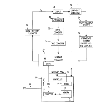
FIGURE 1 illu~ ~es a prior-art digital/RF system 10. The RF system 10
O~lat~3 to convert fligj~i7~d voice andlor data, as may be supplied from a land-based
c~w~lk (not shown), into an RF signal for trAn~mi~ion to â wil~,le3s l~ AI (not
shown). The system 10 also o~t. s to receive RF signals and to convert such
signals into ~ligi~i7~1 voice and/or data signals for ~ A;on back to the land-
2s based network.
The digital/RF system 10 co~ .. ;~s a controller 14, in~ fling a
miclo~ cessor 16 and ~A~soei~t~ memory 18, for controlling the system and for
;..ful...A~;on along an I/O line 19. ln particular, the c ontroller 14
controls the operation of a base-band processor 20 (e.g., a digital signal processor or
30 group of such processors) that functions to process incQ~ing voice and/or data
2156655
signals (h~ f~l~,d to as "fol..~d signals") that are supplied to the
controller from the land-based ~ lw~lh~
The base-band ~ ce~r 20 sl~pliPs the now~ sse~l fo~..~d signals to an
RF !. ..,~i,,,;lt. . 24 that is controlled by the controller 14. The ~ .,..lt~ ~ 24
5 m~l~ tes the l~ioc~ ese~1 forward signals from the base-band yl~ssor 20 on a
~,f~.lce carrier signal to g~.~ an RF signal ~lepi~t~l by the legend T~ The RF
signal Tx is supplied to a duplexer 26 that sep ~nteS the 1~ and receive signal
paths.
The d~l~ ~ 26 couples ~~;~,d signals ~om the A.~f ~ A 30 to an RF
o lece;~,. 34. The l~;~v 34 ~ S the RF signals from the ~..t. .~A to yield an T.~ P-l;qt~ Frequency (IF) signal. A comhinPA IF ,~ei~,. and A/D CG,
36 con~,.ls the IF signal from the r~ . 34 into a base-band signal (1~
,~ f~ d to as a "1~ signal) that is ~u~l;ed to the base-band processor 20 for
proce~i~ The base-band plocessor 20 plOCei;~S the reverse signal from the
5 col~illed IF l~;~_. and A/D coll~_.t~r 36.
In the past, the digital Plf~ lt~; (i.e., the controller 14 and the base-band
.,ocejsor 20) were tested se~ t~ly from the RF elemf nt~ (the t.~ .";l~l 24, thereceiver 34, and the IF ,~;~_. and A/D converter 36). Such s~&ale testing has
proven il~con~ L To o~ on,e this difficulty, an improved digital/RF system
20 10', shown in FIG. 2, has been developed to fi~'ilit~tf unified testing. The RF test
system 10' of FIG. 2 il~cllldcs ~llf ..f ~ in common with the test system 10 of FIG. 1,
and, th_.e~l~, like l~ f~ mlml~ have been employed in FlG. 2 to describe like
f k -~f -~ Ithongh not shown in FIG. 2, the digital/RF system also includes the
duplexer 26 and Al~t~ A 30 of FIG. 1.)
The controller 14 ofthe digital RF system 10' of FIG. 2, like the controller 14
of FIG. 1, i~ i~ a lll~ /18 ~at stores control co.. ~ However, unlike ~e
memory 18 of FIG. 1, the ~ ,mGI~ 18 of FIG. 2 has a portion 38 dedicated to storing
test p~ for testing the RF ~ tl - 24, the RF r~;~_. 34 and the IF l~i~
and A/D ~ll~e.t~ 36. Although the controller 14 has been illustrated as cQ~ g
30 a single memory 18 that stores both control comm~n~ls ~ well ~ test p~lt~ fortesting the RF el~o-nn~.nt~, a se~al~ memory could be provided for storing such test
~ s 2156655
e In nd~litil~n~ a large mass storage device, such as a m~etic disk drive (not
shown), could be s~ le~ for the memory portion 38 to supply the test ~I~ e
via the IIO line 19.
The controller 14 of the test system 10' of FIG. 2 also differs from the
s controller 14 of FIG. 1 in another regard. As seen in FIG. 2, the controller 14 of the
test system 10' ;~ a Ro~ Scan Master circuit (BSM) 42, typically in the
form of an AT&T modd 497 AA Bouild&~-Scan Msster circuit, available from
AT&T Mic~oele~ onics, Alle~ ., Pe~ ia The BSM 42 COO~:~ateS with
the ~ ,o~ c~sol 16 of the system 10' to carry out Boundary-Scsn testing of the
lo digital c~ t~ (not shown) within the controller 14 other than the mi~oplocessor
16 and to carry out Boul~ -Scan testing of the base-band plocessol 20. To that
end, the base-band ploc~ssor 20 is configured with a Boundary-Scan &cl.;t~
In M~liti~n to the BSM master 42, the controller 14 of FIG. 2 in~ es a
bridge 44 coupled to the BSM via a bus 46. The bridge 44 filnl~tion~ to distribute
lS Boundary-Scan test signals g~ ~ on the bus 46 by the BSM 42 to the digital
el~ -.. 1-; in the controller 14 that are to be Boundary-Scan tested by the BSM. A
bridge 48, i~l..nti.~l to the bridge 44, is provided within the base-band lnoccssor 20
and serves to distribute Buulld~ -Scan test signals within the base-band ~i~ocessol
that are ~ A thereto via the bus 46. Both bridges 44 and 48 typically each
20 co...l.. ;~ an Addr~ss~le Sh~dow Port (ASP) m~mlf~r,tnred by Texas Inst~ s ora Scan Bridge device ... ~..r;..~ d by National Sernicon~ ctor Col~l~ion.
R~f~Ti~ to FIG. 2, to ~r~...plixh int~ teA testing of the RF cl~ (i.e.,
the RF !.~ 24, the RF l~ei~ 34, and the IF ro~i~ and A/D coll~,.h,. 36),
the system 10' i~el~d~s a coupler 49 for c~ the RF ~ ., signal Tx to an
~ tor 50. The attenuator 50 ~(h ~ t~,s the signal l~ei~,~ from the coul,ler 49 to
yield a l~uced sh~ lh signal for input to a down~onverter 52. The down-
converter 52 down~ll~,.ls the ~h -~ t~ x...;ll~.. signal Tx to a lower frequencysigral for input to an analog-to-digital (A/D) conve.t~,t 54. The A/D con~,~,.t~,. 54
converts the analog signal produced by the down-co.,~t~. 54 into a digital signal
30 for input to the base-band processor 20.
6 215665~
The coupler 49 not only couples t-he RF ~ . signal Tx to the ~tt. ~ t~l
50, but also couples the signal to a loop-back com~e~tion 56 that feeds the Tx signal
to the RF l~;-~ 34. In this way, the Tx signal p,oduced by the RF l.~ t~ 24
is i,ul~pli~d to the RF l~;~_. 34 for ~l.om~lnl~tion As described previously, the
5 ~1.~ ll~l..l~.t d sign~l p~ l~d by the RF rc~ . 34 is input to t~he IF ~ and
A/D C~ .t~. 36 that CO~ .tS the RF lC~;~. 34 signal into a digital signal input to
the base-band pn)cessor 20.
Overall testing ofthe digital/RF system 10' is calTied out in the following
m~nnf.r First, the digital ~lc ~ within the controller 14 (other than the
10 rnicloplocessol 16) are sllu;tu~ y tested via BOul,da~ Scan testing, as is the base-
band plOCGSSOl 20. As clesrribefl, such testing is carried out via the BSM 42. For a
more col,~ t~ d~. ;l.tion of Boulld~-Scan testing"ef~ ce should be made to
the afol~ tioned IEEE l~ul~ tion, herein n~COI~Oldt~i by ~. f~ ce. In ~d-liti~n
to ~r~co.. .plichir~ testing of the digital ele~ ; within the controller 14, the BSM 42
may f~-'ilit~t~ Boulld&.~-Scan testing of mixed signal el~ within the system that
are testable by the BOul,dal ~-Scan test technique.
Once structural testing of the digital portion of the system 10' has been
carried out via the Bo~ld~y-Scan test technique, then the RF elc~,le.,~ are tested.
The RF t~r~mitter 24 is tested via the base-band processor 20 by first down-loading
test p~t~- -- ~-~ from the IlRn10l,~' portion 38 to the base-band processor 20. The test
are then applied to the RF ll .~i...;lt. ~ 26. In acco,~ce with the down-
loaded test p ~ , the RF l~ 24 produces the RF signal Tx . The RF
signal Tx is attenuated by the at~udto, 50 and then down~onverted by the down-
co~.t~. 52 before being tli~iti7~1 by the A/D con~_~. 54. The f1igiti7~d signal
25 produced by the A/D COll~,_.tl,. 54 iS then ploces~d by the base-band processor 20 to
det~ o. ~e operability of ~e l-~ t~l 24.
The RF receiver 34 is tested in a similar fashion. The RF signal Tx g~l1e.,lled
by the ~ ...;lt~ 24 in l. ~on~e to each applied test pattern is coupled to the RF
~ei~. 34 via the loop-back co~ ion 56. The Tx signal received by the RF
30 receiver 34 is demo~llll~te~ thereby to yield an IF signal that is down-converted and
~1igiti~ by the IF ~ and AtD converter 36 to yield a base-band signal. This
7 - 2156655
base-band signal is plocess~d by the base-band p~ 20 to ~et~ .F. the
op~ ility ofthe RF l~;~r 34 and IF fCCe;~" and A/D COIl~ ~t~" 36.
As may be appreciat~d, the digital/RF system 10' fi~ilit~lt~S testing in an
integrated manner since both the digital portion and the RF portion are tested via the
5 controller 14 wi~,~ul the need for sepa~e test eq ~ P-
~
It is to bc ....~ J~ ~atthe above~-~ibed ~.m~;..u ~ ; are merely
ill..,h,.t;~_ ofthe principles of the invention. Various modifications and cL~ ges
may be made thereto by those skilled in the art which will embody the p . ;.~ ,les of
the invenffon and fall within the spirit and scope thereof.