Note: Descriptions are shown in the official language in which they were submitted.
WO94/19736 -l- PCT~S94/02091
TITLE: pO~ART.~ WORK STATION AND DATA
COLLECTION T~R~TNAT. INCLUDING
SWIT~ART~ MULTI - PURPOSE TOUCH
SCREEN DISPLAY
CRO88 RBF~r'~ TO RELA~ED APPLICATION8
(Claiming Benefit Under 35 U.8.C. 120)
10This application is a continuation-in-part of
co-p~n~;n~ application U.S. Serial No. 08/048,873,
filed April 16, 1993, which is a continuation of
application U.S. Serial No. 07/948,034, filed
September 21, 1992, by Phillip Miller et al.,
15which is a continuation of U.S. Serial No.
SUBSlTrUTE SHEET (RULE 26~
WO94/19736 2~57~ 2- PCT~S94/~2091
07/347,602, filed May 3, 1989, by Phillip Miller
et al., now abandoned, and a continuation-in-part
of co-pending application U.S. Serial No.
08/023,840, filed February 26, 1993, by Arvin D.
Danielson, Darrell L. Boatwright, Darald R.
Schultz, Rickey G. Austin, and Dennis Silva, which
is a continuation-in-part of U.S. Serial No.
07/728,667, filed July 11, 1991, by Arvin D.
Danielson, Darrell L. Boatwright and Darald R.
Schultz.
Reference is also made to the following
related application U.S. Serial No. 08/005,324,
filed January 15, 1993, by George E. ~hA~ Jr.
et al-, which is a continuation of U.S. Serial No.
07/549,298, filed July 5, 1990, now U.S. Patent
No. 5,180,232, which is a continuation-in-part of
U.S. Serial No. 07/216,868, filed July 8, 1988,
now U.S. Patent Des.315,573, and a
continuation-in-part of U.S. Serial No.
07/227,195, filed August 2, 1988, now abandoned,
and a continuation-in-part of U.S. Serial
No. 07/347,602, filed May 3, 1989, now abandoned,
which is a continuation-in-part of U.S. Serial No.
07/346,771, filed May 2, 1989, now abandoned.
SUBSmUTE SHEET (RULE 263
2157~39
WO94/19736 PCT~S94/02091
BACKGROUND OF THE INVENTION
The invention relates generally to data
collection and processing systems and to portable
data terminals thereof. In particular, the
invention relates to data input and output
5 arrangements and to data display and verification.
Portable data terri~A 1~ are well known
components of state of the art business systems.
The data terminals may be taken to merch~n~;se
storage facilities for inventory control or
customer service transactions, or may be used in
any one of various other commercial applications
to serve as data input or output devices for
central data processing and control stations.
It appears that operations and usefl~lnecc of
such central data processing or control stations
are enhanced with efficient and prompt data entry
and retrieval at the working level. Most
efficiently data entry and retrieval may be
obt~;ne~ through a plurality of portable data
terminals which selectively become coupled to the
central processing or control stations. Operator
controlled data interchange may be established
between central stations and the portable data
terminals.
Increased versatility in data input and
output arrangements tends to increase power usage
of the portable data terminals, thereby decreasing
usage periods between battery ~Y~hAnges or
recharging operations. Touch sensitive or pen
actuated data input systems are known. Use of pen
actuated data entry systems in hand held, portable
data terminals has been limited in the past in
part because of power management limitations,
partly because of problems relating system
compactness, and also partly because of problems
relating to terminal limitations when an otherwise
practical pen-type data entry is provided as a
SUBSIITUTE SHEET (F ULE 26~
WO94/19736 PCT~S94/02091
~ S~39
sole or main d~ta acquisition mode for a portable
data terminal.
SU~ SHEET (RULE 26
WO94/19736 ~1~ 7 0 3 9 PCT~S94/02091
SU~MA~Y OF THE lNv~ ON
It is therefore an object of the invention to
provide an improved data input and display with
increased functionality.
It is another object of the invention to
arrange an alphanumeric keyboard for multi
orientational use.
Further in accordance herewith it is an
object of the invention to provide a pen-activated
data input device which interactively may be
prompted through display screen prompts.
Another object of the invention is to provide
a robust data terminal having a display screen
sized to permit operator input via pen strokes and
having the capability to change to keyboard
entries interchangeably with entry via pen-type
signals.
Yet another object of the invention is a
power management control function implemented
through software controlled microprocessor
functions, the power management function including
selectively shutting the data terminal down
without loss of current data interchange status
states on an Input-Output bus (I/O Bus).
According one aspect of the invention, it is
consequently contemplated to increase the data
input capacity of a portable data terminal with a
touch sensitive liquid crystal display which
functions as an exten~ keyboard and as a
provision for entering graphic data such as
signatures. Another keyboard may be a numerical
keyboard or may be activated as a function
keyboard to supplement a touch sensitive keyboard
implemented as an overlay of a display screen.
In an embodiment in accordance with the
invention, keys of the touch sensitive keyboard of
the display screen of the portable data terminal
are selectively re-orientable with respect to the
SUBSml.~ SHEET (RULE 26~
WO94/19736 PCT~S94/02091
~ 9 -6-
data terminal. In accordance with a particular
feature of the invention, the keys or key areas of
the touch sensitive keyboard are reoriented by
switching key assignment areas within the touch
sensitive display screen and by reorienting
indicia within each of the switched touch
sensitive areas of the board to change the
orientation of the indicia to ~correspond to a
change orientation of the keyboard of the touch
sensitive area.
Further in accordance with the invention, a
keyboard is disposed adjacent a display screen of
a portable data terminal in a frontal face of the
data terminal. The keyboard includes an array of
keys, each key having an assigned function, and an
array of indicia identifying the function of each
of the keys of the array. The array of indicia is
disposed on a matrix removably attachable to the
frontal face of the data terminal. The array of
indicia may be removed and replaced by another
array of indicia, showing reassigned functions of
each of the keys, and the functions of the
respective keys are reassigned in accordance with
such other array of indicia.
In a particular embodiment of the invention,
the array of indicia is displayed on a sheet of
material which may be attached as an overlay to
the area of the keyboard in one of at least two
distinct orientations, and the assignment of the
functions of the keys may be switched to
correspond to a reorientation of the switched
sheet of indicia.
Also according to the present invention, a
data terminal has a display screen and graphic
data input surface coincident with and disposed
beneath the display screen. Data input into the
graphic data input surface is o~tained via an
electromagnetic pen.
3JBSmU~E S~lEEt (F~ULE 2st
~ WO94/19736 215 7 0 3 ~ PCT~S94/02091
Further in accordance herewith, the data
terminal includes operation shadowing circuits
which include a function of shadowing Input-Output
(I/O) device states and a function of storing
miuLu~ocessor register states during a shutdown
proce~lre. Pursuant to the shadowing and
mi~Lo~ocessor register storage, the data terminal
may be shut down and re-activated without loss of
control or I/O status data and with the ability to
complete an operation in progress during the time
of shutdown of the data terminal.
Further in accordance herewith, a data
terminal includes a shock and weather resistant
housing and a keyboard orientation with respect to
a display screen which causes an included angle to
protect both the keyboard and the display screen
from contact with a flat hard bottom surface
during a fall of the data t~rminal against such
surface. Co-molding of shock absorbing material
to the surface of the housing distributes impact
forces to which the data terminal may be exposed
as a result of a fall. Co-molded sealing strip
disposed on access covers provide a weather-sealed
housing while further enhancing impact resistance
of the data terminal.
A removable base plate includes a co-molded
weather seal which also provides impact
resistance. A particular base plate or base
includes an accessory pod which is centrally
disposed along a central axis of a housing of the
data terminal. The acc~ory pod has a width
transverse to the longit~l~; n~ 1 axis which is less
than the transverse width of the data terminal,
the accDC~ory pod including a hAn~qrip portion by
which an operator may hold the data terminal while
operating the data terminal.
The base is exchangeable for any of a number
of other bases, each base having a particular one
SU~UTE SHEET (RULE 263
WO94/19736 ~3~ -8- PCT~S94/02091
of a number of desirable accessory features. At
least one of the bases is contemplated to include
a ~cAnn~r for reading indicia which may be
disposed on a surface external and separate from
the data terminal. The sc~nner may, for example,
be a bar code scanner. The data terminal may
feature two hand strap provisions disposed
externally of the housing. An operator may insert
fingers or a portion of the hand between the
housing and one of the handstrap provisions to
retain the unit by friction between the hand and
the strap.
Various other features and advantages of the
invention will become apparent when the detailed
description below is read in reference to the
appended drawings.
SUBS~E StlEET (RULE 26
21~ 7~39
WO94/19736 PCT~S94/02091
B~T~ DESCRIPTION OF THE DRAWINGS
The detailed description refers numerically
to elements of the drawings wherein:
FIG. l is a frontal view of a data terminal
showing a touch sensitive display screen in
combination with a keyboard in accordance with an
embodiment of the present invention;
FIG. 2 is a schematic frontal view of the
data terminal of FIG. l showing a preferred
overlay for a keyboard of the data terminal;
FIG. 3 is a similar schematic frontal view as
in FIG. 2, with the overlay shown in a reoriented
position with respect to the position of that
shown in FIG. 2 relative to the data terminal;
FIG. 4 shows yet a further orientation of the
keyboard and the overlay which may be desired in
accordance with the invention; and
FIG. 5 shows a further orientation of the
keyboard and overlay in accordance with the
invention;
FIG. 6 is a side view of the data terminal
shown in an upright position as in FIG. l and
showing frontal and rear shells of a housing of
the data terminal;
FIG. 7 is a simplified schematic diagram of
the data terminal showing basic functional
elements of the data terminal in FIG. l;
FIG. 8 is a frontal view of the data terminal
shown in FIG. l, and further modified with a
sc~nnPr module, such as a laser -ecAnner module for
reading bar codes;
FIG. 9 is a frontal view of the data terminal
shown in FIG. l, showing in an alternative
embodiment an attachable grip portion attAç~e~ to
a lowermost end of the longi~ ;nAl housing of the
data terminal;
SUBSml.~ SHEET (RULE 26
W094/19736 ~ PCT~S94/02091
--10--
FIGS. lO and 11 depict tab positions of a
keyboard template structure as an alternative to
the structure shown in FIG. 2;
FIG. 12 is a simplified representation of a
data terminal system including a data input screen
and keyboard combination in accordance with the
invention;
FIG. 13 is a pictorial representation of the
data terminal shown in FIG. 12 showing an
accessory pod of the data terminal;
FIG. 14 is a sequence chart of an assembly
process in accordance herewith;
FIGS. 15 and 16 illustrate features involved
in a co-molding process;
FIG. 17 shows details of a battery
compartment access door;
FIG. 18 is a diagram of electronic functions
of one emho~;ment of the data terminal in
accordance with the invention;
FIG. 19 is a diagram of electronic functions
of a modified embodiment of the data terminal
showing further details in accordance with the
invention;
FIG. 20 is a diagram of electronic functions
of an input-ouL~uL function board which may be
coupled to an input-output function connector
shown in FIG. 19, for example;
FIG. 21 is a control logic flow diagram of a
sequence that be followed during power up or power
down operations of a data terminal according to
the invention;
FIGS. 22, 23 and 24 show schematically
simplified an end view, a top view of an upper
end, and a cut through the upper end of a
modification of a data terminal shown in FIG. 12;
FIG. 25 is a pictorial representation of the
data terminal, showing a frontal face thereof;
~ SHE~ ~ULE ~3
~ WO94/19736 21~ 7 0 3 9 PCT~S94/02091
FIG. 26 is a partial bottom view of the data
terminal shown in FIG. 25;
FIG. 27 is a diagram of electronic functions
of the data terminal shown in FIGS. 12, 13 and 25,
showing preferred modifications that may be made
within the scope of the invention over the
functions described with respect to FIG. 19; and
FIG. 28 is a diagram showing contemplated
functions which may be executed by a
communications interface circuit shown in
FIGS. 18, 19 and 27.
SUBSlTrUTE SHEET (RULE 26
W094/19736 3~ -12- PCT~S94/02091
DETA~T~D DESCRIPTION OF THE INVENTION
In reference to FIG. l, there is shown a
frontal view of a portable data collection
terminal or data terminal which is designated
generally by the numeral l0. The data collection
terminal lO is a hand-held, portable unit, which
is understood in the art as being powered by a
self-contained power source. Such a portable data
terminal lO may operate in what is ~eferred to as
a batch mode in which data are coIlected by ànd
stored within the data terminal lO to be
transferred to an alternate data processing unit
or host computer (not shown) in a comprehensive
"batch" type operation. In the alternative, the
data terminal l0 may be in communication with such
a host computer in an interactive or on-line mode
via a data communications link, such as a radio
frequency tr~ncc~;ver arrangement. The presence
of such a radio transceiver is indicated as an
alternative embo~iment by a radio antenna ll,
shown in phantom lines as the only externally
visible element of such a transceiver- An
elongate housing 12 preferably of a
high-impact-strength plastic material encases the
data terminal lO. Various types of materials are
known and are commercially available.
The housing 12 of the data terminal l0
features a front surface 14. A display screen 15
is attached to the front surface 14 and may occupy
a major portion of such front surface. A keyboard
16 is disposed adjacent the display screen 15.
The display screen 15 is desirably a liquid
crystal display screen ("LCD æcreen"). State of
the art LCD screens generally employ "double super
twist" technology which has been found to provide
satisfactory viewing contrast under most direct
lighting conditions. It is further possible to
provide backlighting for LCD screens. However,
SUBSmUTE SHEET (RULE 26~
~ WO94/19736 PCT~S94/02091
21S7039 '
-13-
power considerations may require se~ective
disablement or even deletion of backlighting. As
is apparent from FIG. 1, with respect to the
housing 12, the LCD screen 15 is of a
comparatively large size, a lateral overall width
of the LCD screen 15 ext~n~;ng over general
lateral boundaries 17 and 18 of the elongate shape
of the housing 12. The longitl~;nAl extent of the
display screen also occupies a major portion of
the front surface 14 of the data terminal lO. The
keyboard 16, being limited in size by the
available area on the front surface 14,
co~-c~quently, would function primarily as a
"numerical" keyboard, such as for numeric data
entry.
An active display area 19 of the display
screen 15 may be of a preferred minimum area of
approximately 80 X 120 millimeters. The active
area 19 i8 preferably a "bit-mapped" display,
me~n; n~ that the display is comprised of an array
or matrix of individually addressable display
elements 21, and each such element or pixel 21, a
representative location of which being referenced
in FIG. 1, is driven by a data state of a
particular individually addressable location in a
memory 22 (shown schematically in FIG. 6) of the
data terminal lO. It is further found desirable
that memory locations which control the activation
of respective ones of the pixels 21 of the display
screen 15 enComrAcc more than single memory cells,
such that more than a simple on-off function, but
rather a gray scale value may stored in each
dedicated group of cells of the memory 22 to be
applied to the particularly addressed pixel 21.
Because of the electrical connections for
implementing the display screen functions, the
display screen 15 includes a boundary area 31
which extends beyond the lateral confines of the
SUI~UTE SH~Er (F ULE 263
WO~4/19736 25~0~ -14- PCT~594102091
housing 12 of the data terminal 10. Because of
the desirably large active screen area 19, for the
display information compatible with that on a
st~n~rd computer screen, for example, the minimum
desirable size of the display screen 15 tends to
conflict with a design intent to maintain an
overall size of the data terminal 10 as small as
possible. In that the enlarged screen area of the
data terminal 10 occupies a substantial part of
the front surface 14 of the housing 12, the front
surface 14 seemingly lacks the frontal surface
area to accommodate both the numeric keyboard 16
and an alphabetical keyboard in addition to the
display screen 15.
In overcoming space restraints on the front
surface 14, the display screen 15 is ideally
provided with a touch sensitive active surface
area 32 as an overlay to the LCD screen for use as
a keyboard. The touch sensitive active surface
area 32 may be implemented in a currently
preferred embodiment by known t~h~ologies which
employ, for example, either capacitive or
resistive swit~h ~ ~ and sampling ter~n; ques to
determine coordinates of a point on the surface
area 32 against which a contact pressure is
exerted. The overlay area 32 is essentially
transparent, such that information displayed on
the screen 15 remains clearly ~isc~rnible. For
example, the touch sensitive active area 32 may
selectively be configured as a keyboard for manual
input of alph~h~tical characters. In the
preferred embodiment the size of the touch
sensitive overlay area 32 corresponds to active
display area 19 of the LCD screen 15. It should
be noted, however, that such choice is one of
convenience, and that less than the active display
area 19 of the display screen 15 may be
encompassed by the touch sensitive active area 32.
SU~ITU~E SHEET (RULE 26~
21S7039
WO94/lg7~ PCT~S94/02091
-15-
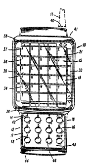
A keyboard array 34 of active key areas 36
may be displayed on the display screen 15 to
correspond to the assigned key areas 36. Each of
the key areas forms a discrete functional unit, in
S that a touch or pressure in any or all portions of
such discrete area 36 results in one and the same
input signal being generated. Indicia 37 of
letters or of control functions also may be
displayed directly beneath the respective active
key areas 36 of the array 34 on the screen 15.
The indicia 37 correspond to and identify input
signals generated in response to contacts being
made in such designated key areas 36. The display
of the keyboard array 34 and of the indicia 37 is
desirably selectively activated whenever keyboard
entries are to be made via the touch sensitive key
areas 36. Also, it may be desired to alternate
between a display of data as feedback of data
entered and the display of the keyboard array 36.
In a further variation of the described embodiment
it is contemplated to deactivate the touch
sensitive active area during periods in which the
display screen 15 is used entirely for data
display. Another advantage of the bit-mapped
display screen 15 and the correspondingly
identifiable touch sensitive area 32 is that
graphic data displaying a customer invoice may
have a designated area, selectively activated, for
receiving a signature as acknowledgement by a
customer. The signature is stored in memory and
may be recalled and reproduced on paper copies of
the invoice by a central processing station. If
all other areas displaying invoice information are
deactivated, so as not to receive a touch
sensitive input, no changes can be made at the
time the acknowledgement is requested. The use of
alphanumerical data collection is further advanced
by character recognition algorithms for processing
SUBSlTrUlE SHEET (FWLE 263
WO94/19736 ~ ~ 7 ~ 3 9 PCT~S94/02091
-16-
and storing actual data in response to
hand-produced inputs to the screen. For example,
the display may provide line spacings as guides
for receiving written characters. Within such
designated boundaries a sensed pattern of graphic
inputs is compared to a character of information.
The apparently matching character is displayed.
The display is an immediate feedback as to whether
the correct character has been recognized. If an
incorrect character appears, a graphic correction
is made as a deviation with respect to the
displayed character. Various other advantages
will appear from the further description of the
preferred embodiment of the invention .
Touch sensitive screens require electrical
couplings to be made along horizontal and vertical
peripheral borders 38 and 39 of the display screen
15. Such electrical couplings are space consuming
and need to be made in addition to bit-mapped
display screen co~nPctions, which are also made
along the peripheral borders 38 and 39. All of
such connection regions constitute inactive areas
of the screen 15. Preferably, to make optimum use
of inactive horizontal and vertical connection
areas adjacent the active area of the display
screen 15 are used for displaying permanently
imprinted information, such as grid indicators 40
and cursor indicators 41. The peripherally
displayed information helps in delineating the
keyboard area 34 with respect to the display
screen 15. In further reference to FIG. 1, the
active area 19 of the display screen 15 desirably
is of elongate configuration, thereby minimizing
the lateral projection of the display screen 15
beyond the lateral boundaries 17 and 18 of the
housing 12. However, because of size of the
display screen being greater in the vertical
direction of the data terminal lO, it appears
SUBSmUTE SHEET (RULE 26~
~ WO94/19736 21 S 7 0 3 9 PCT~S94/02091
desirable to display long lines of data in the
longitudinal direction of the screen, hence
perpendicular to the direction in which data might
normally be displayed on the screen 15.
Adjacent the display screen 15, the remaining
portion of the front surface 14 of the data
terminal lO is occupied by the numerical
keyboard 16. According to a preferred embodiment
of the invention, indicia 42 identifying the
numerals or functions of the numerical keyboard 16
are disposed on a template 43. The template 43 is
a flat sheet of material which features a
plurality of apertures 44 to correspond in size
and location to the size and location of keys 46
arranged in a preferred "3 X 4" array 47. The
template 43 consequently fits over the keys 46 and
rests when attached to the keyboard 16 adjacent
and in contact with a base surface 48 of the
keyboard 16. In the example of the keyboard 16
shown in FIG. l the keys 46 ~L G L~de through the
base surface 48 and similarly through the
template 43. As shown the keys 46 are circular in
their plan view. It should be understood that
keys of other shapes, for example, square keys or
even rectangular keys may arranged as the circular
keys 46 and marked with indicia disposed on the
template 43 as described herein.
The template 43 is preferably removably
attached to the base surface 48 which may be part
of the front surface 14 of the housing 12.
Consistent with a desirable alternate orientation
for displaying data characters in lines on the
display screen 15 longit~ A lly with respect to
the data terminal lO, it appears to be
advantageous to reorient the indicia 42 on the
template 43 with respect to the data terminal lO
when information displayed on the screen becomes
reoriented with respect to the data terminal.
SU~SllTUTE SHEET (RULE 26~
WO94/19736 2 ~ 5 7 ~ 3 ~ PCT~S94/02091 ~
-18-
FIGS. 2 through 5 show in a simplified
representation of the data terminal 10 various
orientations of the template 43 with a
correspondingly physical reorientation of the
indicia and alternate orientations of the keyboard
16. In FIG. 2, the template 43 is shown in a
first position, in which the indicia 42 disposed
on a first major surface 49 of the template 43 are
oriented to be read when the data terminal is
operated with the keyboard 16 disposed below the
display screen 15 or more closely disposed toward
an operator than the screen 15 when the data
terminal 10 is held by the operator in a common
operating position. In such a position, lines 50
of data would be displayed on the screen 15 in a
left-to-right position across the width of the
data terminal 10, or in parallel with, hence,
non-intersecting with the keyboard 16.
In FIG. 3, a second set of indicia 51 is
displayed on a second major surface 52 or flip
side of the template 43, the template 43 being
thus reversible and having been reversed. On the
~e~on~ major surface 52, the ~?con~ set of indicia
51 is oriented to identify the functions of the
keys 46 at right angles to the orientation of the
original set of indicia 42. Thus, data displayed
on the display screen 15 correcpon~ngly would be
shifted by ninety degrees from their original
orientation on the display screen 15, allowing a
longit~ display line 54 and, hence,
permitting more characters in each line 54 of
display. The correspo~ingly reoriented set of
indicia 51 on the template 43 permits the keyboard
16 to be read by an operator reading data on the
screen 15 without a need for the operator to
transpose numbers or functions being shown on the
template 43. This latter orientation of the
displayed data and the set of indicia 51 is
SUBSlTrUTE SHEET (RULE 263
WO94~19736 21 S 7 0 3 9 PCT~S94/02091
--ls--
mutually coextensive, such that line extensions of
the displayed data would intersect the keyboard
16.
In reference to both FIGS. 2 and 3, by
transposing the orientation of the keyboard 16, a
numerical assignment of at least a major pattern
of the keys 46 iS preferably also transposed to
maintain keystroke patterns to which operators of
the data terminal 10 may be accustomed. In a
preferred ~hoA; ment a reassignment of the
functions of the keys 46 would be performed
simultaneously with a reassignment of functions of
the key areas 3 6 of the touch sensitive keyboard
array 3 4 and with a reorientation of the display
on the display screen 15. FIGS. 2 and 3 are shown
with both lines 50 and 54 of data in part of the
display screen 15, and with keyboard areas 36 in
another part of the screen 15 to illustrate the
simultaneous reorientation of the data display and
20 the keyboard array 34 and its assigned touch
sensitive key areas 3 6.
The change in orientation of the display and
the corresponding reassignment of the keys 46 and
key areas 3 6 may be originated by operating a
25 switch, by a keystroke operation of one or a
combination of the keys 46 or of one or a
combination of the key areas 36 which define the
keyboard array 34 of the touch sensitive screen
32. It is to be realized that orienting the
template 43 iS, in the described embodiment, a
physical function that would be performed by an
operator of the data terminal 10. A simplifying
step seeks to combine the physical reorientation
of the template 43 with functional switching or
reorientation of the keys 46, the key areas 36 and
the display screen 15.
Accordingly, the template 4 3 may be adapted
to become attached to the front surface 14 of the
SUBSIT~ SHEET (RULE 26t
WO94tl9736 PCT~S94/02091
215~ ~3~
-20-
data terminal lO in a reoriented position and
simultaneously therewith a reorientation of the
display screen 15 and the touch sensitive keyboard
array 34 may be initiated. FIG. 2 shows a
plurality of peripheral tabs 61, 62, 63, 64 and
65. The positions of the tabs 61 through 65 along
respective edges 66, 67, 68 and 69 of the template
43 correspond generally to positions of
representative sensors 70 and 71 disposed in
reCDC~es 72 and 73, for example, of six
representative peripheral recesses 72 through 77
for retAini~q the template 43. The tabs
consequently serve a dual function of physically
seating the template 43 in its position, and of
selectively engaging or activating one or more the
C~cors 70 and 71, such that by such selective
activation the orientation of the template 43 is
determined by the data terminal lO. The sensors
70 and 71 and the receCcDR to receive the tabs may
be disposed in housing ridges 78, 79, 80 and 81
disposed peripherally about the keyboard 16. The
sensors 70 and 71 may be electrical sensors of a
direct contact type, such as electrically
conductive pads which may be bridged by
electrically conductive strips disposed on the
template 43. Typical bounce suppression circuits
may be used to eliminate false signals due to
contact bounce and establish a reliable, switched
electrical co~nection when predetermined ones of
the contact pads of the sensors 70 and 71 are
bridged upon attachment of the template 43 to the
front surface 14 with a selected orientation. As
another alternative D~ho~;ment, the sensors 70 and
71 may be magnetic sensors.
In a described, currently preferred
embodiment, instead of being magnetic type sensors
or electrical contacts, the sensors 70 and 71 are
described as being photoelectric sensing cells.
SU~IU~ SHEET (RULE 26~
~ 094/19736 21 S 7 0 3 9 PCT~S94/02091
When the tabs 61-65 are inserted into respective
r~ces~^-, photoelectric sensing by the ~nCors 70
and 71 would be selectively affected in accordance
- with the orientation of the template 43. In
reference to FIG. 11, a selected area on an upper
underside 95 of a respective recess may be
reflectively coated to redirect light from a
source 96, such as a light emitting diode,
disposed adjacent an optical ~e~or 97, such as a
photo sensitive diode. When the template 43 is
attached to the keyboard 16 with an orientation in
which a respective one of the tabs interrupts the
light path between the light emitting diode 96 and
the photo diode 97, an appropriate orientation of
the template is recognized by a respective sensing
circuit lOO. The recogn;tion of the orientation
of the template 43 accordingly may be used to
reassign the key areas 36 of the keyboard array 34
and the keys 46 of the keyboard 16 as well as
reorient data shown on the display screen 15.
In further reference to FIGS. 2 through 5,
the simplified representations of the data
terminal lO show schematically indicated recesses
72 and 75 along the lateral boundary of the
housing 12. The tabs 61 and 62 are disposed
adjacent one another along the edge 66 and are
symmetrically disposed with respect to a center
point of the edge 66. The recesses 72 and 75 are
of equal length and are centered on the keyboard
16. The overall length of the adjacent tabs 61
and 62 including a gap 112 is the same as the
length of the single tab 64 on the opposite edge
68 of the template 43. The tab 64 is also
centered along its edge 68. Thus, whether the
~ 35 template 43 is rotated 180 degrees in a plane
parallel to the plane of the front surface 14, or
whether the template 43 is flipped over about an
axis 114 of rotation parallel to a longitll~;n~
SU~STrlU~ SHEET (RULE 263
WO94119736 PCT~S94/02091 -
2~7 ~3~ -22-
axis thro~gh the data terminal 1¢, the tabs 61 and
62 will be received by one of the recesses 72 or
75, while the single opposite tab 64 will be
received by the other recess 72 or 75.
In the described embodiment, in each of the
top and bottom ridges 79 and 81, respectively,
there are two recesses 73, 74 in the top ridge 79
and 76, 77 in the bottom ridge 81, respectively.
The recesses in each of the respective ridges 79
or 81 are symmetrically offset from the central
axis 114. The tabs 63 and 65 would be similarly
offset with respect to the central longit~ nAl
axis through the template 43 such that each of the
tabs 63, 65 occupy one of the rPc~cc~-c 73, 74, 76,
77, ~p~n~ on the orientation of the template
43. The sensor 71 is, for example, disposed in
the top recess 73. The ~ho~^n recess 73 is not
critical for the r~cognition of the orientation of
the template 43, in that any other one of the
r~C~^c 73, 74, 76 and 77 may be chosen to
achieve a desired reco~nition of the orientation
as described herein. Other changes in configuring
the template 43 with correspon~;ng changes in the
recesses are, of course also possible within the
scope of the invention.
For example, in reference to FIGS. 2, lO and
11, the tabs 63 and 65 of the template 43 may be
disposed across the central axis 114, yet somewhat
offset with respect thereto. As an example, a tab
121 is shown in FIG. 10, in which the tab 121 of
an alternately configured template 122, extends
into a single bottom (or top) recess 123. The
recess 123 is longer than the length of the
tab 121 by substantially one-half of the offset of
the tab 121 with respect to the centerline or
central axis 114. A sensor 124 is located at one
end of the recess 123. Thus, when the tab 121 is
inserted into the respective recess 123, the
SUBSllTU~ SHEET (RULE 28~
WO94/19736 215 7 ~ 3 9 PCT~S94/02091
-23-
sensor 124 will be covered when one major surface
of the template 122 is facing up, but will not be
affected when the template is flipped over about
the central axis 114. Of course, two
complementary tabs on opposite edges of the
template would be required comparably positioned
with identical offsets with respect to the central
axis 114 to obtain similar orientation indications
of the template as described with respect to FIGS.
2 through 5.
Referring again to FIGS. 2 through 5, it
should be noted that the sensors 70 and 71 have
unique combinations of binary states of being
unaffected or affected by an intervening one of
the tabs to distinguish betweer. the four different
desired orientations of the template 43. FIG. 2,
showing the data terminal lO in a "normal,
upright" position with the numerical keyboard 16
below the display screen 15 and the data lines 50
r~St~;nq across the width of the data terminal lO,
the sensor 70 is unaffected or normal, and the
sensor 71 is affected by the tab 63. It should be
noted that in the configuration of the template
43, the function of the tabs 61 and 62 is to
affect the retention of the template in the
respective recess 72 or 75.
In FIG. 2, the template has been flipped over
about a longitn~in~tl axis, such that its second
major surface 52 is expcsed. In this orientation
an operator would view the data terminal 10 with
the keyboard 16 toward the left. In such
orientation of the template 43, the sensor 70 is
affected by the tab 64. The sensor 71 is now
uncovered and unaffected by any of the tabs, in
that by flipping the template 43 over as described
the tab 63 which previously covered the sensor 71
has been transposed to occupy the tab position in
the symmetrically adjacent recess 74 (with respect
SUBSmUlE SHEET (RULE ~63
WO94119736 PCT~S94/02091 -
2~S~ ~3 ~ -24-
to the axis 114 as an axis of symmetry). It
should be noted that in this orientation of the
data terminal 10 the display screen 15 allows more
characters of information to be displayed in the
longer data lines 54. At the same time, the
numerical keyboard 16 and the alphabetical
keyboard array 34 are now laterally adjacent with
respect to each other. While such lateral
orientation permits more data to be displayed in
a single display line 54, the orientation is
distinct in that the numerical entry keyboard 16
would be more easily accessible by a left handed
operator than by a right hAn~P~ operator, while
the touch sensitive alphabetical keyboard array 34
as an overlay to the display screen 15 would be
more accessible to a right hAn~e~ operator than
the keyboard 16. Thus, in operational modes in
which the longitll~;n~l display lines 54 are
preferred, and depen~g on whether the numerical
or the ~lrh~h tical keys see more use, an operator
may prefer to have the keyboard 16 on the left
hand of the data terminal or on the right hand.
The latter mode, in which a longitll~ l data
display is oriented to place the keyboard 16 on
the right hand side as an operator would face the
data terminal lO, is shown in FIG. 4. The
orientation of the template in FIG. 4 is uniquely
identified by the states of the sensors 70 and 71.
The sensor 70 is unaffected being straddled by the
two tab~ 61 and 62, and the sensor 71 remains
uncovered in that the positions covered by the
tabs 63 and 65 are not affected by a 180 degree
rotation of the template 43 in a plane parallel to
the plane of the keyboard 16.
FIG. 5 shows a fourth arrangement of the
template 43 in accordance with the orientation of
which the indicia of the template are inverted
with respect to the normal or starting orientation
SU~SmUlE SHEET (RULE 26~
WO94/19736 215 70 3 9 PCT~S94/02091
-25-
of the indicia shown in FIG. 2. The orientation
of the template 43 as shown in FIG. 5 might be
used when the alphabetical keyboard array 34 is
favored over the numerical keyboard 16. Placing
the numerical keyboard 16 at the top of the data
terminal 10 decreases interference with the use of
the alphabetical keyboard array 34. In the
orientation of the template 43 as shown in FIG. 5,
both sensors 70 and 71 are activated, the sensors
70 and 71 indicating the presence of the tabs 64
and 65, respectively.
Since each of the four orientations of the
template 43 are associated with a particular
combination of states of the sensors 70 and 71,
the state of the senso~s is preferably used
correspon~ingly reorient the displayed data on the
screen 15. With respect to the above description
of the position of the tabs, it must be kept in
mind that the positions of the tabs of the
template 43 are of choice and are assigned for
illustrative purposes only. Thus, it may be
desirable to assign the positions of the tabs
shown in FIG. 4 to the orientation of the indicia
42 as shown in FIG. 2. The advantage of such
orientation is that if the orientation of the
indicia 42 in FIG. 2 is to be a default
orientation, then the removal of the template 43
would render the state of the activation of the
sensors 70 and 71 to be the same as the
orientation of the template 42 in such default
orientation. The arrangement of the tabs of the
template 43 as described above in detail might be
preferred when the longit~ nAl orientation of the
display shown in FIG. 4 is the default orientation
of displayed data. In a particularly contemplated
embodiment it may be preferred to place indicia,
oriented in accordance with the default
orientation, on the base surface 48 of the
~ SHE~ ~ULE ~3
WO94/19736 ~ PCT~S94/02091 -
-26-
keyboard 16 to identify the function of the keys
46 in their default orientation when the template
43 is removed from its place adjacent the base
surface 48.
S There are a number of contemplated electronic
switching modes by which the orientation of
displayed data on the display screen 15 may be
made to correspond to the orientation of the
indicia of the template 43. For example, it may
be desirable to normally retain the sensors 70 and
71 and any corresponding switch;nq circuits
inactive. Thus, unless activated, the sensors 70
and 71 and respective circuits would not place a
drain on the self con~inP~ power source of the
data terminal lO- In response to a simultaneous
depression of a combination of keys, for example,
the "l" and "3" key of the current orientation,
the sensors 70 and 7l may become activated for a
predetermined period of time. The time period
may, for example, be set to keep the ~ ors
active for three minutes. During the three-minute
period, the sensors may further be timed to
perform a predetermined number of "sample sensing
operations", such as one sample every ten or
fifteen seconds until the period of three minutes
has lapsed. At that time the selective sampling
would cease until the desired combination of the
keys 46 is again depressed. During such period of
activation, the orientation of the display of data
on the display screen and, of course, the
orientation of the indicia of the touch sensitive
keyboard array 34 would be switched in accordance
to the indication obtained by the sensors 70 and
71. For example, when the combination of the keys
"l" and "3" is held down simultaneously, a first
sampling by the activati~n of the sensors 70 and
71 may still indicate the same state of the
sensors as would be expected with the most recent
SUBSm~E S~IEET ~RULE 263
WO94/19736 21~ 7 0 3 9 PCT~S94/02091
-27-
orientation, in that the orientation of the
template 43 has at that time not been changed. A
second sampling by the sensors 70 and 71 may occur
- during the time when the template 43 has just been
removed. At that time neither of the sensors
would detect one of the tabs and the data display
of the display screen 15 is switched to the
default orientation, either as shown in FIG. 4, or
any other default condition as may have been
provided in accordance with the description
hereof. A third sampling by the sensors 70 and 71
may occur when the template 43 has been attached
to the keyboard 16 in its desired reoriented
position. The displayed data on the display
screen 15 would at this time shift to the new
orientation and the functions of the keys 46 of
the keyboard 16 would also be reassigned in
accordance with the new orientation. Provided the
template 43 is not reoriented further during the
remaining active sampling period, further samples
taken by the sensors 70 and 71 would simply retain
the present orientation until at the end of the
predetermined sampling period further sampling
ceases. However, while the sampling period is
still running, the template 43 may be switched
again to another orientation. The next following
sample of the orientation by the sensors 70 and 71
then again aligns the orientation of the data
display with the orientation of the template 43.
It should be understood, however, that the above
functional description of a means and method for
orienting the physical keyboard 16, the keyboard
array 34 and the display with respect to each
other is simply one example of implementing the
invention in accordance herewith.
In referenca to FIG 6, physical external
details of the data terminal lO are shown in a
side view thereof to illustrate particular
SUBSlTrUTE SHEET tRULE 26~
WO94/19736 PCT~S94/02091
Z~ 28-
handling features relative to the described
reorientation of the displays. In a preferred
emhoA;ment, the housing 12 of the data terminal lO
features a frontal shell 130 including the
described features of the display screen 15 and
the keyboard 16, and a rear shell 131. The rear ~ '
shell 131 desirably may correspond dimensionally
and functionally to the rear shell of a known and
currently available data terminal marketed by the
assignee of the present invention. It appears
that the features as will be described in greater
detail below of such currently existing housing
shell are of advantage in combination with the
present invention. The rear shell 131 includes a
grip portion 133 which is formed by a contoured
indentation 134 deviating from a generally
rectangular shape of the data terminal ~O. The
inwardly formed grip-conforming surfaces 135 of
the indentation 134 may in a preferred embodiment
be spAn~ by a hand strap 136, ends 137 and 138
of which being attached adjacent, respectively,
upper and lower ends 139 and 140 of the rear
housing shell 131. The grip-conforming surfaces
135 on each side of the rear housing shell 131
taper rearwardly toward each other to more readily
conform to a user's hand. The hand strap 136 is
in the preferred implementation of a width less
than the width of the data terminal lO.
Nevertheless, the hand strap 136 is of a width to
firmly retain the user's hand against the
contoured grip portion 133, even when the hand
grip momentarily becomes relaxed. The data
terminal lO is readily grasped and held with one
hand, either the left hand or the right hand of an
operator, allowing the other hand of the operator
the freedom to manipulate the keyboard 16 or the
keyboard array 34 on the front surface of the data
terminal. When the operator's hand is slipped
SUBSrrlLiTE SHEET (RULE 263
WO94/19736 ~1~ 7 0 3 9 PCT~S94/02091
-29-
between the hand strap 136 and the rear shell of
the housing the data terminal may be held in a
first or upright position, in which the lower end
140 of the data terminal lO is directed toward the
operator, while the upper end 139 faces away from
the operator. It is apparent, that the hand strap
is advantageously used to also hold the data
terminal lO in a second or lateral position at
substantially right angles to such an upright
position by turning the wrist of the hand that is
holding the data terminal lO. For example, a
person may be holding the data terminal by the
left hand in the upright position as shown in FIG.
2, for example. A twist of the wrist in a
counterclockwise direction p aces the data
terminal lO into a lateral position with respect
to the person holding the data termin~l, in which
a reoriented position of the indicia would
desirably correspond to that shown in FIG. 4. In
such reoriented lateral position, the keyboard 16
would be disposed on the right hand end as viewed
by the person holding the data terminal.
If a person would be holding the data
terminal lO by the right hand in the upright
position shown in FIG. 2, the natural twisting
motion permitted by the wrist would similarly
transpose the data terminal lO from such first
upright position to a second lateral position in
which the keyboard 16 would be disposed at the
left end of the data terrin~l. Such latter
reoriented position would ideally require a
reorientation of the indicia into the arrangement
shown in FIG. 3. Thus, a left handed person may
require a different lateral orientation of the
keyboard indicia and functions than a right handed
person. In contrast, the upright position is
accessible equally to both left and right handed
persons.
SUBSmUlE SHEET (RULE 26
WO 94/19736 PCT/US94/02091
30-
Further in reference to FIG. 6, the lower end
140 of the data terminal may typically be a
battery co~rArtment cont~i n; ng a power source 145
for electrically driving the functions of the data
5 terminal 10. A bank 146 of external contact
elements 147 may be disposed at the lower end 140
to provide an external power input terminal, such
as for recharging the battery. The external
contact elements 147 also serve for hard wired
10 direct data transfer. Such direct data transfer
mode via the contact elements 147 would be
required when the data terminal 10 is inton~e~ to
be operated in a batch type data communications
mode, in which data collected over a period of
15 operation of the data terminal lO would be
ret~i n~ in storage memory 148 (see FIG. 7) to be
subsequently transferred in a single transfer
operation to a host computer.
In reference to FIG. 7, the operation of the
20 data terminal lO is controlled by the operation of
a microprocessor 151. The operation of the
mi~opLocessor 151 is typically controlled by a
control program or operational ~lOy dm cont~ ;rlg
instructions. In that such a program defines the
25 operating characteristics for the data terminal
lO, the operational instructions thereof are
stored in an essentially permanently encoded
memory portion 152 or read only memory ("ROM").
The operational program stored in the ROM 152 in
30 combination with the microprocessor 151 is
contemplated to operate in the preferred
embodiment the various operational modes of the
data terr;n~l ~0. For example, the above-referred
to selective activation of the touch sensitive
35 active area 32 is readily controlled by defining
which of the touch sensitive values defining
positions are to be accepted. A similar procedure
may be used in r~cogn;zing a hand written
I
alBSllTUTE SHEET (RULE 263
WO94/19736 21~ 7 ~ 3 9 PCT~S94/02091
-31-
character in accordance with a manual written
input procedure by which characters may be
recognized and displayed on the display scxeen 15
for acceptanre or correction by the operator of
the data terminal lO. The operational program
also controls the orientation in which the data
are displayed on the display screen 15. As a
correlative, the program assigns in accordance
therewith the functions of the keys 46 and of the
active key areas 36 of the touch sensitive
keyboard array 34. The indicia 37 are then
accordingly displayed on the display screen 15,
marking each of the key areas 36 with its
respective function. Further, as described
herein, reorientation of the display and the
respective keyboards are similarly performed in
accordance with instructions received by the
microprocessor from the RCM 152. Typical
instruction routines relating to addressing the
display screen are known in the art, though
particular address routines may be speci~ied by
manufacturer's of specific mi~o~ocessor
circuits.
Collected data and temporary addresses may be
stored in the random access memory 148 ("RAM").
The RAN 148 is ideally of substantial capacity, in
that the memory 148 stores collected data and
functions as the working memory of the
mi~Lo~Locessor 151, storing addresses for the
display screen 15, for example. These latter
addresses include addresses for the indicia 37 of
the keyboard array 34 and addresses used for
reorientation functions. A data bus 154 is
typically coupled to a communications interface
circuit 155 ("COM") and to the external contact
elements 147 or e~uivalent output devices. If the
data terminal 10 is expected to be operated in an
interactive mode, the microprocessor 151 may
SUBSITIUIE SHEET (RULE 263
WO94/19736 PCT~S94/02091 ~
2~5~ ~3~ -32-
communicate through the communications interface
circuit 155 with a radio module 156. Another
desired function of the data terminal lO is a
READER 157, such as an optical bar code scanner.
The above referred-to sensors 70 and 71 which form
part of a keyboard orientation function shown as
KEYBOARD ORIENTATION 158 would be sampled by the
microproce~or 151 in accordance with the
operational program stored in the ROM 152. The
operational program would further contain routines f
for reorienting the display screen 15 and the
assigned functions of the individual keys 46 of
the keyboard 16 (see FIG. 1). Reorientation may
proceed according to the sensed orientation of the
template 43 as described above in reference to
FIGS. 2 through 5, or in accordance with~ other
desirable routines embedded in the operational
~L O~L am. For example, reorientation may be
implemented solely based on a combination of
keystrokes on either the keyboard 16 or the touch
sensitive keyboard array 34. FIG. 7 further shows
schematically the self contained power source 145
("BATTERY AND POWER ~NAG~M~T") having typical
"~V" and ground terminals for driving the
described electronic functions. Because of the
expected portable use of the data terminal 10,
power management is deemed to be n~C~ccAry for
ext~n~i~g the operating cycle of the data terminal
10 between required recharging operations. The
power source 145 may include "power management
functions" including power switching functions
which temporarily remove power from selected
working elements during periods of non-use. The
removal or shutdown of functions during non-use
desirably occurs automatically. In a preferred
mode, power may be supplied to desired section in
response to an operator initiated input on the
keyboard. When in the shutdown mode, the first
SUElSmU~E SHEET (RULE 26~
. W094/19736 215 7 ~3 ~ PCT~S94/02091
-33-
keystroke by an operator will not be registered as
a kayboard input of the function executed normally
by the depression of the respective key, but as a
command to resume operation, h~nc~, to power up
the respective functions of the data terminal 10.
FIG. 8 shows a modification of the data
terminal 10 as shown in FIG. 1, in that an
optional reader module 160 is æhown attached to
the upper end 139. The reader may be a laser
scAnn~r bar code reader having an optical window
161 through which a laser beam scans across a bar
cGde and through which a selectively reflective
signal is received by the reader 160.
FIG. 9 shows an alternate embodiment in which
an end hA~le 165 is attached to the lower end 140
of the data term~nal 10. The use of a h~n~l e 165
allows the data terminal to be held or carried
other than by graspinq the hand grip portion 133
in the rear housing shell 131. The end hA~le 165
may be A~A at either or both the upper and lower
ends 139 and 140, provided other options, such as
the reader 160 shown in FIG. 8 is not desired. An
advantage of the end handle 165 is that an
additional power source may be emhP~ therein
and be part of the hAn~le, the attachment of the
handle 165 to the lower end 140 making connection
to the external contact elements 146, thereby
coupling the added power source of the hAn~le 165
to the existing power source 145. The hAn~le 165
may similarly to the data terminal 10 feature in
a lower end 168 contact elements 169. The contact
elements 169 may be coupled through the h~n~le 165
to respective ones of the contact elements 147,
thereby maint~; ni ng the function of the contact
elements 147 while the end handle 165 remains
attached to the lower end 140 of the data terminal
10 .
SUBSmlJlE SHEET (RULE 263
WO94/19736 PCT~S94/02091
~S~ o3~
-34-
FIG. 12 shows a pen-based data terminal
system designated generally by the numeral 175.
The data terminal system 175 includes a data
terminal designated ~enerally by the numeral 176
and further includes a data pen 177. As described
with respect to FIGS. 12 through 19, the data
terminal 176 may include an underlying digitizing
array, or as described with respect to FIGS. 25
and 27, the data terminal 176 may feature a touch
sensitive overlay area 32, as described above. I
Each of the two referred to data input devices are
allow graphic or cryptic data inputs. They are
similar in many respects, as will be apparent, but
they also have their distinctions, each having
possible advantages and disadvantages as will be
pointed out. The described touch sensitive
overlay 32 is, of course, ~Yro~^~, and subject to
accidental data entry. On the other hand, there
may be price advantages and also advantages of
convenience when using a touch sensitive overlay
32 or touchpad 32. For example, the touchpad 32
does not have to rely on a special pen 177, as
described, but may make use of any available
pointed instrument, or even an operator's finger
to obtain an input signal, as described above.
In reference to FIG. 12, the data pen 177 is
an operator manipulated data input device which
functions as a means for enabling an operator to
input data into the data terminal 176. The data
pen 177 is shown somewhat schematically to best
illustrate its elements in reference to the
function of the data pen 177 with respect to the
data terminal 176. The data pen 177 is an
electromagnetic, active "pen" or stylus which
interacts with an array of planar coils 178
disposed as an underlay array 179 beneath an LCD
screen 180 of the data terminal 176. An advantage
of the underlay array 179 in comparison to the
SUBSlTlUrE SHEET (RULE 26~
W094119736 ~1~ 7 0 3 9 PCT~S94102091
-35-
previously described touch sensitive active
surface area 32 of the data terminal 10 is the
fact that it is an underlay beneath, as opposed to
an overlay on, the LCD screen 180. The LCD screen
180 may have as an outer surface layer 181 a
tempered g~ass sheet 181. The strength of the
glass sheet 181 or any equivalent similar
transparent protective material would be likely to
shield the screen 180 from accidental damage,
furthering an object to provide an optimally
robust data terminal 176. By accepting data
inputs from the data pen 177 through the screen
180 only, the outer surface sheet 181 protects the
underlay array 179 in addition to the LCD screen
180 as such.
In further reference to FIGS. 12 and 13,
external features other than the positioning of
the underlay array 179 beneath the screen 180 add
to the robustness of the data terminal 176. The
robustness or resistance to damage of the data
terminal 176 is further sought to be enhanced by
providing outer shock absorbing features. At an
upper end 184 of the data terminal 176 an outer
cushion 185 of a "co-molded" resilient material,
a cured thermoplastic rubber material, covers in
a slight bulging or outward protruding manner
substantially the entire surface of a
c~mr~atively hard molded plastic base shell 186
at the upper end 184. The base shell 186
constitutes an inner "back bone" of a housing 188
which defines the overall shape of the data
terminal 176. The outward protruding resilient
material features with respect to otherwise
generally rectangular lines of the housing 188
would most likely be first to contact a fall
breaking hard surface in a fall of the data
terrin~l 176.
al~SmUTE SHE~T (RULE 28
WO94/19736 PCT~S94/02091 ~
~ Q39 -36-
A frontal side or face of the housing 188
supports the LCD screen 180 and a keyboard 191.
The screen 180 is shown to be of rectangular
shape, having a height in a longit~l~in~l direction
of an axis 192 of the housing 188 which is greater
than a width in a direction transverse to the axis
192. The LCD screen 180 may be structured in any
of a number of known manners of assembling such
screens. The LCD screen 180 may be assembled
pursuant to a special procedure which aligns the
coils 178 of the underlay array 179 in a
predetermined manner with respect to the LCD
screen 180.
In further reference to FIG. 14, a LCD screen
assembly process which is considered advantageous
to properly align the display screen 180 in
relation to the underlay array 179 includes an
initial step of temporarily mounting the LCD
screen 180 to a bottom bumper of a main circuit
board or main logic board, using a low-tack
adhesive ("TEMPORARY MOUNT LCD TO MAIN BOARD").
Main logic, rows and columns of the coils 178 in
the underlay array 179 now become registered on
st~n~Ard physical tooling holes used in the
fabrication of the main circuit board, and on
correspond;ng pins projecting from an assembly
fixture t"LOCATE COILS ON ~S~MRTY PlXlu~E").
Thereafter, the temporary mounting of the LC
screen 180 to the main circuit board i~ removed.
Light is used to optically align the coils 178 and
a corresponding active area of the LCD screen 180
with respect to such assembly fixture ("OPTICALLY
ALIGN ACTIVE AREA"). After an alignment has been
aCcompl~h~ an assembly operator will lower the
LCD screen 180 onto a~ adhesive base associatea
with for example such main circuit board ("LCD
FINAL BOND"). The assembly process may be used to
align various edge contacts of the LCD screen 180,
SUBSlTrUTE SHEEr (RULE 26~
W094/19736 ~1~ 7 0 3 9 PCT~S94/02091
-37-
as are well known in the art to exist, with
respective circuit connectionæ as may be provided
on a main logic board or main circuit board 193
(see FIG. 18).
In particular reference to FIG. 12, the
keyboard 191 may be an advantageously assembled
structure having plastic, sculptured keys 194
which preferably include numeric and select
function keys. The keyboard 191 further shows a
sculptured, orthogonal cursor movement key cluster
195. The keys 194 and 195 extend through
respective openings 196 of what is referred to as
respective "crates" on an underside of a keyboard
upper keypad 197. A die-cut foam perimeter gasket
at 198 provides a water seal along the periphery
of the keypad 197 to the housing 188. The housing
188 is formed at a preferred slight angle
outwardly rising away from a main plane of the LCD
screen 180 and the general extent of the data
terminal 176. An angle which lies in a range of
about ten degrees with respect to the plane of the
LCD screen 180 provides an advantage of protecting
the keys 194 and 195 from contact with a flat
surface shou-d the data terminal 176 come to rest
on its face. S~con~ly, the tilted keyboard 191
provides a mounting space at a lower end 199 of
the housing 188 with respect to a main logic board
200, as schematically shown, for example, in FIG.
18. A flexible circuit connector strip 201 (also
shown schematically in FTG. 18) provides for a
substantially stepless transition between the
plane of the LCD screen 180 and that of the
keyboard 191 (see FIG. 12).
Again in reference to FIG. 12, a protective
cover door 205 is shown as a representative door
205 which may be used to protect electrical
connectors, such as connector 206, or other data
interfaces, as recessed at 207, when no connection
SUBSlTrllrE SHEI~ (RULE 26~
WO94/19736 PCT~S94/02091 -
~ 9 -38-
is made to the outside in the absence of
peripheral devices or other communicatively
coupled external equipment. The cover door 205
desirably features a co-molded peripheral sealing
strip or seal 208. A co-molded seal is believed
to have an advantage over typical O-ring type
seals, for example, in that a co-molding process
provides a positive and continuous seal between
the cover door 205 and the seal 208. It is
therefore desired to extend a co-molding process
from providing shock protection to generating such
positive seals on plastic molded parts, such as
the cover door 205, which are to join other
structural p~rts. It is to be realized that the
base shell 186 would advantageously be molded in
convenient half ~h~ to be assembled in
accordance with the teachings herewith. Co-molded
surfaces may also be provided generally along
opposite side surfaces 210 and 211 of the data
terminal 176. A convenient LCD screen 180 may be
one of 480 x 320 pixel (One half VGA) as may be
obtained commercially from Epson, for example. A
commercially available size for such an LCD screen
180 renders the data terminal 176 with lateral
external dimensions which ~YC~ typical grip
dimensions. A co-molded rubber exterior on the
opposite side surfaces 210 and 211 of the data
terminal 176 not only increases the aesthetic
value of the data terminal but also enhances the
grip that an operator of the data terminal 176 may
have during its operation.
Co-molded rubber is found to be particularly
advantageous for the shock absorbing elements,
such as the outer cushion 185, as well as for
sealing strips besides typical skin overmolds on
hand grips or the like. The term "co-molding", as
used herein, refers to a known manufacturing
process wherein a part, such as the base ~hell
SU~SnnnESHE~ ~ULE ~
W094/19736 21~ ~ Q 3 9 ~CT~S94/02091
-39-
186, is first molded, for example, in an injection
molding process. FIG. 15 depicts a simplified
cross-sectional view of a first mold 216. An
upper mold part 217 is closed against a lower m~ld
part 218, and a thermoplastic molding material is
injected. The injected material cools and hardens
to form, for example, a cap 219 in complementary
upper and lower molding cavities 220 and 221 of
the respective upper and lower molds 217 and 218.
The molded part 219 is thereafter inserted into an
second mold 223 which ~as molding cavities 224 and
225 in upper and lower mold shells 226 and 227,
respectively. The cavities 224 and 225 are larger
and of altered shape when compared to the first
cavities 220 and 221. The molding cavities 224
~nd 225 not only receive the already molded part
219, but also allow space for the injection of a
second molding material, as, for example, the
thermoplastic rubber material 228. The mol~ed
part 219 is di~o_cd within the second mold 223 to
form with its outer surface 229 one boundary
surface of the space into which the thermoplastic
rubber 228 will be injected. Heat energy from the
injected hot rubber material 228 tends to
plasticize the outer surface 229 of the already
molded part 219 to form a somewhat homogeneously
linked boundary region along the surface 219 of
the molded part. The boundary region conforming
with the surface 219 has been found to yield a
strong bond between the two molded materials or
parts 219 and 228. The bond is essentially leak
proof. The co-molding process appears therefore
ideal for forming ~ealing strips for the data
terminal 176, such as the seal 208. The''b'ond
appears also not to be confined to a planar
surface along the original surface 22S. Instead
the boundary surface 229 appears converted into a
boundary region 229 having a depth along the
SU~SmUTE SHEET (RULE 26~
WO94119736 PCT~S94/02091
-40-
original surface 229. The region 229 tends to
permit a greater dispersion of shear forces. As
a result, impact forces tend to h~cQ-~ more evenly
distributed and dispersed across the surface of
the underlying parts 219 or 186 in comparison with
a typical surface-adhered shock absorbing
material.
Again in reference to FIGS. 12 and 13, the
housing 188 includes at its lower end a "pen clip"
231 which is a ch~nn~l 231 of substantially
cylindrical cross section which extends
transversely to the axis 192 across the lower end
199 of the housing 188. The channel 231 is
advantageously formed of flexible material such as
the thermoplastic material used for shock
absorbers and for seals as described herein. The
pen clip channel 231 may therefore be co-molded in
a process similar to the process described with
respect to FIGS. 15 and 16. The channel 231 is
advantageously formed with open ends 233 at both
ends and the cross section of the channel 231 may
be substantially uniform. The pen clip channel
231 is rendered thereby "bidextrous" or user
friendly to both left h~n~ and right handed
operators. The pen 177 is inserted into the
chAnnel 231 or removed therefrom with essentially
the same motion by either hand.
FIG. 12 further shows at a lower end of the
data terminal 176 a plurality of spaced and
aligned communications coupling elements 235. The
elements may be molded through an adjacent portion
of the base shell 186, allowing communication
through the base shell without relin~li ch; ng a
hermetic seal afforded by the base shell 186. The
couplers may be electrically conductive couplers,
also referred to a surface contacts, particularly
those coupling elements 235 which are to provide
alternate electric power to the data terminal 176
SUeSllTUTE SHEET (RULE 26~
WO94/19736 21~ 7 0 3 9 PCT~S94/02091
-41-
when the unit is inserted into a docking cradle
236 as schematically shown by phantom lines in
FIG. 13. Various types of communications couplers
may be used including optic~l coupling elements
which may be molded through the base shell 186 in
a similar, hermeticalIy sealed manner as metallic,
electrically conductive contacts. Even
electromagnetic transducers may be considered
feasible as hermetically sealed communication
coupling elements. The data terminal 176 may
become seated within the docking cradle 2 3 6 to
communicate via complementary communication
couplers 237 within the docking cradle 236 with an
external data device 238 ("HOST") of any of a
number of types including a host computer of a
data system 238, as schematically shown in FIG.
13.
Any cable connectors which are accessible
externally of the housing 188, as shown by a
representative coaxial cQ~ector 239 in FIG. 12
are also preferably hermetically sealed into the
base shell 186, such as by co-molded gaskets 241.
A closure 242 depicts a battery compartment access
door 242. The data terminal 176, being portable
and self-cont~i~P~ includes a battery which is
part of an internal power function 243 (see FIG.
18). The power function 243 is ~h~-tically
shown and represents generically a combination of
separate power sources, prefer~bly three separate
power sources. These power sources are either
replaceable long life batteries or, in case of a
main power source, preferably a rechargeable
battery. The batteries are coupled to respective
circuit elements to provide separate main and
back-up power. Operating circuits and peripheral
devices of the data terminal 176 would desirably
be powered for the duration of a working day.
Pseudo-static memory devices on the other hand
SUBSTITUlE SHEEr (RULE 26~
WO94/19736 PCT~S94/02091
~S~ ~39 -42-
7 would desirably remain under power continuously,
particularly in the absence of the main battery of
the power function 243. If a user undertakes were
to remove a battery through the door 242 for
replacement or otherwise without first shutting
down the operation of the data terminal 176,
addresses or data written to operational registers
might be rendered vulnerable- Even if the data
terminal 176 were re-energized and a routine were
to be executed to return the data terminal 176 to
the latest operation prior to the power failure,
with any register content having been destroyed,
a continuation of work at the point of sudden
power interruption may no longer be possible.
In accordance with a particular feature of
the data terminal 176, a user friendly environment
is inten~P~ to exist, within which an accidental
loss of data is minimized, if not virtually
eliminated. Multiple power sources are known to
have been used in the past to assure continuity of
data retention during battery replacement. Thus,
when a "low battery" indication is given, a first
battery may be replaced, while a second battery
maintains power on the particular unit. Such
prior re~ln~cy of power sources to retain
emergency power on the data terminal 176 was found
to be insufficient to assure continuity of service
without loss of data. The data terminal 176 is
expected to operate continuously through any
selected application or operation in spite of
frequent, planned power interruptions within the
period of continuous operation. Functionally, the
data terminal 176 is expected to store all~active
states at the end of any operation in
psell~o-static or static memory, hence,
non-vulnerable memory, and to save all processor
and input-output register states prior to any
sudden shut-down or power interruption.
SUBSmlJ~E SHEET (RULE 263
~094119736 21 5 7 ~ 3 9 PCT~S94/02091
-43-
In reference to FIG. 17, the battery
compartment door 242 includes therefore a shutdown
alarm activation element 246 which causes the data
terminal 176 to receive an advance signal that the
battery compartment door 242 is about to be opened
and that the main battery power may be lost before
such loss occurs. Upon receipt of such warning
signal, the data terminal 176 may enter a shutdown
mode and be in a shutdown condition when the power
is ultimately lost. The shutdown condition is
synonymous with having all signal states saved to
resume operation from the shutdown condition when
power is restored to the data terminal 176. In
particular, the battery comr~rtment door 242 is
shown as a quarter-turn quick release door 242.
A substantially circular shape of the battery
compartment door 242 includes peripherally
opposite camming members 247 and 248 which may be
symmetrical. The camming members 247 and 248
engage and would be received by complementary
cutouts or recesses 249 in the housing 188 (see
FIG. 12). FIG. 17 may be visualized as showing
the camming members 247 and 248 in a locked
position with respect to the housing. A quarter
turn of the battery compartment door 242 in the
direction of arrow 250 would align the camming
members with the respective cutouts 249, thereby
permitting the opening of the battery door. The
battery compartment door 242 further comprises at
least one camming recess 246 which constitutes the
alarm activation element 246. It may be preferred
for symmetry to include a second, opposite camming
recess 251 into the battery compartment door 242.
When the battery compartment door 242 is locked,
the recess 246 or its symmetric equivalent recess
251 would be sensed by an electric signal device,
such as a switch 252. The switch may have a
plunger 253 which extends into the peripheral
SUBSrl~ SHE~T (RULE 26~
WO94/19736 PCT~S94/02091 I
~ 9 -44-
recess 246 to place the switch into one of two
logical signal positions, closed or open. When an
attempt is made to open the battery c~m~rtment
door 242 and before the door 242 may be removed,
a camming action of the recess changes the state
of the switch 252 to permit the switch to thereby
warn of an impending loss of p~wer from a main
battery pack 255 disposed behind the battery
compartment door 242. It should be understood
that the described camming action by the
peripheral recesses 251 or 246 against the
corresponding mech~n~cal switch are but one
embodiment for generating a signal warning of an
impending opening of the battery compartment door
242. Optical, magnetic, inductive or other
sensing means are known to detect a movement of a
mer-h~cal element with respect to another. The
use of the described sensing provision for sensing
the removal of the door to request a shutdown mode
of the data terminal 176 is of significance,
though. As will be understood from the
description herein, placing the da~a terminal into
an immediate shutdown mode when no operating
condition is re~uired has further been found to
result in significant power sa~ings, permitting
the operating cycle of the data terminal 176
between recharging operations to be exten~e~.
Power management with respect to the data
terminal 176 is of significance. Power management
provides customer satisfaction by ext~n~i n~
operating periods between battery charging
operations. Co-pending patent application Serial
No. 07/898,908, filed June 1992 by Koenck et al.
and assigned to the owner of this application,
discloses related de~elopments which may be
advantageously applied to the data terminal 176 as
described herein. The referred to co-pPn~; ng
patent application discloses a modular data
S~lBSTrrUrE SHEET (RULE 26~
~ WO94/19736 215 7 ~ 3 9 PCT~S94/02091
terminal and further an interactive use of an
application and a control microprocessor. The
control microprocessor monitors essential
functions on an ongoing basis while a power
intensive operation, as executed by the
application microprocessor, for example, is
terminated and the respective device is powered
down immediately upon conclusion of such
operation.
It is found in accordance herewith that
significant further power savings can be achieved
when operations of the data terminal 176 in their
entirety may be shut down effectively during even
brief inactive periods. Though data term;~Al~ may
be shut down and then resume operation is
possible, the time required to resume at the point
of disruption of operation must desirably be brief
to be practical. Static or ps~ o-static memory
circuits are well known through which data may be
re~ine~ when power is shut off to a data unit
similar to the data terminal l76. However, it has
been found that units which provide for permanent
of semi-permanent retention of data or information
do not provide the protection of the operations
for use in randomly interruptable and resumable
operations. It is understood that state of the
art apparatus, for example, a portable computer
may be shut off while in an application program,
such a3 a spread sheet, for example. On a
subsequent power up, the computer will return to
the application program from which it exited when
turned off. Such resumption will be possible when
information which is currently displayed on a
screen is stored in pseudo-static RAM or static
RAM devices of the computer.
The data terminal 176 includes a power saving
feature which permits the data ~erminal 176 to be
placed into a "sleep mode" during periods of
SUa5mUTE S~IEET (RULE 263
W094/19736 PCT~S94/02091
0 -46-
inactivity and to resume operation from a status
at the beginning of such sleep mode. FIG. 18 i~
a schematic representation of the data terminal
176 to which reference is made in the description
of the power saving function. The d2ta terminal
176 preferably makes use of power saving features
described in the referred to application Serial
No. 07/898,90~, filed June 1992. A preferred
microprocessor device is an AMD 386 microprocessor
261 (MP 386). An address bus 262 and a data bus
263 couple the microprocessor 261 through a buffer
264 (BF) to a flash memory device 266 (FLASH MEM)
and to a computer device 267 referred to as a
"SCAMP" (SCAMP 82C315). The data bus 263 further
couples the microproc~CFor 261 to a pseudo-static
RAM memory device 268 (PSRAM). ~he memory 268 is
preferably a low power memory device which is
backed by a long-life backup battery as is common
in the art, the backup battery not being shown
separately from the memory device 268. The memory
address bus 262 is further coupled through the
SCAMP device 267 by an extension bus 269.via a
further buffer device 271 (BF) to the memory
device 268. The memory address extension bus 269
is further coupled through the bu~fer device 271
to a memory extension connector 273 (MEX CN). The
data bus 263 is also coupled to the memory
extension connector 273.
The memory extension connector 273 may
according to the Prho~iment of FIG. 18 be a
st~n~Ard connector for what is known as a me~ory
card 274 pursuant to PCMCIA stAn~rds. Memory
cards are typically removable and may be furnished
either with extension RAM memory or may contain
peripheral or I/0 devices, such as disc storage
devices, modems or the like. Pursuant to a
related development disclo8ed in a co-pPn~;ng
patent application Serial No. 07l982,303, filed on
SllBSmUTE SHEET ~RULE 26~
WO94/19736 2 ~ 5 7 0 3 9 PCT~S94102091
-47-
November 25, 1992 by Steven Koenck et al. and
assigned to the assignee of this invention, a
mechA~;cal switch 276 may be mounted adjacent the
connector 273 and may be coupled to sense the
presence of a special memory card (not shown)
which may alter priority access of available
memory by prioritizing a startup sequence from the
special memory card instead of from memory
locations internally available to the data
terminal 176.
The SCAMP device 267 is coupled by shared
data and address buses 281 and 282, respectively,
to an I/O connector board coupled through a
typical connector, the combination of which being
identified schematically by an I/O connection 283.
The I/O conn~ction 283 is further coupled to the
SCAMP device 267 by a local address bus 284 and by
an interrupt request bus 285. A communication
interface circuit 287 (COMM INTERF) is coupled to
the shared data and address buses 281 and 282 and
is further coupled to a control or management
microprocessor which manages power saving features
as set forth in the above co-p~n~;ng application
which identifies a presently preferred
microprocessor device as a Hitachi H8 type
processor. Static RAM 289 is coupled to
respective address and data buses 291 and`292 of
the control processor 288. The communication
interface device 287 communicates with a digitizer
logic board 294 of the array 179 (see FIG. 12) and
with the keyboard 191. As can be seen from in
reference to FIG. 19, the communication of the
interface device 287 with the logic board 294 of
the array 179 is in parallel with the
communication between the interface device 287 and
the keyboard 191. This provides the advantage
that with separate interrupts, the keyboard 191
and the array 179 are independently operable of
SUaSmU~E SHEET (RULE 26~
W094/19 PCT~S94tO2091
~3~
each other. In the event the array 179 fails to
operate, an operator of the data terminal 176 is
capable of pro~ee~ing with entries via the
keyboard lS1. In the event of a lockup of the
keyboard, data or commands may be entered via the
array 179. Even while both devices 179 and 191
are functional, data may be entered via both
devices interchangea~ly or even simultaneously.
In this respect it should be realized that data
generation by either the movement of a pen device
over the surface of the digitizing array 179 or
consecutive key manipulations by an operator is by
far slower than the operating speed of, for
example, the microprocessor 261, or even the
lS operating speed of the control microprocessor 288.
This distinction of being interchangeably operable
with keyboard and pen data inputs is seen as a
distinct advantage over other h~n~h~ld data
terminal~ which operate as keyboard entry devices.
Other prior art terminals with touch sensitive
screens or with digitizing arrays use this type of
cryptic data entry more as a novelty, but then do
not provide the utility of allowing an operator to
switch operation, at will, between data entry via
a touch screen or the array 179, and the keyboard
191. The dual operation has been found to be a
user-friendly improvement over prior art terminals
lacking such option.
The~ control microprocessor 288 further
operates a power control function through a power
control device 295. The shared data and control
buses 281 and 282 are further coupled to a VGA
controller 296 which interfaces with special video
DRAM 297 and the LCD screen 180.
A special interrupt function of the SCAMP
device 267 is used to trap all outgoing
instructions to the I/O connection 283 and to
shadow write such instructions to the SRAM device
SUI~SmUTE SHEET (RULE 26~
~157039
WO94/19736 PCT~S94/02091
-49-
289 or other designated static memory. Thus, at
any time during the operation of the data
terminal, not only are all data retained in static
memory to be retained during power loss, but the
control addresses of all input-output devices are
likewise preserved. All normal power interruption
causes are contemplated to be provided with
advance warning signals to allow the communication
interface circuit 287 and the SCAMP 267 to store
the status of all of the registers of the 386
microprocessor circuit 261 in permanent memory
during a permissible shutdown period provided by
such advance warning signal. The advance warning
signal may therefore be provided when an accessory
pod or panel 300 (see FIG. 13) is opened which may
~;~co~ect an input-ouL~ device from the
c~Pction 283. A similar signal may be provided
when the data terminal is powered up and the power
switch is operated. Thus, before the data
terminal is powered down, the status of the data
terminal 176 is stored in memory.
Further in accordance herewith, the shadowing
of data in permanent memory and of all I/O
instructions as described herein, allows the
control processor 288 to shut down the terminal
entirely during even brief periods of inactivity.
The communications interface circuit 287 may
include such special timing instruction which
minimize a delay before such a shutdown of the
data terminal 176 occurs. The timing delay may be
adjustably controlled by an operator or it may be
automatically set based on usage intervals and re-
activations of the data terminal 176. Such a
shutdown can then immediately be restored by a
"RESUME" function key which may be one of the keys
194 shown in FIG. 12.
Furth~r in re~erence to FIGS. 12 and 13, the
accessory panel or accessory pod 300 in FIG. 13 is
SUBSlTrUlE SHEET (RULE 263
W094/19736 PCT~S94/02091 ~
~ a3~ -50-
a pod-like shape in the ~orm of a relatively
narrow handgrip configuration 310 in comparison to
the overall width of the data terminal 176. The
handgrip configuration or handgrip 310 is
S configured to a grasp width of an average user of
the data terminal 176, while the width of the data
terminal 176 might otherwise be held by its sides,
but not readily from beneath. The pod 300 serves
a dual function, a first in being a housing for
accessory functions of the data terminal 176, a
second in providing the handgrip 310 for a us~r.
A handstrap 311 may be used to further securely
retain the data terminal 176 in contact with a
user when the grasp of the user relaxes on the pod
300. To understand the significance of the
hArl~rip 310, the narrow hA~ 7rip 310 is cont~inF~A
beneath he data terminal 176 and within the panel
area of the accessory pod or panel 300. A user of
the data terminal 176 can readily hold on to the
data terminal 176 by grasping the hAn~rip 310,
with the hand of the user holding the data
terminal 176 being entirely positioned away from
the screen 180. The data terminal may be
reconfigured in accordance herewith with selected
functions which are housed within the housing 188
and which are accessible through the accessory
panel 300, or through a selected one of a
plurality of different accessory p~rlel c 300. The
ar~ C~ry panel 300 is shown as a representative
one of the panels. The handgrip portion may house
a FcAn~r unit operating through a window 312, for
example. ~lternatively the handgrip portion may
house such other devices as added memory, a
transceiver module, additional battery power,
communication devices, such as modems, or other
desirable functions in 2 data terminal 176. The
handstrap 311 is attached to the handgrip portion
310 and a second handstrap 314 is disposed at the
SUBS rlUTE SH~Et (RULE 26~
wo 94,lg736 2 I ~ 7 0 3 9 PCT~S94/02091
-51-
end 184 of the data terminal 176. The second
handstrap 314 is preferably non-resilient and may
be adjustable in length by being split and having
a hook and loop fastener on overlapping edges.
FIG. 12 shows certain details of the pen 177
which interacts through the array of coils 179 and
the digitizing circuit 294 to permit data input.
A particular advantage of the electromagnetic
feature of the pen 177 is that inadvertent
activation of a data input by hand pressure on the
display screen 180 is virtually eliminated. The
pen 177 includes in one emho~;ment a known
electromagnetic activation circuit 315 and a
battery 316. A grip-sensitive switch 317 may be
used to activate the electromagnetic activation
circuit 315 only when the pen is actually held in
a user's hand. In one embodiment, the grip
sensitive switch may respond tc heat as well as to
pressure to energize the circuit 315 of the pen
177. Thus, when the pen 177 is inserted into the
~n~l 231, any pressure due to the insertion of
the pen 177 will not activate the electromagnetic
circuit 315.
FIG. 19 shows a main circuit board 325 which
is modified with respect to the main circuit board
193 described with respect to FIG. 18. One
change with respect to the previously described
main circuit board 193 is that the pseudo-static
RAM device 268 has been replaced with a typical
dynamic RAM memory device 327. Another notable
change is that a memory extension device 328 is
not positioned externally of the main circuit
board 325 to the board, but is removably mounted
to the main circuit board 325 itself through a
typical sub-circuit connector soc~et which is not
separately shown, but which preferably i8 a
typical device socket which may be commercially
obt~inP~ to couple a subcircuit such as a memory
SU~ SH'ET(RULE 263
WO94/19736 PCT~S94/02091 .
-52-
~5~ 03 ~xtension board 328 ("EXT MEM") to the main
- circuit board 325. FIG. 19 further shows a memory
refresh circuit 329 ("REFRSH").
The switch 276 may be used in its previously
described function in conjunction with one or both
of t~o PCM~IA connectors designated generally by
the numeral 330 and 331. These connectors 330 and
331 may be part of a special input-output function
interface board 332 (see FIG. 20). The switch 276
would be positioned to detect the presence of a
special function card in one of respective
receiving slots 333 and 33 4 of the co~nectors 330
and 331. A coupling of the switch 276 to the
connector 330 and the respective card receiving
slot 333 is shown in FIG. 19.
FIG. 20 depicts functional elements which
are, according to a preferred embodiment, mounted
on the special input-output function interface
board 332 ("I/O BD"), further referred to as
I/O board 332. An advantage of the use of the I/O
board 332 as an addendum to, but as a separate
structural element from, the main circuit board
325, for example, is an increased ease of assembly
and a promotion of modular concepts. A use of
modular concepts permits the data terminal 176 to
be adapted to special uses. In reference to FIGS.
19 and 20 and the preferred functional layout of
a combination of the main circuit board 325 and
the I/O board 332 shows that substantially all
internal operational functions of the data
terminal 176, those which are expected to remain
the same for most, if not all, applications, are
supported by the main circuit board 325. On the
other hand, input-GuL~uL functions may vary among
different special use applications of the data
terminal 176. The less permanently defined
input-output functions are therefore found on the
I/O board 332. The data terminal 176 may
SUBSrlTU~ SHEET (RULE 263
W094/19736 PCT~S94/02091
215~ 7~3~
therefore undergo a basic functional modification
by the removal of the I/0 board 332 for a
different I/0 board with different input-output
functions. Comron~nts on the main circuit board
325 need therefore not be changed. However, with
changed input-output functions and parameters, a
control program whiGh would be resident in the
flash memory 266 may need to be updated to account
for changes in operating default settings of now
different input-output functions as provided by a
different I/0 board.
Physically and communicatively, the I/0 board
332 is coupled through the I/0 connection 283 to
the main circuit board 325. The connection 283
lS may be established between mating I/0 connectors
336 and 337 mounted, respectively, to the main
circuit board 325 and the I/0 board 332. The
respective I/0 connectors 336 and 337 couple and
extend the data and control buses 281 and 282, the
local address bus 284 and the interrupt request
bus 285 to the I/0 board 325. The data and
control buses 281, 282, the local address bus 284
and the interrupt request bus are depicted in FIG.
20 as an I/0 signal and control bus 340.
A basic version of the I/O board 332 is
preferred to include input-output functions as
shown in FIG. 20. An Ethernet controller 345 is
a commercially available Ethernet controller
device. The Ethernet controller is
communicatively coupled through the I/0 signal and
control bus 34~ to the data terminal 176.
Communication between external devices and the
data terminal 176 is obtained through a 28-pin
data connector 347 and a bank Gf coupling
elements, such as surface contacts 235 of the data
terminal 176. Signal pairs 348 and 349 from the
Ethernet controller 345 are preferably coupled
through an isolation transformer device 350 to
SUBSmUTE SHEET (RULE 26~
WO94/19736 PCT~S94/02091 I
~ 39 -54-
external communications couplers, such as to the
data connector 347 or to the surface contacts 235.
It has been determined that parallel connections
to both the typical 28-pin type communications
connector 347 and surface contacts, such as the
surface contacts 235 (see, for example, FIG. 12)
increases the usefulness of the data terminal 176.
Consequently, communications leads 351 and 352 on
an external side of the isolation transformer 350
are coupled to respective terminal contacts of
both the 28-pin connector and of the bank of
surface contacts 235.
A second desirable communications controller
on the I/O ~oard 332 is a Dual UART device 355.
The Dual UART (Universal Asynchronous Receive and
Transmit) device 355 is coupled internally of the
data terminal 176 to the I/O signal and control
bus 340 and for external communications to
respective RS 232 and RS 485 control circuit
devices 356 and 357, respectively. In furtherance
of advantages obtained through a dual coupling
function via both the connector 347 and surface
contacts 235, stA~rd connections of the RS 232
and RS 485 devices are also contemplated to be
2S coupled to designated control and data
terminations on the 28-pin connector 347 and
respective ones of the surface contacts 235. The
portable data terminal 176 may typically not be
regarded as the type of device the usefulness of
which may be PnhAnCp~ by l;nk;ng provisions to
communication networks such as Ethernet. However,
it has been discovered that a full function of the
data terminal 176 is implemented only when an
efficient operation of collecting data at the
working level of a complex data system is
supplemented by equally efficient communications
with th~ data ~y~tom. In furthorance of thio,
Ethernet capability is found to provide a
~ SHE~ ~ULE ~3
WO94119736 215 7 0 3 9 PCT~S94102091
-55-
communications link of significance. Ethernet may
be used, to give but one example, for data
PY~h~nge with a data system external to the data
- terminal 176, during docking periods, for example,
when batteries are being recharged. FIG. 13 shows
the data terminal 176 coupled through a docking
cradle 236 to an external data device 238 which
may be considered to be a data system 238 within
which the data terminal 176 is functional.
External power may temporarily be applied to the
data terminal 176 while the data terminal is
located in the docking cradle 236. Such external
power may be used to conserve power consumption
from the power pack 243 and to recharge the power
pack as needed.
A battery charging control circuit 359 is
desirably located on the I/O board 332 in that
battery charging connections are made through
selected terminations of the surface contacts 235.
Other external co~nections, such as any convenient
power plug, may of course be provided in addition
to designated ones of the surface contacts 235 as
shown in FIG. 20. Smart battery charging control
circuits are known and are desirably used within
the data terminal 176 itself to provide protection
to the data terminal 176 from damage due to
improper charging procedures or failure of
controls that may otherwise be available in
standard battery recharging apparatus (not shown).
The ~o.lL~ol circuit 359 has the function of
limiting the magnitude of a charging current that
may be admitted to batteries of a power pack 243,
for example.
The I/O board 332 is also found to desirably
contain a communications control interface device
360 to one or more PCMCIA card slots, preferably
the two card connectors 330 and 331, as described
above with respect to FIG. 19. Though PCMCIA
SUBSmU~ SH~ET (RULE 26~
WO94/19736 PCT~S94/02091 ~ .
56-
cards may serve to provide added storage capacity
to apparatus, such as a data terminal, known
diverse uses for PCMCIA cards most properly allow l~
these cards to be considered data input and output
devices, rather than primarily data storage
devices. In reference to FIGS. 19 and 20, the
special switch 276 is desirably associated with
detecting a special use card in the respective
card slot 333 associated with the connector 330,
such that the flash memory 266 on the main circuit
board 325 may be updated whenever the presence f
a special memory card is detected by the switch
276.
The I/O board 332 further features a pod
connector 365, through which connection is made to
the respective accPssory panel or pod 300 and to
any respective data collection or communications
device located therewith. The pod connector 365
is communicatively coupled to the I/O signal and
control bus 340, just as the Dual UART device 355
and the Ethernet controller 345. The accessory
panel 300 may, for example, contain a bar code
sCAnner~ as indicated by the window 312 in FIG.
13. The accessory panel 300 may instead house
data communications apparatus, such as an RF
trA~Cc~iver~ or a modem. The Acc~ccory may be
controlled internally by a microproceC~or circuit
of its own for processing data in accordance with
the function of the respective accessory device,
the proc~ data then being transferred to the
data terminal 176 via the I/O signal and ccntrol
bus 340. However, data flow between the data
terminal 176 and the accessory pod is preferably
controlled by the data terminal 176 by control
signals from the main circuit board 325 applied
via the I/O signal and control bus 340.
In further raferQnco to both FIGS. 19 and 20,
the flash memory device 266 is shown coupled to
SUBSrlll.~ SHEET tRULE 263
~1~703~
W~94/19736 PCT~S94/02091
-57-
the shared data and address buses 281 and 282 as
a modification with respect to the embodiment
shown in FIG. 18. The I/O connection 283 is also
coupled to the shared data and address buses 281
and 282. The PCMCIA card connectors 330 and 331
may therefore be coupled through the I/O board 332
to communicate via the shared data and address
buses 281 and 282. FIG. 19 further shows an
circuit block 370 ("LCD CON - EL CONTROL") which
represents an LCD contrast control function and an
electroluminescent panel ("EL panel") backlighting
control for the LCD screen 180. The coil array
179 is also shown schematically in A~shP~ lines as
underlying the LCD screen 180. The di~iti,z.er
lS control circuit 294 is coupled to the coil array
179 to scan the coil array for activated coils and
pass the digitized data to the communication
interface circuit 287.
It is int~n~ for both the communication
interface circuit 287 and the SCAMP device 267 to
share the task of writing active states and data
to shadow memory, thereby enabling an full power
down without loss of states and data in accordance
herewith. FIG. 19 shows the central location of
the SCAMP device 267 and the communications
interface device 287. A bus signal or control
bus 372 is shown coupled from the mi~LGpLv~essor
261 to the SCAMP device 267. It may be realized
that power savings procedures are deemed to.have
high priority in the functional arrangement of
FIGS. 19 and 20. An audio circuit device 273
("AUDIO") is shown coupled directly to the
maintenance microproc~csor 288 and the
. communications interface device 287.
Memory devices 327 and 328 are shown to be
coupled directly to the data bus 263 of the
applications microprocessor device 261. Row and
column address buses 376 and 377 of the main
SUBSlTrUlE SHEET (RULE 263
wo - - 3 ~ PCT~S94/02091
-58-
application memory devices 327 and 328 are
addressed through the SCAMP device 267. Initial
operating instructions for the main or
applications mi~lo~ocessor ~61 reside in.a.read
only memory 378 ("ROM"). An address control bus
to the ROM 378 is coupled to the shared address
bus 282 rather than directly to the address bus
262 of the microprocessor 261. In accordance with
an advantageous arrangement of the data terminal
176, reset and initial start up instructions, as
well as system control code may reside in the
flash memory 266. However, in that some of the
commercial devices are reset in one or another
state during initial start up, it r~; nc
desirable to obtain an initial instruction for the
applications microprocessor from a masked ROM
device, such as the ROM 378. The maint~nAnce
mi~L~ ocessor 288, in functioning as a relatively
slow operating control microproc~C~or~ obtains its
reset and start up code through a respective
maint~nAnc~ data bus 381 as addressed by a
respective maintenAnce address bus 382 which are
coupled to the static ram device 289. The
maint~nAncP micropror~cor device 288, retains its
operating code independently of battery voltage
levels. In case of memory failure, the
maintenance memory 289 may be renewed or rewritten
by the applications mi~Lo~ocessor 261 pursuant to
programs stored in the flash memory 283, or as
further updated via the PCMCIA special functions
available through the connector 330 and a ~pecial
updating card. The maintPnAnse microprocessor 288
further shows an interrupt request bus 385 which
is used in the power maint~nAn~e function`to
communicate possible alarm or interrupt conditions
between the microprocessor 288 and the
communications interface circuit 287.
SUBS~ SHEET (RU~E 263
WO94/19736 215 7 0 3 9 PCT~S94/02091
-59-
FIG. 21 is a flow chart of an interaction
between both a control program as it may reside in
memory of the data terminal 176, and certain
circuit states of the circuit functions of the
circuit board 325, for example. The operation of
the data terminal 176 is comprised of separate
functions of executing application programs or
"performing application tasks", such as
collecting, processing or communicating data
messages, and a continuous power management
procedure. Pursuant to the unique power
management procedure which is enabled by the
described circuit function, power to the data
terminal 176 may be shut down any time the data
terminal is not in use, or during any of a number
of alarm or defect conditions. Such defect
condition may occur when the operating voltage
falls below a desirable minimum voltage, or when
an operator seeks access to the data terminal 176
in a manner which may cause an inadvertent power
failure.
Referring specifically to FIG. 21, hardware
activity may activate the data terminal 176, for
example, by an operator "turning on" the data
terminal 176. When a "CTS" (clear to send1 signal
goes from low to high, power is applied and the
microprocessors 288 and 261 may be reset. At that
time the software or the control functions of the
data terminal 176 take over. The voltage is
checked and would be co~r~red to a preset minimum
(or even maximum) voltage. If the voltage check
is "OR", a memory check is performed. If the
memory check is passed, all states of the data
terminal 176 prior to shut down are restored
("RESTORE STATE"). Thus, whatever operation may
have been performed prior to shutdown, the data
terminal 176 h~comes enabled to resume that
operation. Thus, unless other operations are
SU~SmUTE S~lEET ~ULE 263
WO94/l9736 ~ PCT~S94/02091
-60-
initiated, the ("RESUME") step is executed. If a
memory check was failed, a full reset will be
performed.
Further in reference to FIG. 21, a timed
activity monitoring function may be executed by
the maint~n~nce processor 288 (see FIG. 19). For
example, if there is no activity within ten
secon~, the states of the data terminal 176 are
again saved, as well as memory and data states,
and the data terminal is powered down, at which
all software functions n~ces-c~rily stop because of
lack of power. It now again takes mech~nical or
hardware action, as explained, to again power up
the data terminal 176. However, because all
states are saved, operation of the data terminal
176 is resumed at the point of operation at which
power down operation was initiated.
If there is system activity, or if there has
been system activity within a preset monitoring
period, such as the ten c~co~ period, the data
terminal 176 will continue to perform its tasks.
Voltage levels are polled in preferred intervals.
A preferred interval is once every millisecond or
1000 times per cecon~. This polling activity is
an activity performed by the mainten~nc~
microproc~Ccor 288. As soon as a low voltage
condition is detected, the shut down sequence is
initiated. The active states are saved to shadow
ram, and the data terminal is powered down by
removing power. Further activity stops, but the
most recent active states of all devices including
the I/O states, are preserved. Thus, when an
operator pushes a designated keyboard function
switch, for example, the operation of the data
terminal 176 may be resumed.
FIGS. 22, 23 and 24 show a modification to
and an alternate embodiment of the data terminal
176 as shown in FlGS. 12 and 13 for example. At
SuBSTnnESHE~ ~UL
~ WO94119736 21~ 7 0 3 g PCT~S94/02091
-61-
the end 184, which is also an upper end of the
data terminal 176, the handstrap 314 may be opened
to obtain access to quarter turn fasteners 390,
391. An e~c~p 392 may then be removed. A safety
switch 393 signals an impen~ing opPn;ng and
removal of the Pn~c~p 392. The removal of the
Pn~c~p 392 permits access to the battery
compartment 3~4 as well as to the PCMCIA slots 333
and 334 associated with the PCMCIA connectors 330
and 331. The switch 276 i8 shown disposed
adjacent the slot 333 with a me~h~n;cal link 398
sensing the pre-ePnce of a special card. It is to
be noted that with an access provided to the
battery compartment 394, a similar access to the
battery, such as the battery compartment door 242
shown in FIG. 12 may be eliminated. The opposite
and of the data terminal may therefore be
dedicated to the external and pin co~ctors 235
and 347. It is to be understood, that any of
these features may be modified or even omitted
without departing from the overall objects and the
scope of the invention.
FIGS. 25 through 28 show, for example,
features of the data terminal 175, and
particularly the data terminal 176, which are
deemed advantageous in accordance herewith.
Instead of the previously described digitizing
array 179, FIG. 25 shows the data terminal 176
with the tol~c-hp~ 32. For simplicity, the keys
194 of the keyboard 191 carry their respective
indicia. The cursor key cluster 195 is
prominently located adjacent a right hand side of
the data terminal 176. As previously descrlbed,
- the keyboard 191 is preferably operable in
parallel with the touch sensitive array 32 or
toll~hp~ 32. ~hus, an operator may graphically
record data via the touchpad 32. If for any
reason the touchpad should not be operable, an
Sll85ml.tl~ S~IEET (RULE 26~
WO94/19736 PCT~S94/02091
62-
operator may switch data input operations without
interruption to enter data via the keyboard 191.
Referring to a preferred modification of the
data terminal 176, as illustrated by the bottom
view shown in FIG. 26, there is shown a bottom
surface contact pad, designated generally by the
numeral 400. The surface contact pad 400 features
a bottom row of lower surface contacts.401 and a
top row of upper surface contacts 402. The upper
surface contacts 402 are laterally or transversely
staggered with respect to the lower surface
contacts 401, such that a mating contact aligned
with one of the upper contact pads 402 would slide
between respective ones of the lower surface
contacts or lower contact pads 401, when the data
terminal 176 is inserted into a ~o~-kinq cradle
236, as shown in FIG. 13. Ridges 403 may be
disposed between adjacent ones of the lower
contact pads 401, to even lift any such sliding,
mating contact over the first or lower row of the
lower contact pads 401. Sliding contacts which
mate with the lower contact pads 401 may then
actually be guided by such adjacent intervening
ridges 403. The handstrap 311 may be attached at
the lower end of the data terminal 176 by such
surface contact pad 400.
Referring now to the diagram of FIG. 27, is
will be realized that some modifications have been
made, which modifications are considered
improvements of the described embodiments of the
invention, and without departing from the spirit
and scope thereof. The numerals shown, for
example, in the diagram of FIG. 19 are retained
with respect to the same or comparable components
or functions, simplifying pointing to advantageous
changes shown in FIG. 27. Simplifications include
a deletion of an optional ROM 378 described with
respect to FIG. 19. Also, a memory refresh
SUBSmUl~ SHEET (RULE 263
~ WO94/19736 21~ 7~ 3 9 PCT~S94/02091
-63-
operation 329 may be advantageously ~Yec~lted by
the SCAMP device 267 amd is not separately shown.
An advantageous change provides for the VGA
Controller device 296 to be addressed directly by
the applications microprocessor 261, rather than
through the SCAMP device 267, as shown by the
routing of the address and data buses 262 and 263,
respectively.
The communications interface device 287 is
linked directly with address~ data and control
buses to both the applications microproc~cor 261
and the maintenance mi~L~ocessor 288. A control
bus 406 couples the communications interface
device 287 and the SCAMP device 267. A control
bus 407 couples the communications interface
device 287 to the VGA controller 296. A further
modification relates to the switch 276 which no
longer interacts with a memory card as previously
described, though such an interaction is
considered to be an option. Instead, the switch
may now be operated manually in conjunction with
an ON/OFF switch of the data terminal 176, when a
special memory card is present and the memory
address function i5 to be altered as previously
described. Inasmuch as the array 179 has been
replaced with the toll~hp~ 32 as an overlay over
the LCD screen 180, the digitizer circuit 294 is
shown displaced by an analog to digital signal
converter 408 (A/D CONV). A touch screen control
line 409 leads to the converter 408, and digital
signals are obtained via the data bus 410, as
obt~ine~ from an analog voltage output via line
411 from the touchpad 32.
FIG. 28 shows preferred functions of the
communications interface circuit 287. The
respective address, data and control buses from
the mi~-o~ocessors 261 and 288 lead into a
processor interface and contention resolution
SUBSIT~ SHEET (RULE 26~
WO94/19736 PCT~S94/02091
~ ~3~ -64-
circuit 415. From the interface 415, an address
bus 416 and a data bus 417 provide for selective
addressing and operation of an A/D converter
function 418, a sleep mode function 419, the
control 420 of interaction between the
applications and maintenance microprocessors, the
maintenance microprocessor interrupt control 421
and a general system control function 422 which
addresses and operates the various other functions
as herein before described, and through which
status data may be received via status bus 423.
The communications interface circuit is further
improved with a maint~n~nc~ processor master mode
function 425. The master mode function 425 may be
triggered by a float signal line signal at 426
originating from the application~ processor 261,
indicating that the applications micropror-~ccor is
not functioning. Such malfunction may, for
example, occur when the BIOS ~o~am residing in
the flash memory device 266 (FIG. 27) has become
defective. When such a malfunction G`~L ' which
blocks the operation of the data terminal 176, the
master mode function 425 converts address, data
and control functions of the maintenance
mi~Lo~-o~essor 288 to the output format of the
applications microproC~c~Or 261, thereby
permitting the data terminal 176 to operate under
the sole control of the mainten~nce
mi~r O~L ocessor, though at the slower speed of the
microprocessor.
In view of the above detailed description of
a preferred embodiment and modifications thereof,
various other modifications will now become
apparent to those skilled in the art. The claims
below encompass the disclosed embodiments and all
reasonable modifications and variations without
departing from the spirit and scope of the
invention.
SU~IU~E SHEET (RULE 26